

Page 1
Evaluation board available.
NEXSEM
HIGH FREQUENCY SYNCHRONOUS PWM
DESCRIPTION
The NX2201 controller is a combination synchronous
Buck controller and LDO controller IC designed for step
down DC to DC converter applications. This device can
generate two low cost supply from a single 5V input
voltage or a 12V bus voltage with a separate 5V for IC
biasing. The NX2201offers an Enable pin that can be
used to program the converter's start voltage using an
external divider from bus voltage. The LDO controller has
an internal 16V drive capability which allows an easy
control of the gate voltage for the linear regulator's external Nch MOSFET. The NX2201 can operate up to 1MHz
switching frequency, making it ideal for applications requiring ceramic output capacitor. Other features of the
part are; Power Good function, less than 50 nS of dead
band which increases efficiency at higher frequencies,
Internal digital soft start; Vcc undervoltage lock out;
Output undervoltage protection with digital filter and shutdown capability via the enable pin.
NX2201
& LDO CONTROLLER
PRELIMINARY DATA SHEET
Pb Free Product
FEATURES
n <1ohm Driver keeps High Capacitance Synchronous
MOSFET off during SW node transition
n LDO Controller allows a Low Cost Linear Supply
n Bus voltage operation from 4V to 25V
n Power Good indicator
n Adjustable frequency up to 1MHz
n Internal Digital Soft Start Function
n Less than 50 nS adaptive deadband
n Enable pin allows BUS voltage UVLO
programmability
n Short protection with feedback UVLO
n Pb-free and RoHS compliant
APPLICATIONS
n FPGA High Freqency Supply
n ADSL Modem Power
n On board DC to DC such as
12V to 3.3V, 2.5V or 1.8V
n Memory Vddq Supply
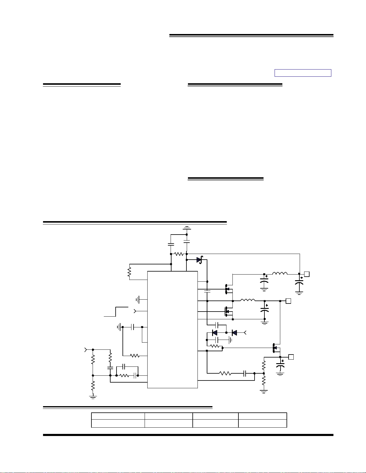
TYPICAL APPLICATION
Vout1
1uF
10
PVCC
BST
Hdrv
SW
Ldrv
Pgnd
NX2201
LDO_Drv
LDO_FB
MBR0530T1
1n4148
0.1u
0.1u
1u
10k
10k 10nF
IRF7822
1.5uH
IRF7822
1n4148
10k
4.7K
OFF
1k
2.7nF
10k
ON
62pF
18k
1uF
VCC
Pgood
GND (PAD)
EN
100p
100p
20k
1.5nF
Vref
Vp
Rt
COMP
FB
Figure1 - Typical application of 2201
ORDERING INFORMATION
Device Temperature Package Pb-Free
NX2201CMTR 0 to 70oC MLPQ-16L Yes
5V
1uH
6.3V,390uF
POSCAP
2*(220uF,12mohm)
MTD3055
100
100
6.3V/100uF
Vout1
Vout2
5V VIN
33uF
2.5V@9A
1.6V@2A
Rev. 1.0
01/24/05
www.nexsem.com
1
Page 2
NEXSEM
θ≈46/
CW
ABSOLUTE MAXIMUM RATINGS(NOTE1)
Vcc to GND & BST to SW voltage ................... 6.5V
BST to GND Voltage ...................................... 35V
Storage Temperature Range ............................. -65oC to 150oC
Operating Junction Temperature Range ............. -40oC to 125oC
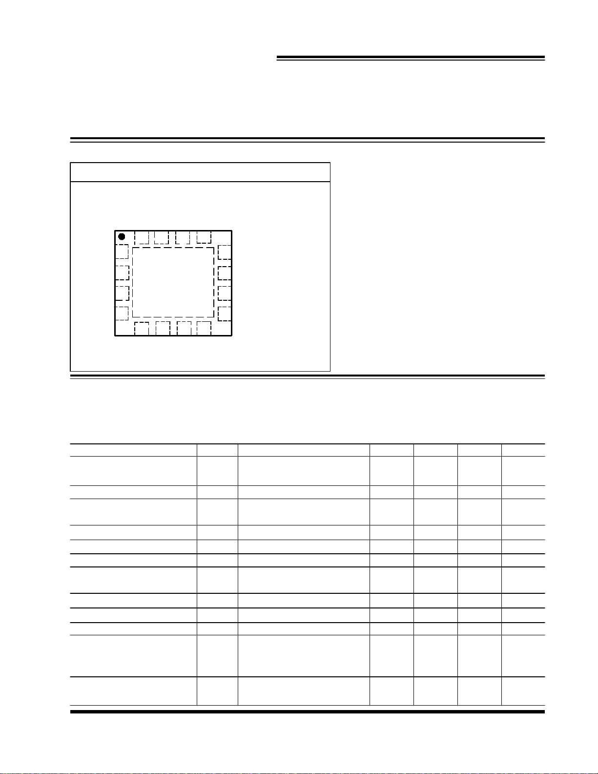
PACKAGE INFORMATION
16-LEAD PLASTIC MLPQ
NX2201
SW
17
AGND
6
RT
LDO_OUT
LDO_FB
87
EN
VREF
12
11
10
9
PGOOD
COMP
FB
VP
o
JA
BST
PGND
LDRV
PVCC
HDRV
16 15 14 13
1
2
3
4
5
VCC
ELECTRICAL SPECIFICATIONS
Unless otherwise specified, these specifications apply over Vcc = 5V, and TA= 0 to 70oC. Typical values refer to Ta
= 25oC. Low duty cycle pulse testing is used which keeps junction and case temperatures equal to the ambient
temperature.
PARAMETER SYM TEST CONDITION MIN TYP MAX UNITS
Feedback Voltage
FB Voltage
FB Voltage Line Regulation
Vcc supply voltage
UVLO Threshold - Vcc
UVLO Hysteresis - Vcc
UVLO Threshold - BST
UVLO Threshold - FB
Supply Current
Vcc Dynamic Supply Current
BST Dynamic Supply Current
Vcc Static Supply Current
BST Static Supply Current
Soft Start Section
Soft start time
Error Amp
Transconductance g
V
VCC_
I
I
I
V
V
CC_DYN
BST_DYN
I
CC_STA
BST_STA
4.5 < Vcc < 5.5
REF
Supply Ramping Up
CC
Hyst
Supply Ramping Up
BST
FB Ramping Down
Freq =300KHz, Cl = 3300pF
Freq = 300KHz, Cl = 3300pF
Fsw=300Khz, 2211
T
ss
Fsw=1Mhz, 2210
m
0.800
0.2
4.1
0.22
2.4
0.4
5
5
3
0.1
3.4
1.02
2500
V
%
V
V
V
V
mA
mA
mA
mA
mS
mS
umho
Rev. 1.0
01/24/05
www.nexsem.com
2
Page 3
NEXSEM
NX2201
PARAMETER SYM TEST CONDITION MIN TYP MAX UNITS
Oscillator
Frequency F
Ramp Amplitude V
Output Drivers
HDRV source impedance
HDRV sink impedance
LDRV source impedance
LDRV sink impedance
Rise Time T
Fall Time T
Dead Band Time T
Max Duty Cycle D
Min Duty Cycle D
EN
Enable Threshold Voltage
Enable Hysterises
Power Good
Threshold
Hysteresis
PGood Voltage Low
LDO Controller
LDO FB voltage
LDO FB Bias Current
LDO OUT drive Vsat voltage
RISE
S
RAMP
FALL
dead
max
min
NX2211
NX2210
I=200mA
I=200mA
I=200mA
I=200mA
Cload = 1500pF
Cload = 1500pF
LDRV Low to HDRV High
FB = 0.6V
FB = 1V
Enable ramp up
LDO OUT=LDO FB
-0.2
I=10mA
600
1000
2
0.9
0.65
0.9
0.5
50
50
30
95
1.6
0.1
0.9V
0.05V
0.2
0.8
0
0.4
KHz
KHz
Vpp
ohm
ohm
ohm
ohm
0
REF
REF
0.2
nS
nS
nS
%
%
V
V
V
V
V
V
uA
V
NOTE1: Stresses above those listed in "ABSOLUTE MAXIMUM RATINGS", may cause permanent damage to
the device. This is a stress only rating and operation of the device at these or any other conditions above those
indicated in the operational sections of this specification is not implied.
Rev. 1.0
01/24/05
www.nexsem.com
3
Page 4
NEXSEM
PIN DESCRIPTIONS
PIN # PIN SYMBOL PIN DESCRIPTION
1 BST
This pin supplies voltage to the high side driver. A high frequency
ceramic capacitor of 0.1 to 1 uF must be connected from this pin to SW pin.
NX2201
16 HDRV
2 PGnd
3 LDRV
5 Vcc
6 Rt
7 EN
10 FB
11 COMP
High side MOSFET gate driver.
Power ground pin. This pin must be connected directly using a via to ground plane.
Low side MOSFET gate driver.
Voltage supply for the internal circuit. A 1uF high frequency ceramic capacitor must
be connected from this pin to ground plane using a via. A resistor of 10ohm can be
placed from this pin to PVcc pin to form a low pass filter for further noise reduction.
Add resistor to this pin for adjustable frequency which is from 2kHz to 1MHz
Pull up this pin to Vcc for normal operation. Pulling this pin down below 1.25V
shuts down the controller and resets the soft start. This pin can also be used as a
UVLO detector for the bus voltage via a resistor divider.
FB pin is the error amplifier inverting input. This pin is also connected to the output
UVLO comparator. When this pin falls below 0.4V, both HDRV and LDRV outputs
are latched off.
This pin is the output of the error amplifier and together with FB pin is used to
compensate the voltage control feedback loop. This pin is also used as a shut down
pin.
15 SW
12 PGood
13 LDO_FB
14 LDO OUT
8 Vref
9 Vp
4 Pvcc
PAD AGnd
Rev. 1.0
01/24/05
This pin is connected to the source of the high side MOSFET and provides return
path for the high side driver.
This is an open drain output and it is pulled low if the FB voltage is below 90% of the
Vref. If not used it may be left floating.
LDO controller feedback input.
LDO controller output. This pin is an open drain output controlling the gate of an
external NCH MOSFET thru a pull up resistor to a voltage higher than the drain by at
least 5V. The maximum rating of this pin is 16V.
Output of the internal reference voltage. A capacitor of 100pF to 1000pF may be
placed from this pin to Gnd to reduce high frequency noise.
This pin is the error amplifier noninverting input. It should be connected to the Vref
pin.
Voltage supply for the low side MOSFET gate driver. A 1uF high frequency ceramic
capacitor must be connected from this pin to ground plane using a via.
Analog ground pin. This pin must be connected directly using via to ground plane.
www.nexsem.com
4
 Loading...