

Page 1
NX2155H
SINGLE POWER SUPPLY SYNCHRONOUS PWM CONTROLLER
ADVANCED DATA SHEET
Pb Free Product
DESCRIPTION
The NX2155H controller IC is a single input supply synchronous Buck controller IC designed for step down DC
to DC converter applications. NX2155H is optimized to
convert bus voltages from 8V to 22V to output as low as
0.8V voltage. An internal regulator converts bus voltage
to 5V, which provides voltage supply to internal logic
and driver circuit. The NX2155H can operates at programmable frequency of 2MHz and employs loss-less
current limiting by sensing the Rdson of synchronous
MOSFET followed by hiccup feature.Feedback under
voltage triggers Hiccup.
Other features of the device are: Internal schottky diode, thermal shutdown, 5V gate drive, adaptive
deadband control, internal digital soft start, 5VREG
undervoltage lock out and Shutdown capability via the
comp pin.
0.1u
4.7u
4.22k
6
VIN
5
5VREG
7
RT
8
COMP
N X 2 1 5 5 H
GND(PAD)
BST
HDRV
SW
OCP
LDRV
FB
3
2
1
10
4
9
0.1u
6k
1n
FEATURES
n Single supply voltage from 8V to 22V
n Internal 5V regulator
n Programmable operational frequency of 2MHz
n Internal Digital Soft Start Function
n Less than 50 nS adaptive deadband
n Current limit triggers hiccup by sensing Rdson of
Synchronous MOSFET
n Pb-free and RoHS compliant
APPLICATIONS
n LCD TV
n Graphic Card on board converters
n Memory Vddq Supply in mother board applications
n On board DC to DC such as
12V to 3.3V, 2.5V or 1.8V
n Hard Disk Drive
n Set Top Box
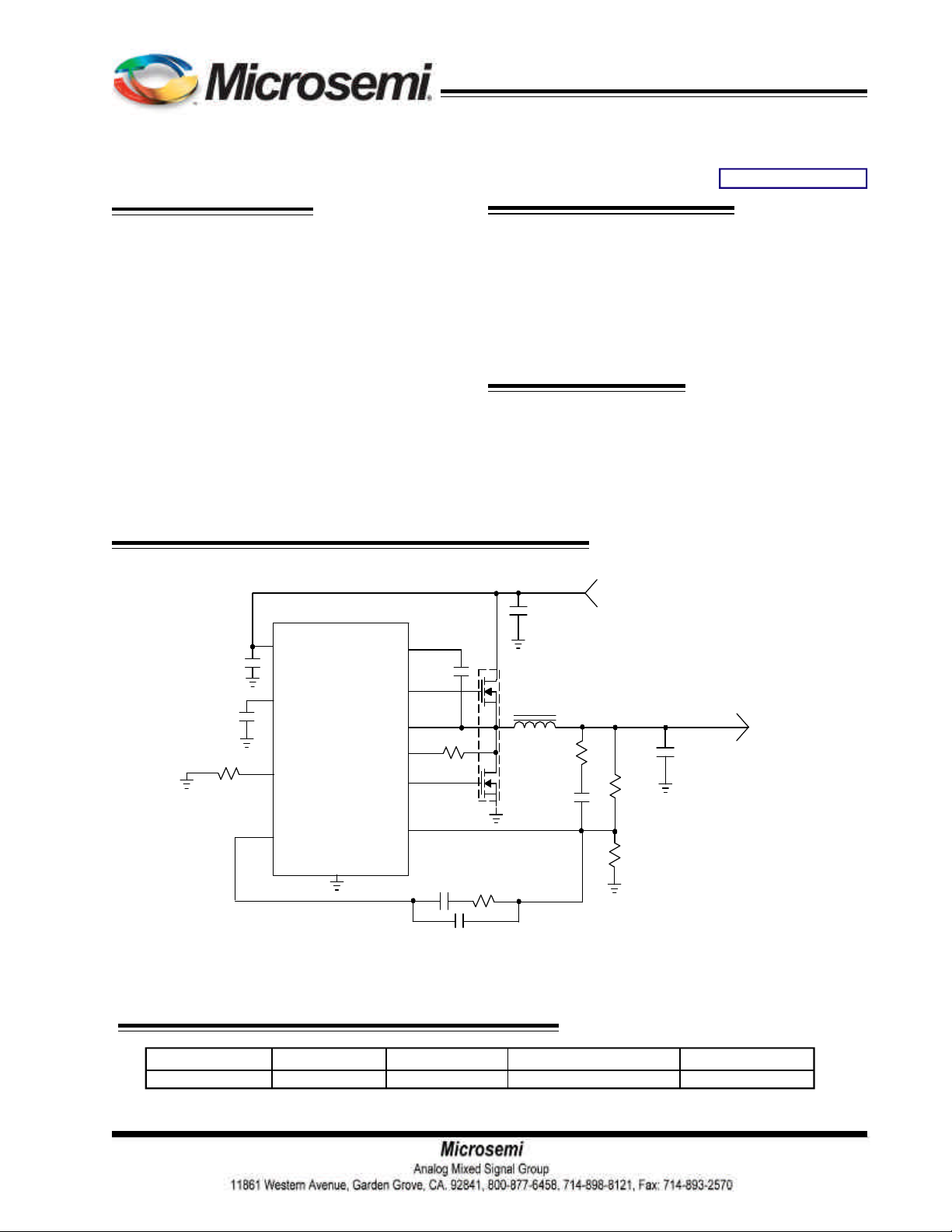
TYPICAL APPLICATION
VIN
300
+12V
VOUT
+5V@2A
2 x (10uF,10V,X5R)
49.9k
9.53k
10u
M1
AO6800
1u
180p
15k
10p
Figure1 - Typical application of 2155H
ORDERING INFORMATION
Device Temperature Package Package Marking Pb-Free
NX2155HCUPTR 0 to 70oC MSOP-EP-10L NX155HXXX Yes
Note: XXX is date code. For example, 841 means that this NX2155H is packaged in the 41th week of
2008
Rev.1.1
04/16/09
1
Page 2
NX2155H
CW
θ≈46/
Supply Voltage(Vin)
ABSOLUTE MAXIMUM RATINGS(NOTE1)
VCC to GND & BST to SW voltage ................... 6.5V
BST to GND Voltage ...................................... 30V
VIN to GND Voltage ........................................ 25V
SW to GND .................................................... -2V to 35V
All other pins .................................................. -0.3V to 6.5V
Storage Temperature Range ............................. -65oC to 150oC
Operating Junction Temperature Range ............. -40oC to 125oC
NOTE1: Stresses above those listed in "ABSOLUTE MAXIMUM RATINGS", may cause permanent damage to
the device. This is a stress only rating and operation of the device at these or any other conditions above those
indicated in the operational sections of this specification is not implied.
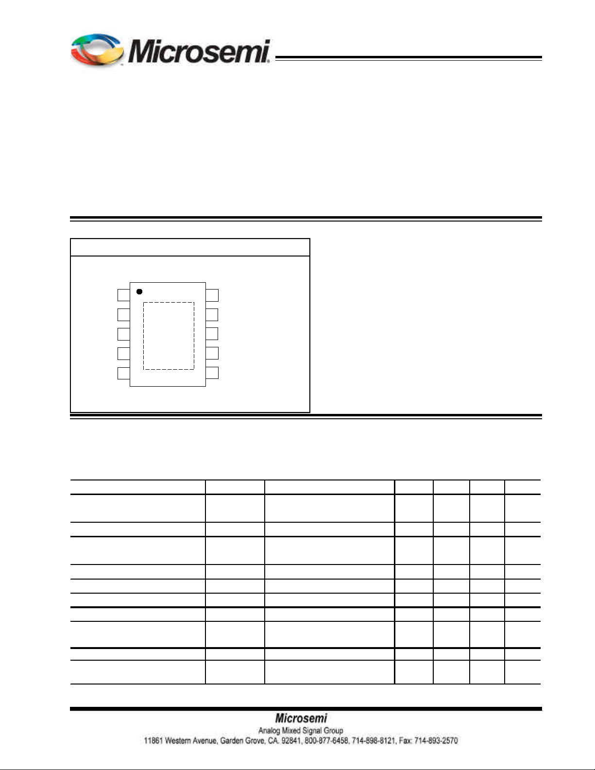
PACKAGE INFORMATION
10-LEAD PLASTIC MSOP-EP
o
SW
HDRV
BST
LDRV
5VREG
JA
1
2
3
4
5
GND
(PAD)
10
9
8
7
6
OCP
FB
COMP
RT
VIN
ELECTRICAL SPECIFICATIONS
Unless otherwise specified, these specifications apply over Vin = 12V, and TA = 0 to 70oC. Followings are bypass
capacitors:C
pulse testing is used which keeps junction and case temperatures equal to the ambient temperature.
Reference Voltage
Ref Voltage V
Ref Voltage line regulation Vin=8V to 22V 0.4 %
5VREG
5VREG Voltage range
5VREG UVLO 5V REG rising
5VREG UVLO Hysteresis
5VREG Line Regulation VIN=9V to 22V 10
5VREG Max Current
=1uF, C
VIN
PARAMETER SYM Test Condition Min TYP MAX Units
=4.7uF, all X5R ceramic capacitors. Typical values refer to TA = 25oC. Low duty cycle
5VREG
REF
0.784
4.75
20
0.8
3.9
0.2
0.816
5
5.25
4.4
20
50 mA
V
V
V
V
mV
Vin Voltage Range V
Input Voltage Current(Static) No switching 3.7 4.8 6.5 mA
Input Voltage Current
(Dynamic)
Rev.1.1
04/16/09
in
Switching with HDRV and
LDRV open @2.2MHz
8 22
5.4 8 11 mA
V
2
Page 3
NX2155H
FBUVLO
Feedback UVLO threshold
0.54
0.6
0.66
V
sink
Rise Time
TLdrv(Rise)
13 ns
OCP
Over temperature
C
C
Internal Schottky Diode
PARAMETER SYM Test Condition Min TYP MAX Units
Vin UVLO
Vin-Threshold Vin_UVLO Vin Rising
6
Vin-Hysteresis Vin_Hyst Vin Falling 0.6 V
SS
Soft Start time Tss FS=2.2MHz 400 uS
Oscillator (Rt)
Frequency F
Ramp-Amplitude Voltage V
S
RAMP
Max Duty Cycle FS=2.2MHz
Rt=4.22k
1.4
62
Min Controlable On Time
Error Amplifiers
Transconductance 1500 2000 2500 umho
Input Bias Current Ib 10 nA
Comp SD Threshold 0.24 0.3 0.36 V
High Side Driver(CL=2200pF)
Output Impedance , Sourcing R
Output Impedance , Sinking R
(Hdrv) I=200mA 1.9 ohm
source
(Hdrv) I=200mA 1.7 ohm
sink
Rise Time THdrv(Rise) 14 ns
Fall Time THdrv(Fall) 17 ns
Deadband Time Tdead(L to H)Ldrv going Low to Hdrv
21 30 39 ns
going High, 10%-10%
Low Side Driver (CL=2200pF)
Output Impedance, Sourcing
R
(Ldrv) I=200mA 1.9 ohm
source
Current
Output Impedance, Sinking R
(Ldrv) I=200mA 1 ohm
6.5
2250
1.5
71
7.5
1.9
80
150
V
kHz
V
%
nS
Fall Time TLdrv(Fall) 12 ns
7
10 13 nsDeadband Time Tdead(H to L)SW going Low to Ldrv
going High, 10% to 10%
OCP current 30 37 45 uA
Threshold
150
Hysteresis 20
o
o
Forward voltage drop forward current=20mA 350 500 mV
Rev.1.1
04/16/09
3
Page 4
PIN DESCRIPTIONS
PIN # PIN SYMBOL PIN DESCRIPTION
5 5VREG
An internal 5V regulator provides supply voltage for the low side fet driver, BST
and internal logic circuit. A high frequency 4.7uF X5R ceramic capacitor must
be connected from this pin to the GND pin as close as possible.
NX2155H
6 VIN
9 FB
8 COMP
3 BST
10 OCP
1 SW
2 HDRV
Voltage supply for the internal 5V regulator. A high freuqncy 0.1uF ceramic capacitor must be connected from this pin to GND.
This pin is the error amplifier inverting input. This pin is also connected to the
output UVLO comparator. When this pin falls below threshold, both HDRV and
LDRV outputs are in hiccup.
This pin is the output of the error amplifier and together with FB pin is used to
compensate the voltage control feedback loop. This pin is also used as a shut
down pin. When this pin is pulled below 0.3V, both drivers are turned off and
internal soft start is reset.
This pin supplies voltage to the high side driver. A high frequency
ceramic capacitor of 0.1 to 1 uF must be connected from this pin to SW pin.
This pin is connected to the drain of the external low side MOSFET and is the
input of the over current protection(OCP) comparator. An internal current source
is flown to the external resistor which sets the OCP voltage across the Rdson
of the low side MOSFET. Current limit point is this voltage divided by the Rdson.
This pin is connected to the source of the high side MOSFET and provides return
path for the high side driver.
High side MOSFET gate driver.
PAD GND
4 LDRV
7 RT
Rev.1.1
04/16/09
Ground pin.
Low side MOSFET gate driver.
Oscillator's frequency can be set by using an external resistor from this pin to
GND.
4
Page 5
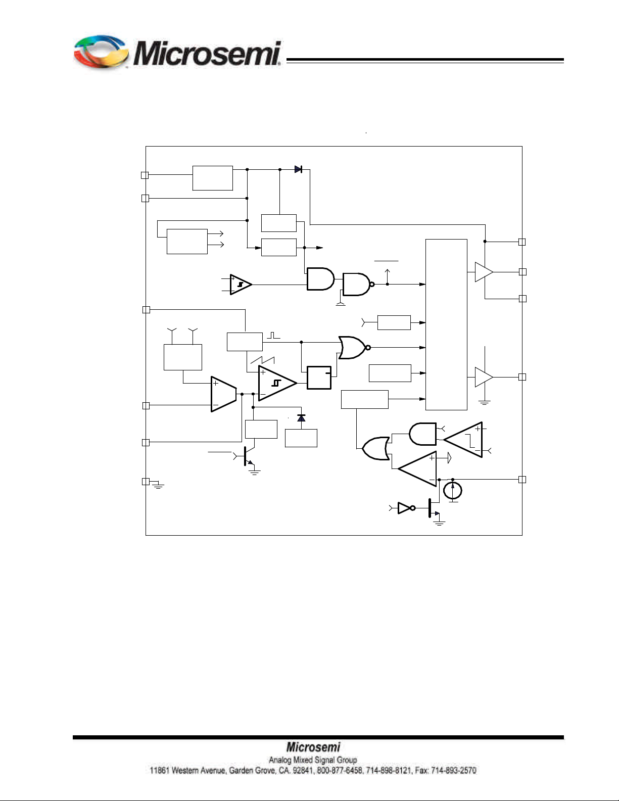
BLOCK DIAGRAM
NX2155H
VIN
5VREG
RT
FB
COMP
Bias
Generator
START
Digital
start Up
5V
Regulator
0.8V
COMP
0.3V
START
1.25V
0.8V
ramp
OSC
0.6V
CLAMP
UVLO
UVLO
1.3V
CLAMP
POR
START
OC
OVP
S
Q
R
Hiccup Logic
Latch
PWM
Thermal
Shutdown
Control
Logic
SS_done
VCC
0.6V
FB
BST
HDRV
SW
LDRV
Rev.1.1
04/16/09
GND
START
Figure 2 - Simplified block diagram of the NX2155H
OCP
VCC
5
Page 6
NX2155H
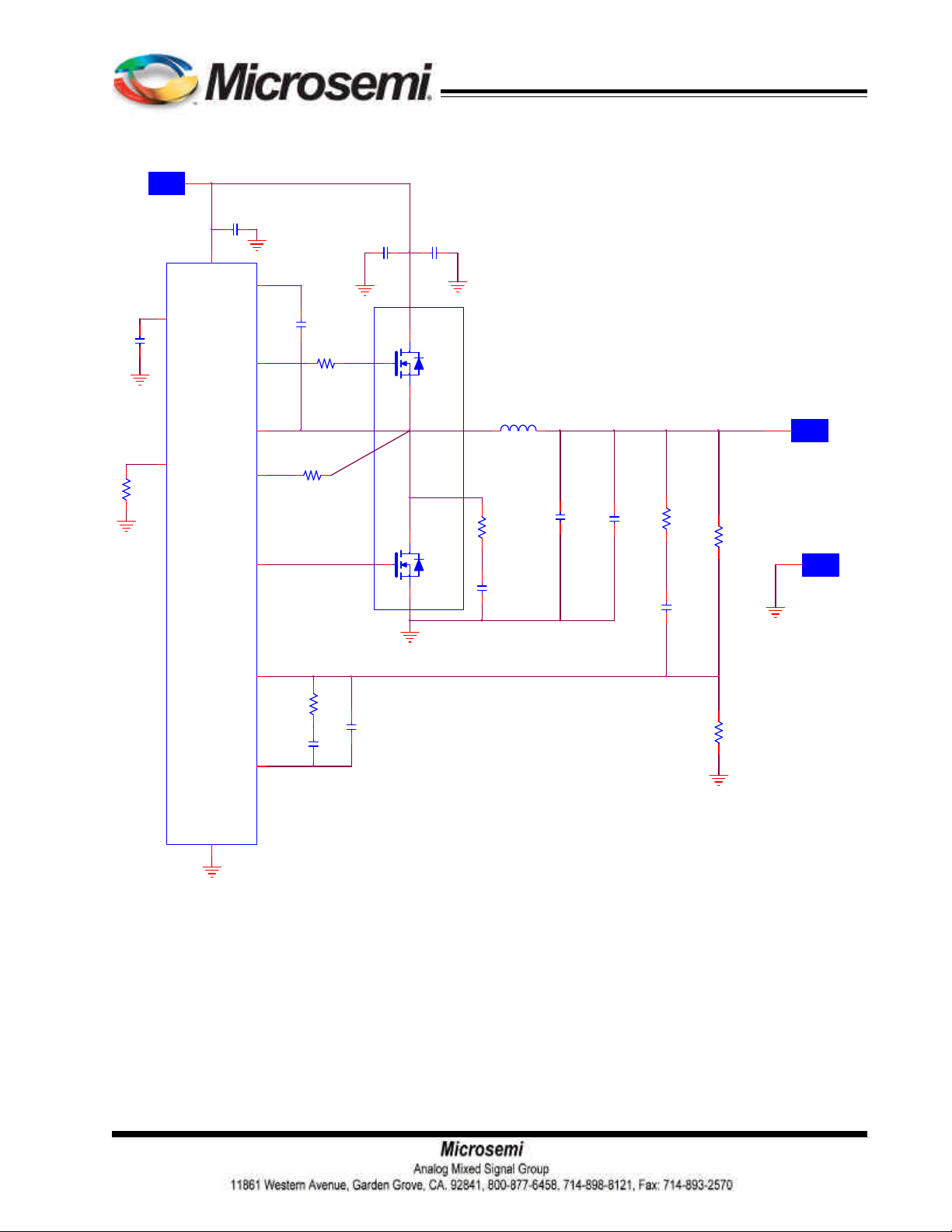
Demoboard Design(VIN=12V, VOUT= 5V/2A, FREUQNCY=2.2MHz)
sdfd
BUS
C1
C2
4.7u
R1
4.22k
10uF,16V
HDRV
CIN2
3
0.1u
6
3
VIN
BST
5
VCC
HDRV
C3
0.1u
2
R8
0
U1
1
SW
7
RT
OCP
LDRV
R2
10
6k
LDRV
4
1
0.1uF
4
M1B
AO6800
2
6
M1A
AO6800
5
CIN1
SW
BRL3225T1R0M
R7
10
C7
470p
L1
COUT1
10uF,16V
GND
OUT
COUT2
10uF,16V
R3
300
C4
180p
VOUT
R4
49.9k
GND
9
FB
NX2155H/MSOP-EP10
8
COMP
GNDPAD
11
* R7 and C7 are optional.
R6
15k
C6
10p
C5
1n
Figure 3 - Simplified demoboard schematic of NX2155H
R5
9.53k
Rev.1.1
04/16/09
6
Page 7
NX2155H
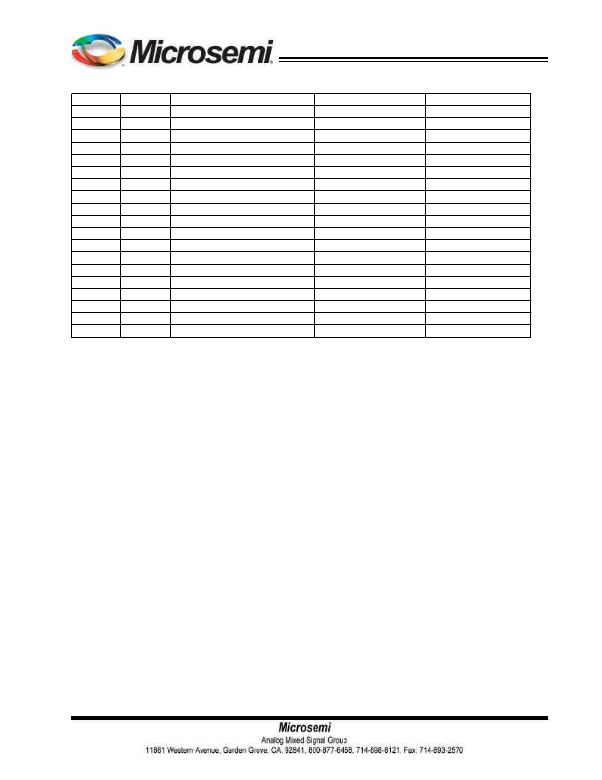
Bill of Materials
Item Quantity Reference Part Manufacturer
1 3 C1,C3,CIN1 0.1u
2 1 C2 4.7uF,6.3V,X5R
3 1 C4 180p
4 1 C5 1n
5 1 C6 10p
6 1 C7 470p
7 1 CIN2 10uF,16V,X5R
8 2 COUT1,COUT2 10uF,10V,X5R
9 1 L1 BRL3225T1R0M TAIYO YUDEN
10 1 M1 AO6800 AOS
11 1 R1 4.22k
12 1 R2 6k
13 1 R3 300
14 1 R4 49.9k
15 1 R5 9.53k
16 1 R6 15k
17 1 R7 10
18 1 R8 0
19 1 U1 NX2155H/MSOP-EP10 NEXSEM INC.
Rev.1.1
04/16/09
7
Page 8
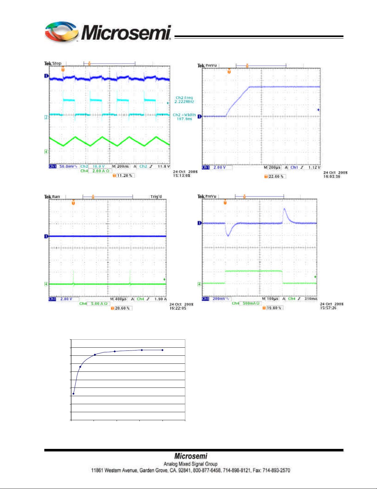
Demoboard Waveforms
Efficiency (%)
NX2155H
Fig.4 Output ripple(CH1 VOUT AC 50mV/DIV, CH2
SW 10V/DIV, CH4 OUTPUT CURRENT 2A/DIV)
Fig.6 OCP protection during output short(CH1 VOUT
2V/DIV, CH4 OUTPUT CURRENT 5A/DIV)
100.00%
90.00%
80.00%
70.00%
60.00%
50.00%
40.00%
30.00%
20.00%
10.00%
0.00%
0 500 1000 1500 2000 2500
Iout (mA)
Fig.8 Output efficiency
Fig.5 Startup( CH1 VOUT 2V/DIV)
Fig.7 Output dynamic response(CH1 VOUT AC
200mV/DIV, CH4 OUTPUT CURRENT 500mA/DIV)
Rev.1.1
04/16/09
8
Page 9
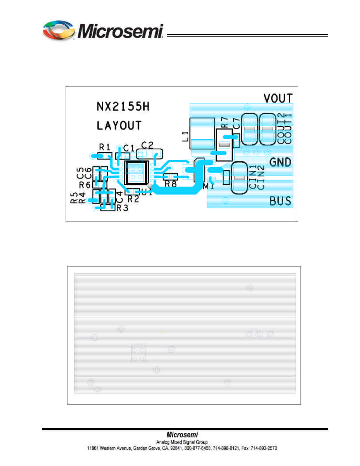
Demoboard Layout
NX2155H
Figure 9 Top layer
Rev.1.1
04/16/09
Figure 10 Ground layer
9
Page 10
NX2155H
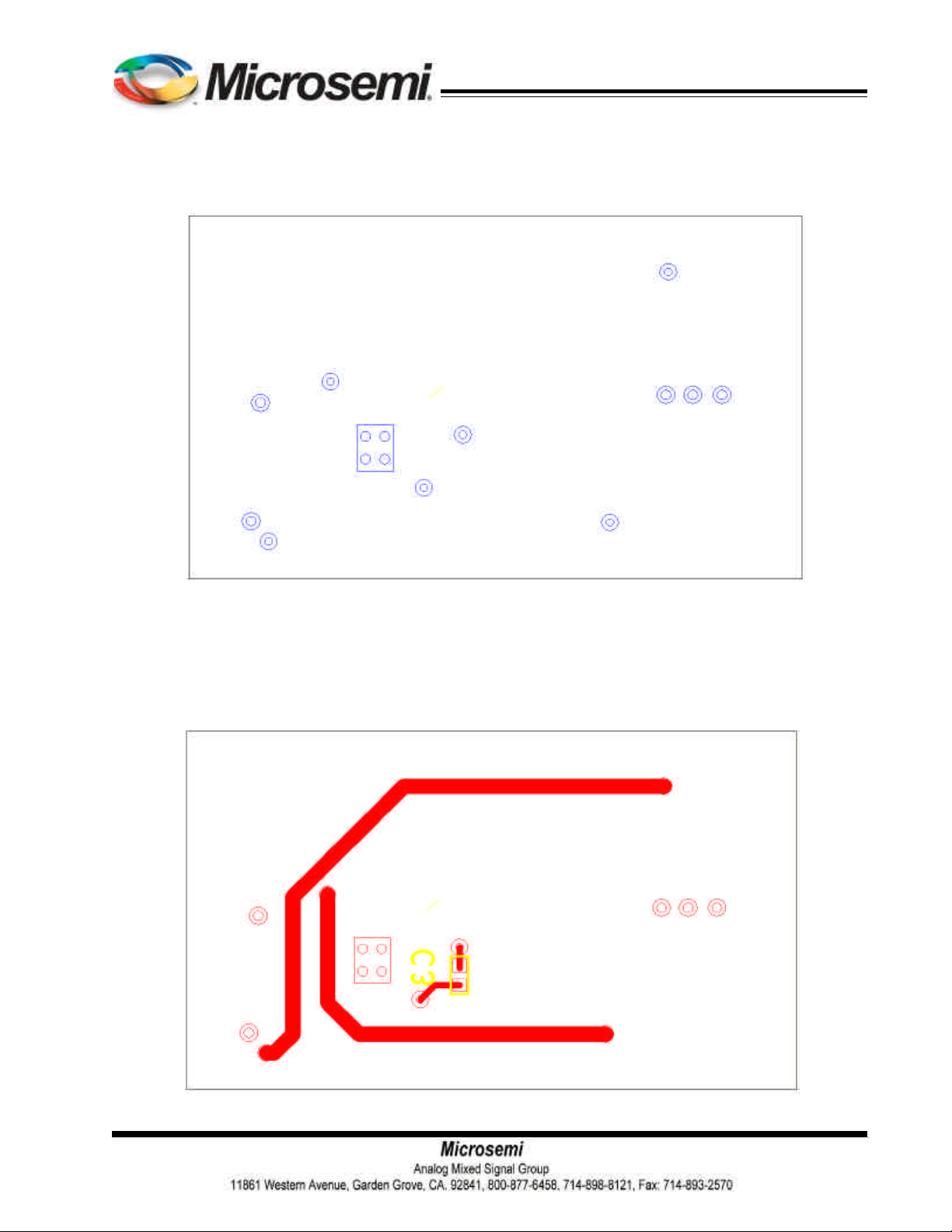
Figure 11 Power layer
Rev.1.1
04/16/09
Figure 12 Bottom layer
10
Page 11
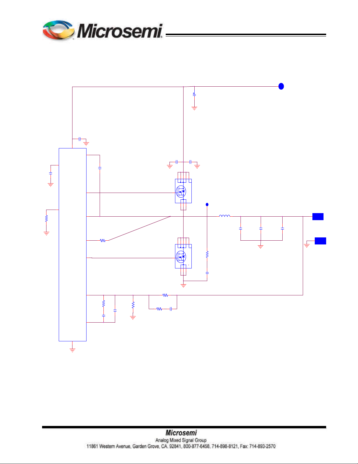
Demoboard Design( (VIN=12V, VOUT= 5V/10A,
FREUQNCY=400kHz)
NX2155H
R3
30k
C5
4.7u
BUS
C18
100u/16v
C3
0.1u
6
3
VIN
BST
5
VCC
U1
HDRV
7
RT
SW
OCP
LDRV
C4
0.1u
2
1
R1
10
3k
4
HDRV
LDRV
NX2155/MSOP-EP10
22u/25V
4
SWSW
4
C9
C10
22u/25V
56789
M1
BSC119N03S
123
56789
M2
123
SW
1 2
DO5010H-222MLD
R17
2.15
BSC029N025S
C13
1000p
L1
C14
47uF/6.3V/X5R
1
C15
47uF/6.3V/X5R
BUS
C19
47uF/6.3V/X5R
VOUT
VOUT
GND
Rev.1.1
04/16/09
FB
COMP
GNDPAD
11
100k
R8
750
R9
C23
220p
9
R7
30k
C22
33p
C21
8
1n
R10
19.1k
Figure 13 - Simplified demoboard schematic of NX2155H
11
Page 12
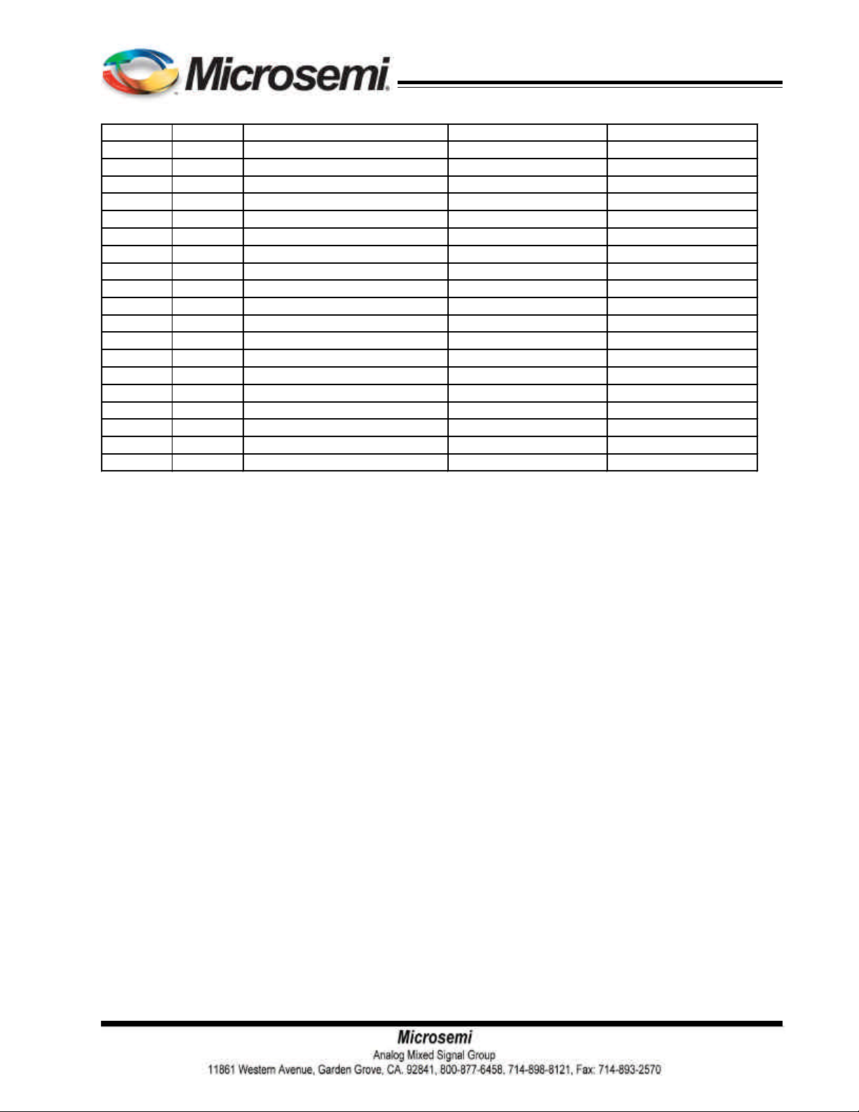
Bill of Materials
Item Quantity Reference Part Manufacturer
1 2 C3,C4 0.1u
2 1 C5 4.7u
3 2 C9,C10 22u/25V/X5R
4 1 C13 1000p
5 3 C14,C15,C19 47uF/6.3V/X5R
6 1 C18 100u/16v
7 1 C21 1n
8 1 C22 33p
9 1 C23 220p
10 1 L1 DO5010H-222MLD COILCRAFT
11 1 M1 BSC119N03S INFINEON
12 1 M2 BSC029N025S INFINEON
13 1 R1 3k
14 2 R3,R7 30k
15 1 R8 750
16 1 R9 100k
17 1 R10 19.1k
18 1 R17 2.15
19 1 U1 NX2155/MSOP-EP10 NEXSEM INC.
NX2155H
Rev.1.1
04/16/09
12
Page 13
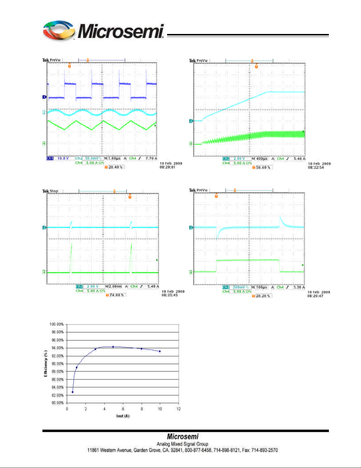
Demoboard Waveforms
NX2155H
Fig.14 Output ripple(CH1 SW 10V/DIV, CH2 VOUT AC
50mV/DIV, CH4 INDUCTOR CURRENT 5A/DIV)
Fig.16 OCP protection during output short(CH2
VOUT 2V/DIV, CH4 OUTPUT CURRENT 5A/DIV)
Fig.15 Startup( CH1 VOUT 2V/DIV, CH4 INDUCTOR
CURRENT 5A/DIV)
Fig.17 Output dynamic response(CH2 VOUT AC
200mV/DIV, CH4 OUTPUT CURRENT 5A/DIV)
Rev.1.1
04/16/09
Fig.18 Output efficiency
13
Page 14
NX2155H
RIPPLEINS
1
IVF
SOUT
F ...(3)
F ...(4)
F ...(5)
F ...(6)
OUT minin1
V1gZZ/R
APPLICATION INFORMATION
Symbol Used In Application Information:
VIN - Input voltage
VOUT - Output voltage
IOUT - Output current
DVRIPPLE - Output voltage ripple
FS - Working frequency
DIRIPPLE - Inductor current ripple
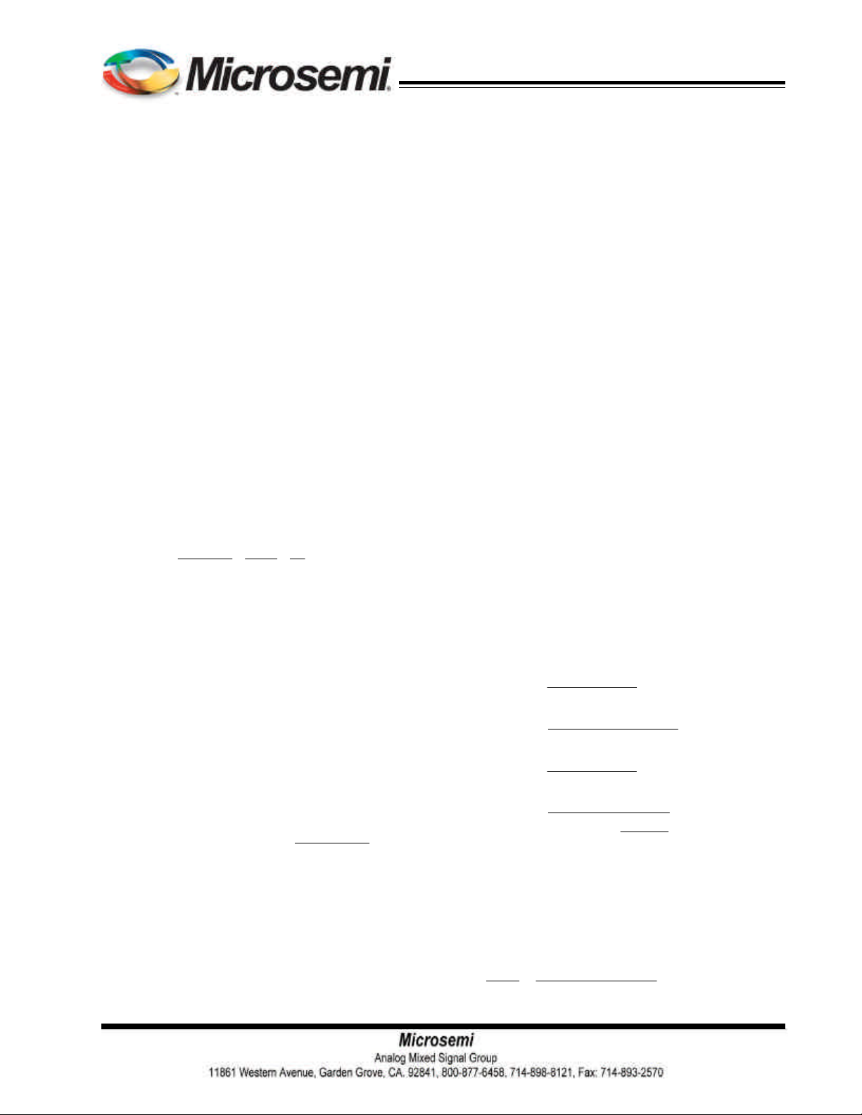
Output Inductor Selection
The selection of inductor value is based on inductor ripple current, power rating, working frequency and
efficiency. Larger inductor value normally means smaller
ripple current. However if the inductance is chosen too
large, it brings slow response and lower efficiency. Usually the ripple current ranges from 20% to 40% of the
output current. This is a design freedom which can be
decided by design engineer according to various application requirements. The inductor value can be calculated by using the following equations:
V-VV
L=
I=kI
where k is between 0.2 to 0.4.
Output Capacitor Selection
Output capacitor is basically decided by the
amount of the output voltage ripple allowed during steady
state(DC) load condition as well as specification for the
load transient. The optimum design may require a couple
of iterations to satisfy both condition.
The amount of voltage ripple during the DC load
condition is determined by equation(2).
∆=×∆+
INOUT OUT
OUT
∆
RIPPLEOUTPUT
VESRI
×
RIPPLERIPPLE
××
...(1)
∆
I
RIPPLE
××
8FC
...(2)
Compensator Design
Due to the double pole generated by LC filter of the
power stage, the power system has 180o phase shift ,
and therefore, is unstable by itself. In order to achieve
accurate output voltage and fast transient response,
compensator is employed to provide highest possible
bandwidth and enough phase margin.Ideally,the Bode
plot of the closed loop system has crossover frequency
between1/10 and 1/5 of the switching frequency, phase
margin greater than 50o and the gain crossing 0dB with 20dB/decade. Power stage output capacitors usually
decide the compensator type. If electrolytic capacitors
are chosen as output capacitors, type II compensator
can be used to compensate the system, because the
zero caused by output capacitor ESR is lower than crossover frequency. Otherwise type III compensator should
be chosen.
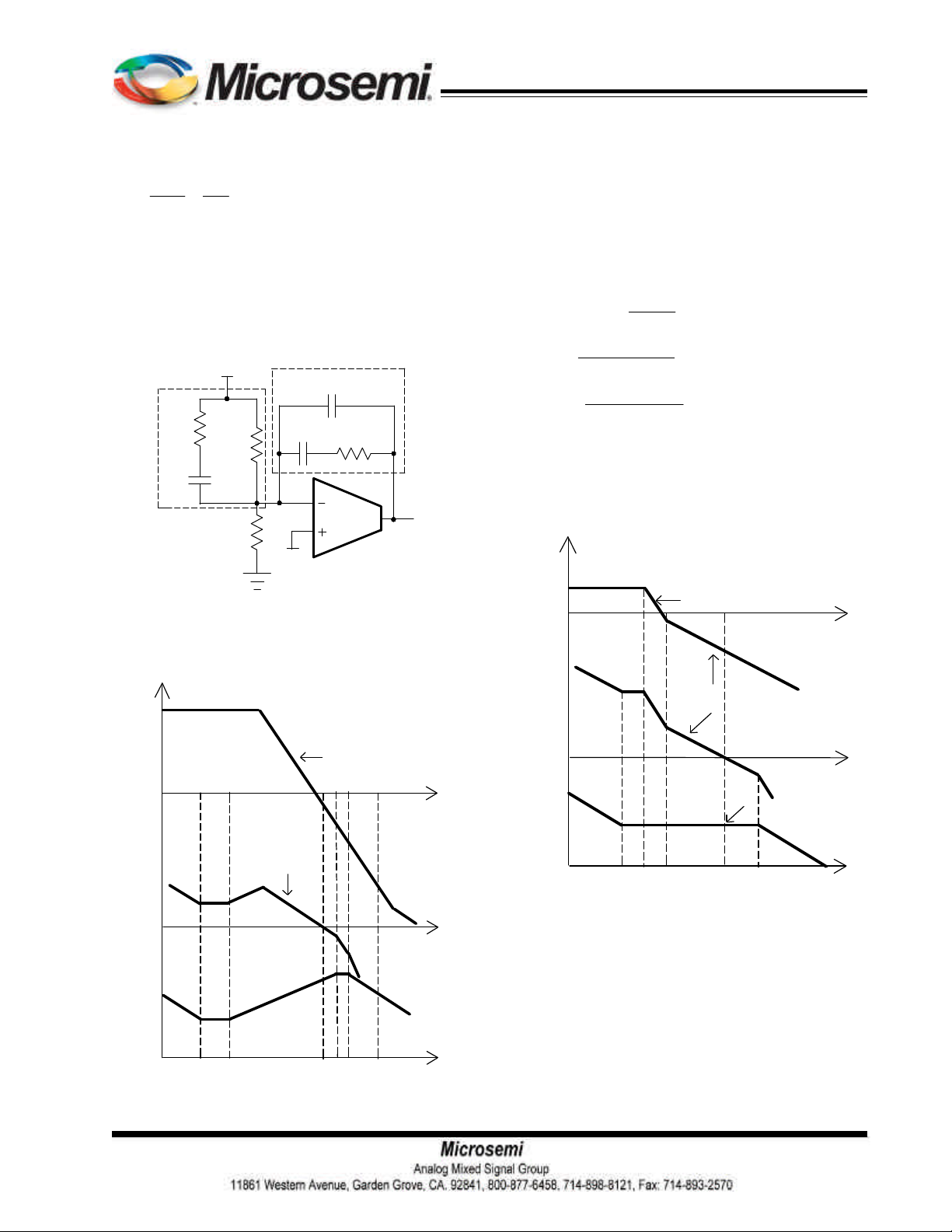
A. Type III compensator design
For low ESR output capacitors, typically such as
Sanyo oscap and poscap, the frequency of ESR zero
caused by output capacitors is higher than the crossover frequency. In this case, it is necessary to compensate the system with type III compensator. The following figures and equations show how to realize the type III
compensator by transconductance amplifier.
1
2RC
×π××
42
1
2(RR)C
×π×+×
233
1
2RC
×π××
33
1
CC
×
2R
×π××
4
CC
12
+
12
=
Z1
=
Z2
=
P1
=
P2
Where ESR is the output capacitors' equivalent
series resistance,C
OUT
Typically when ceramic capacitors are selected as
output capacitors, DC ripple spec is easy to be met, but
mutiple ceramic capacitors are required at the output to
meet transient requirement.
Rev.1.1
04/16/09
is the value of output capacitors.
where FZ1,FZ2,FP1 and FP2 are poles and zeros in
the compensator. Their locations are shown in figure 20.
The transfer function of type III compensator for
transconductance amplifier is given by:
V 1gZ
e mf
=
−×
+×+
14
Page 15
NX2155H
f
OUT in
Z
VZ
−
Gain=gR ... (7)
F= ... (8)
F ... (9)
For the voltage amplifier, the transfer function of
compensator is
V
e
=
To achieve the same effect as voltage amplifier,
the compensator of transconductance amplifier must
satisfy this condition: R
>>2/gm. And it would be desir-
4
able if R1||R2||R3>>1/gm can be met at the same time.
C2
Zf
C1
R4
Zin
Vout
R3
R2
C3
Fb
gm
Ve
R1
Vref
B. Type II compensator design
Type II compensator can be realized by simple RC
circuit without feedback as shown in figure 22. R3 and C
introduce a zero to cancel the double pole effect. C
introduces a pole to suppress the switching noise. The
following equations show the compensator pole zero location and constant gain.
R
1
××
m3
R+R
12
z
≈
p
For this type of compensator, FO has to satisfy
FLC<F
<<FO<=1/10~1/5F
ESR
1
2RC
×π××
31
1
2RC
×π××
32
power stage
s.
1
2
Figure 19 - Type III compensator using
transconductance amplifier
power stage
LC
F
Gain(db)
loop gain
20dB/decade
compensator
40dB/decade
F
O
F
ESR
40dB/decade
Gain(db)
loop gain
20dB/decade
compensator
Gain
F
F
F
LC
Z
ESR
P
F
F
O
Figure 21 - Bode plot of Type II compensator
F
Z1
Figure 20 - Bode plot of Type III compensator
Rev.1.1
04/16/09
F
P1
F
S
F
F
Z2
P2
15
Page 16
Vout
OUT
REF
2REF
OUT REF
SWLDSON
IR+V
OCPOCP
DSON
Frequency(kHz)
R2
Fb
gm
R1
Vref
Ve
R3
C2
C1
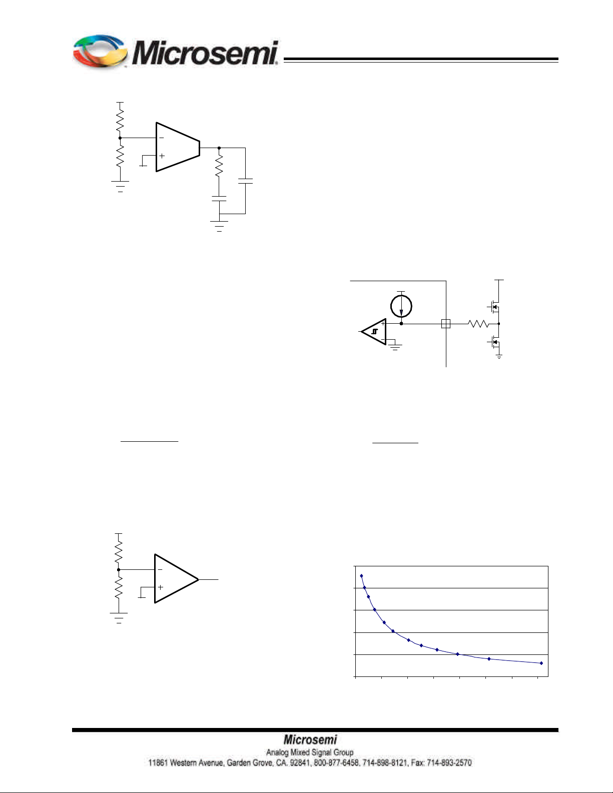
Figure 22 - Type II compensator with
transconductance amplifier
Output Voltage Calculation
Output voltage is set by reference voltage and ex-
ternal voltage divider. The reference voltage is fixed at
0.8V. The divider consists of two ratioed resistors so
that the output voltage applied at the Fb pin is 0.8V when
the output voltage is at the desired value. The following
equation and picture show the relationship between
V ,
V and voltage divider..
NX2155H
Over Current Protection
Over current protection is achieved by sensing current through the low side MOSFET. A typical internal
current source of 37uA flowing through an external resistor connected from OCP pin to SW node sets the over
current protection threshold. When synchronous FET is
on, the voltage at node SW is given as
V=-IR×
The voltage at pin OCP is given as
×
OCPOCPSW
When the voltage is below zero, the over current
occurs.
vbus
OCP
I
OCP
R
OCP
comparator
Figure 24 - Over current protection
The over current limit can be set by the following
equation
SW
OCP
RV
R=
1
×
V-V
...(10)
where R2 is part of the compensator, and the value
of R1 value can be set by voltage divider.
See compensator design for R1 and R2 selection.
Vout
R2
Fb
R1
Vref
Voltage divider
Figure 23 - Voltage divider
SET
×
KR
×
IR
=
I
Frequency Selection
The frequency can be set by external Rt resistor.
The relationship between frequency and RT pin is shown
as follows.
NX2155H Frequency vs Rt
2500
2000
1500
1000
500
0
3 8 13 18 23 28 33 38
Rt(kohm)
Figure 25 - Frequency versus Rt resistor
Rev.1.1
04/16/09
16
Page 17
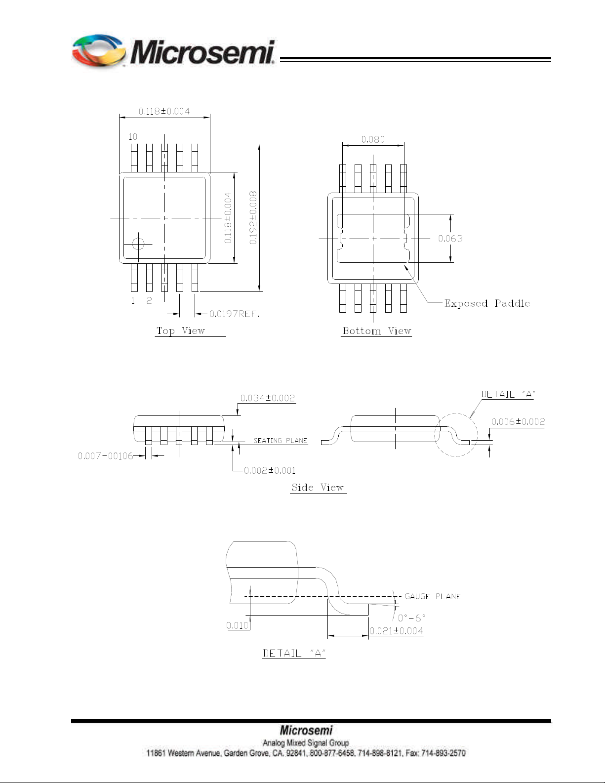
MSOP 10 PIN WITH EXPOSED PAD OUTLINE DIMENSIONS
NX2155H
Rev.1.1
04/16/09
NOTE: ALL DIMENSIONS ARE DISPLAYED IN INCHES.
17
 Loading...