

Page 1
Evaluation board available.
NEXSEM
2A SOURCE/SINK TERMINATION REGULATOR
DESCRIPTION
NX1720 is a 2A source and sink Low Dropout Regulator
designed for DDRI and DDRII termination application.
Current limit circuitry in both sink and source side plus
internal thermal shutdown protects the device under short
circuit condition . NX1720 can be disabled by pulling
down the Reference Pin below 0.2V using external small
signal transistor or a MOSFET.
The NX1720 can also be used as an adjustable output
voltage regulator using an external reference.
NX1720 is available in TO-252 package, standard SOIC8
package as well as SOIC8 with exposed pad package.
NX1720
PRELIMINARY DATA SHEET
Pb Free Product
FEATURES
n Independent Power Sequencing
n Support DDR I (1.25V VTT) and DDRII (0.9V VTT)
n 2A Source and Sink current capability
n Shut down by pulling RefEN pin low
n Current Limit
n Thermal Shut down
n SOIC8, SOICP8 and TO-252 package
n Pb-free and RoHS compliant
APPLICATIONS
n DDR Memory Termination Supply
n Desktop Motherboard or Notebook applications
n Graphic Card
n Set Top Box
n Active Terminal Bus Termination
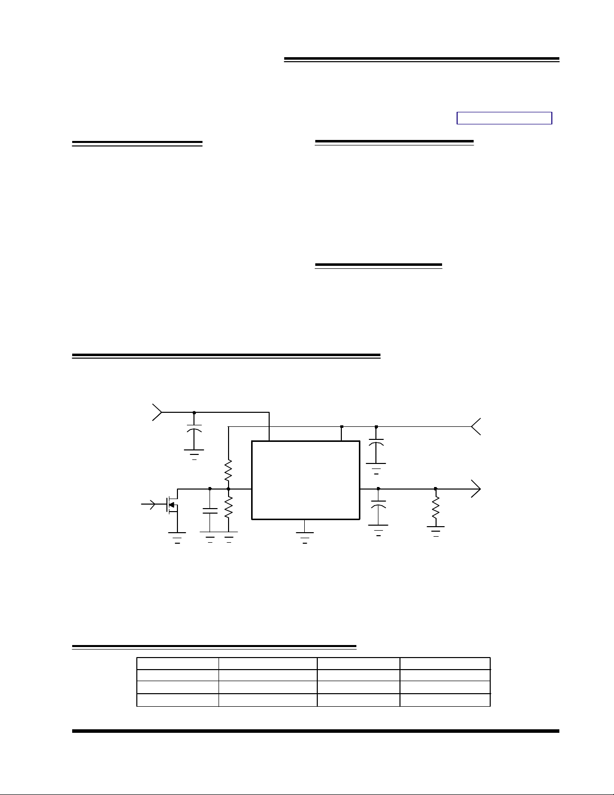
VCNTL
+3.3V
EN
2N7002
C1
0.1uF
CCNTL
1uF
VCNTL
R1
100k
NX1720
REFEN
R2
100k
Figure1 - Typical application of 1720
GND
VIN
VOUT
TYPICAL APPLICATION
VIN
CIN
220uF
Co
220uF
R3
1k
+2.5V
VOUT
+1.25V
Rev. 3.0
03/23/06
ORDERING INFORMATION
Device Temperature Package Pb-Free
NX1720CS1TR 0 to 70oC SOIC - 8L Yes
NX1720CS2TR 0 to 70oC SOICP - 8L Yes
NX1720CDTR 0 to 70oC TO-252 - 5L Yes
www.nexsem.com
1
Page 2
NEXSEM
C/W(NOTE2)
C/W(NOTE3)
C/W
NX1720
ABSOLUTE MAXIMUM RATINGS(NOTE1)
Input Voltage ................................................. 6.5V
Power Dissipation ........................................... Internallly Limited
ESD Susceptibility .......................................... 2kV
Lead Temperature(Soldering,10sec.) ................. 260oC
Storage Temperature Range ............................. -65oC to 150oC
Operating Junction Temperature Range ............. -40oC to 125oC
NOTE1: Stresses above those listed in "ABSOLUTE MAXIMUM RATINGS", may cause permanent damage to
the device. This is a stress only rating and operation of the device at these or any other conditions above those
indicated in the operational sections of this specification is not implied.
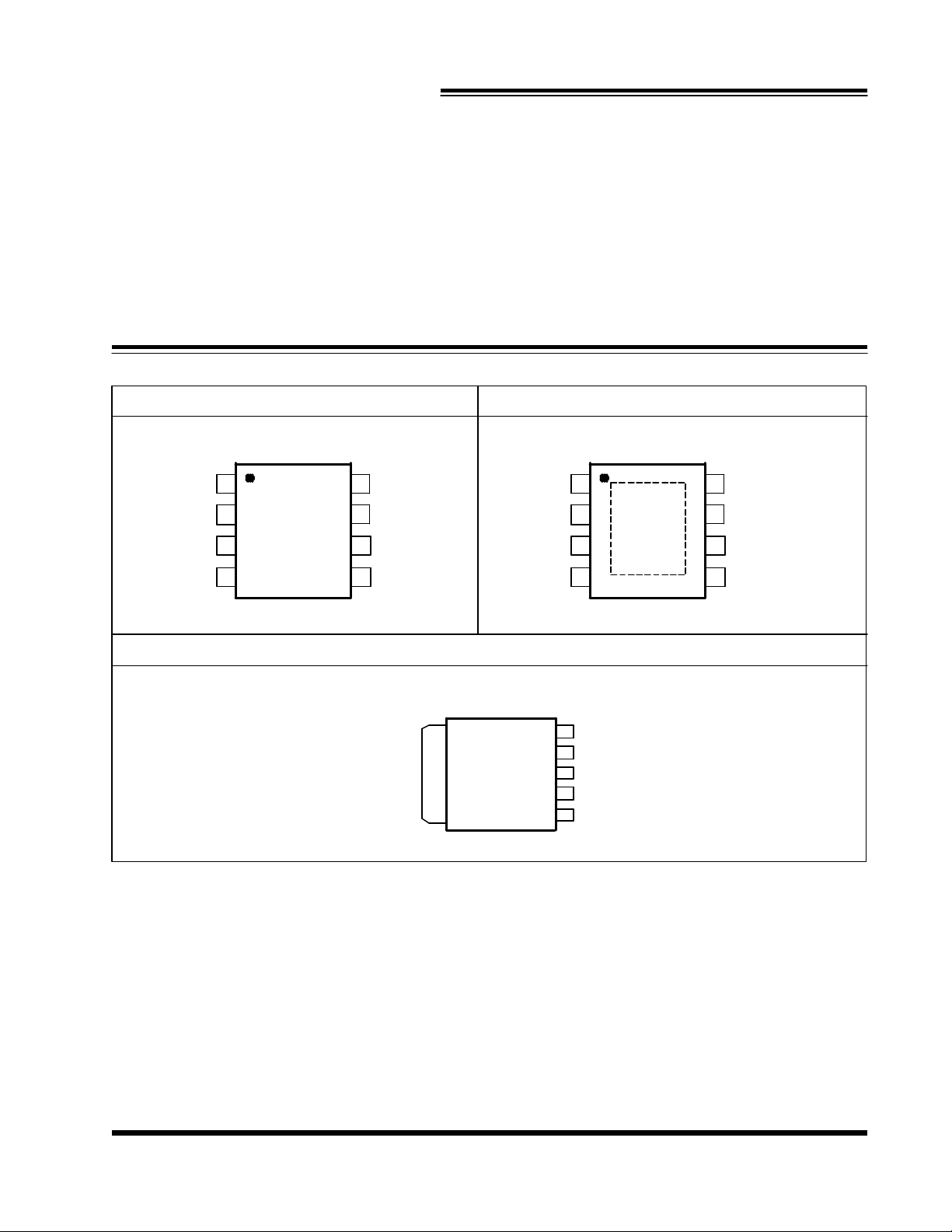
PACKAGE INFORMATION
8-LEAD PLASTIC SOIC 8-LEAD PLASTIC SOICP
VIN
GND
REFEN
VOUT
θ≈96
o
JA
1
2
3
4
NX1720
8
7
6
5
VCNTL
VCNTL
VCNTL
VCNTL
5-LEAD PLASTIC TO_252
θ≈47
o
JA
NX1720
VIN
GND
REFEN
VOUT
1
2
3
4
5
VOUT
4
REFEN
3
VCNTL(TAB)
2
GND
1
VIN
θ≈55
JA
o
NX1720
8
7
6
5
NC
NC
VCNTL
NC
NOTE2: Pin 5-8 internally fused.
NOTE3: Mounted on 1" square copper.
Rev. 3.0
03/23/06
www.nexsem.com
2
Page 3
NEXSEM
Symbol
Pin Description
PARAMETER
SYM
Test Condition
Min
TYP
MAX
Units
OS
Load Regulation
2A
CNTL
SHDNVREFEN
Short Circuit Protection
Protection
Temperature
Shutdown Function
Output=Low
0.2
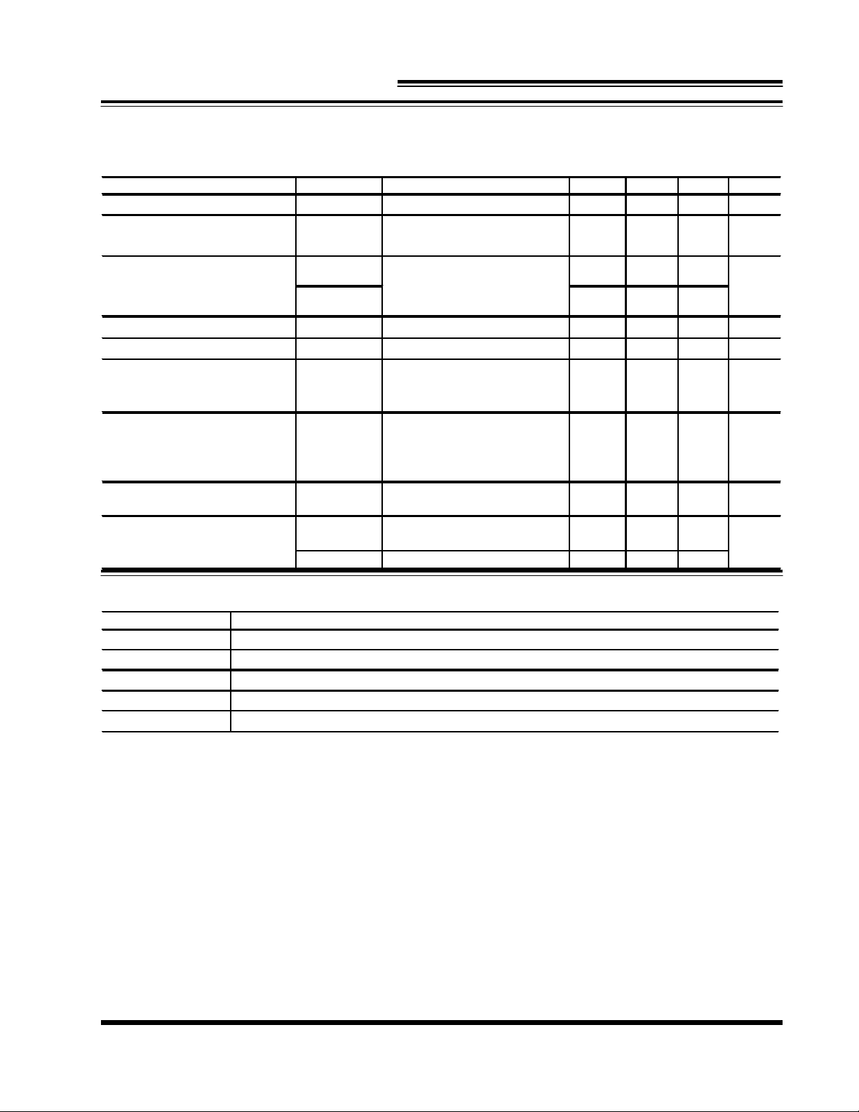
ELECTRICAL SPECIFICATIONS
Unless otherwise specified, these specifications apply over VIN=2.5V, V
C
=220uF(ceramic), and TA = 25oC.
OUT
=3.3V, V
CNTL
NX1720
=1.25V,
REFEN
Output Offset Voltage
Input Voltage Range(DDRI/II)
Operating Current of VCNTL
Current In Shutdown Mode I
Current Limit
Over Temperature
Thermal Shutdown
Thermal Shutdown Hysteresis delta_T
V
delta_V
V
V
CNTL
I
I
LIMIT
T
SD
PIN DESCRIPTIONS
IN
IOUT=0A -20 0 20 mV
IL:From 0A to
LOAD
IL:From 0A to -2A
Keep V
operation power on and
power off sequences
No Load 0.5 mA
<0.2V,RL=180ohm 90 µA
3.3V<=V
SD
Ouput=High 0.6
>=VIN on
CNTL
<=5V 150 °C
CNTL
-20 0 20 mV
1.7 2.5/1.8
3 3.3/5 6
2.1 3.1
35 °C
V
A
VShutdown Threshold Trigger
Rev. 3.0
03/23/06
VIN Regulator's power supply voltage.
GND Ground.
REFEN Reference voltage input.
VOUT Output voltage.
VCNTL Gate drive voltage.
www.nexsem.com
3
 Loading...