

Page 1
PHY/PMD High Speed Copper Media Transceiver
The NWK914D is a Physical Layer device designed for
use in 100BASE-TX applications. The NWK914D has
integrated the 100mb/s transceiver, clock and data recovery
and NRZI conversion circuitry. It is designed for use in cost
effective NIC adapter cards and 100BASE-TX repeater and
switch applications.
The device connects through a 5 bit symbol interface
directly with any MAC controller that includes the PCS layer,
resulting in a simple and cost effective solution. It will also
interface with a PCS device such as the NWK935 to form a
complete 100BASE-TX Physical Layer for connection to the
IEEE 802.3 standard MII interface.
FEATURES
■ Compatible with IEEE-802.3 Standards
■ Operates over 100 Meters of STP and Category 5
UTP cable
■ Five Bit TTL Level Symbol Interface
■ Integrated Clock and Data Recovery
■ Supports Full-duplex Operation
■ Integral 10 Mb/s Buffer for Dual 10 Mb/s & 100 Mb/s
Applications
■ Adaptive Equalization
■ 25MHz to 125MHz Transmit Clock Multiplier
■ Programmable TX Output Current
■ Base Line Wander Correction
Preliminary Information
RDAT4
RDAT3
RDAT2
RDAT1
RDAT0
TXC
48
RXIP
RXIN
49
CC
EQSEL
RXV 1
47
10TXIN
525150
1
TTLGND
2
N/C
3
N/C
4
RXC
5
SDT
RDLV
6
CC
7
N/C
N/C
RXPLLV
RXV
LFRB
LFRA
8
9
10
11
12
CC
13
CC
14151617181920
RXGND
RXPLLGND
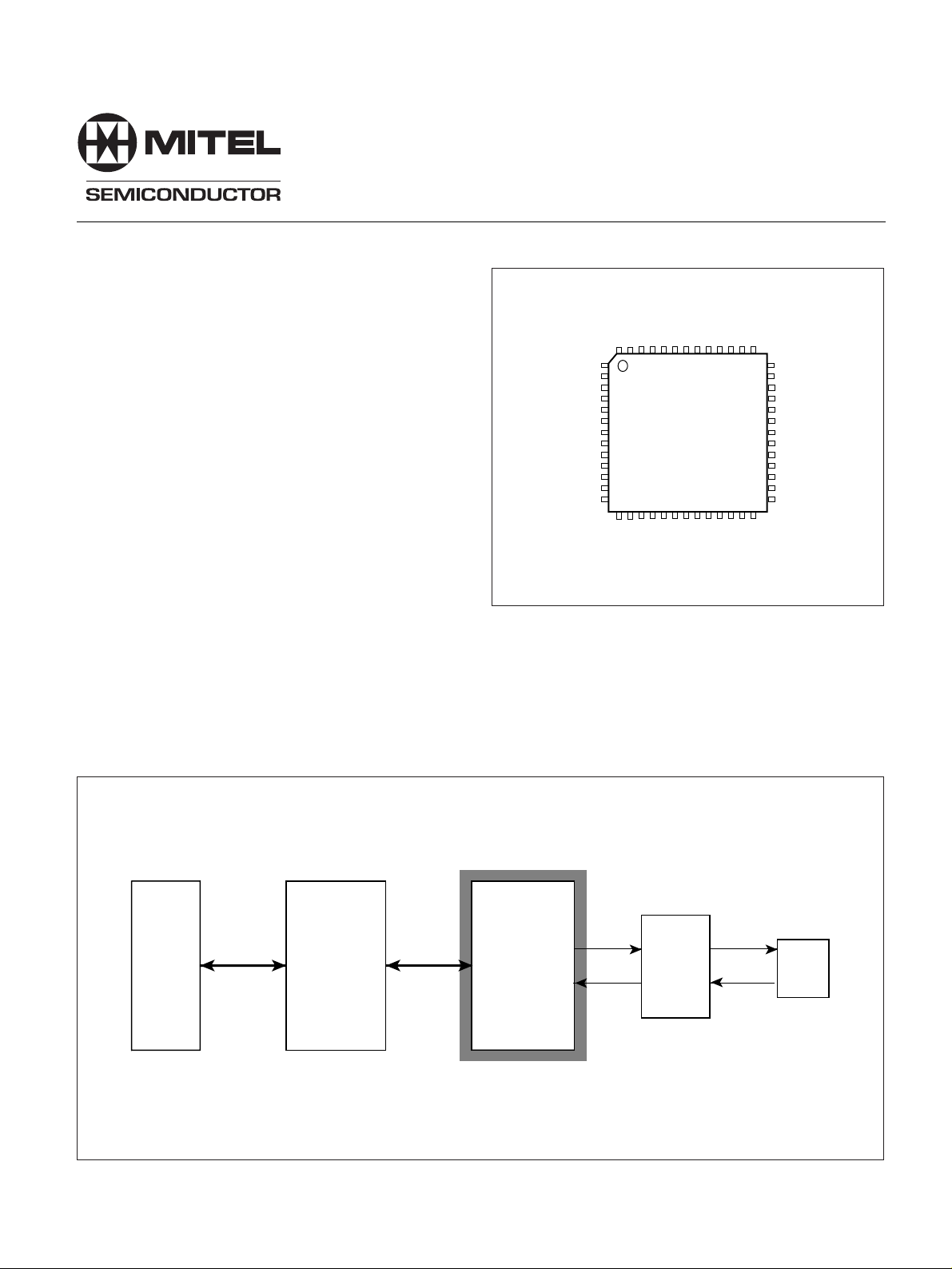
Fig.1 Pin connections - top view
■ Single +5V supply
■ 52 Pin PQFP package
ORDERING INFORMATION
NWK914D/CG/GP1N
NWK914D
NWK914D
DS4829 - 1.1 December 1997
CC
TTLV
REFCLK
TDAT0
TDAT1
TDAT2
TDAT3
22
TXON
23
TXOP
242526
TXREF
TXGND
TDAT4
CC
BGAPV
39
TTLGND
TEST
38
TESTIP
37
N10/100
36
LBEN
35
TDLV
34
33
TXOE
32
TXPLLV
31
LFTA
30
LFTB
29
TXPLLGND
28
BGAPGND
27
SUBGND
CC
CC
GP52
46454443424140
21
CC
TXV
10TXIP
MAC or
Repeater
Controller
IC
MII
Interface
NWK935
100 PCS
Symbol
Interface
NWK914D
Fig.2 Simplified system diagram
Isolation
Magnetics
RJ-45
1
Page 2

NWK914D
ABSOLUTE MAXIMUM RATINGS
Operation at absolute maximum ratings is not implied.
Exposure to stresses outside those listed could cause
permanent damage to the device.
DC Supply voltage (V
) -0.5 to +7V
CC
RECOMMENDED OPERATING CONDITIONS
DC supply voltages (VCC) +5V ±5%
Operating temperature (TA)0°C to +70°C (+25°C typ.)
Power dissipation (P
) 750mW (typ.)
D
Storage temperature (tst) -65 to +150°C
ESD 2kV HBM
ELECTRICAL CHARACTERISTICS
Recommended operating conditions apply except where stated.
Characteristic Symbol Units Conditions
Min. Typ. Max.
DC characteristics
Total V
TTL high level I/P voltage V
supply current I
CC
TTL low level I/P voltage V
TTL high level I/P current I
TTL low level I/P current I
EQSEL high level I/P voltage V
EQSEL low level I/P voltage V
EQSEL floating level I/P V
EQSEL high level I/P current I
EQSEL low level I/P current I
TTL high level O/P voltage V
TTL low level O/P voltage V
TTL high level O/P current I
TTL low level O/P current I
CC
IH
IL
IH
IL
IH
IL
IZ
IH
IL
OH
OL
OH
OL
- 150 - mA device only
2--V
- - 0.8 V
--20µAVIH = V
- - –400 µAVIL = 0.4V
4.2 - - V
- - 0.8 V
-V
- - 1400 µAVIH = V
- - –1400 µAVIL = 0V
2.4 - - V IOH = 20µA
- - 0.5 V IOL = 4mA
- - –200 µA
--4mA
Transmit O/P current - 40 - mA R
pins TXOP, TXON 100Mb/s data
Differential RX I/P - 1.4 - Vp-p measured on device pins
signal voltage 100Mb/s data, 0mCable
RX I/P common mode voltage - V
RX I/P impedance - 24 - kΩ
Signal detect threshold V
TH
- 50 - % wrt normalized output of
Low voltage shutdown - 3.8 - V
Value
/2 - V
CC
= 1300Ω
REF
/2 - V RX I/Ps floating
CC
equalizer
CC
CC
PLL characteristics
3dB bandwidth - 50 - kHz
Damping factor - 2 Peaking - - .005 dB
Overshoot - - 5 %
Static error - ±0.5 - ns
Jitter - - 0.5 ns
VCO characteristics
Centre frequency - 125 - MHz
Deviation - ±40 - MHz
Gain @125MHz - 70 - MHz/V
2
Page 3
NWK914D
REFCLK
TXC
TDAT0
TDAT1
TDAT2
TDAT3
TDAT4
BGAPV
BGAPGND
RXC
RDAT0
RDAT1
RDAT2
RDAT3
RDAT4
10T
LFTB
LFTATTLV
CC
TIMES FIVE
CLOCK
MULTIPLIER
SHIFTER &
NRZ to NRZI
CC
SHIFTER &
NRZI to NRZ
TTLGND1
DIVIDE
CLOCK
by FIVE
TTLGND2 LFRB
125
MHz
RXPLLV
CLOCK
RECOVERY
PLL,125MHZ
LFRA
TXPLLV
CC
LOW VOLTAGE
SHUT DOWN
BAND GAP
VOLTAGE
REFERENCE
CC
SDT
TXOE
TXREF
CURRENT
REFERENCE
NRZI
to
MLT-3
COMPARATORS
MLT-3 to NRZI
TTL
IN 10TXIP
X
SIGNAL
DETECT
ADAPTIVE
EQUALIZER
TXPLLGNDRXPLLGND
TDLV
TESTIP
CC
100
Mb/s
LEVEL
N10/100
10
Mb/s
3
TEST
TTL
RDLV
CC
TXV
CC
TXOP
TXON
TXGND
LBEN
EQSEL
RXIP
RXIN
2
RXV
CC
RXVCC1
RXGND
SUBGND
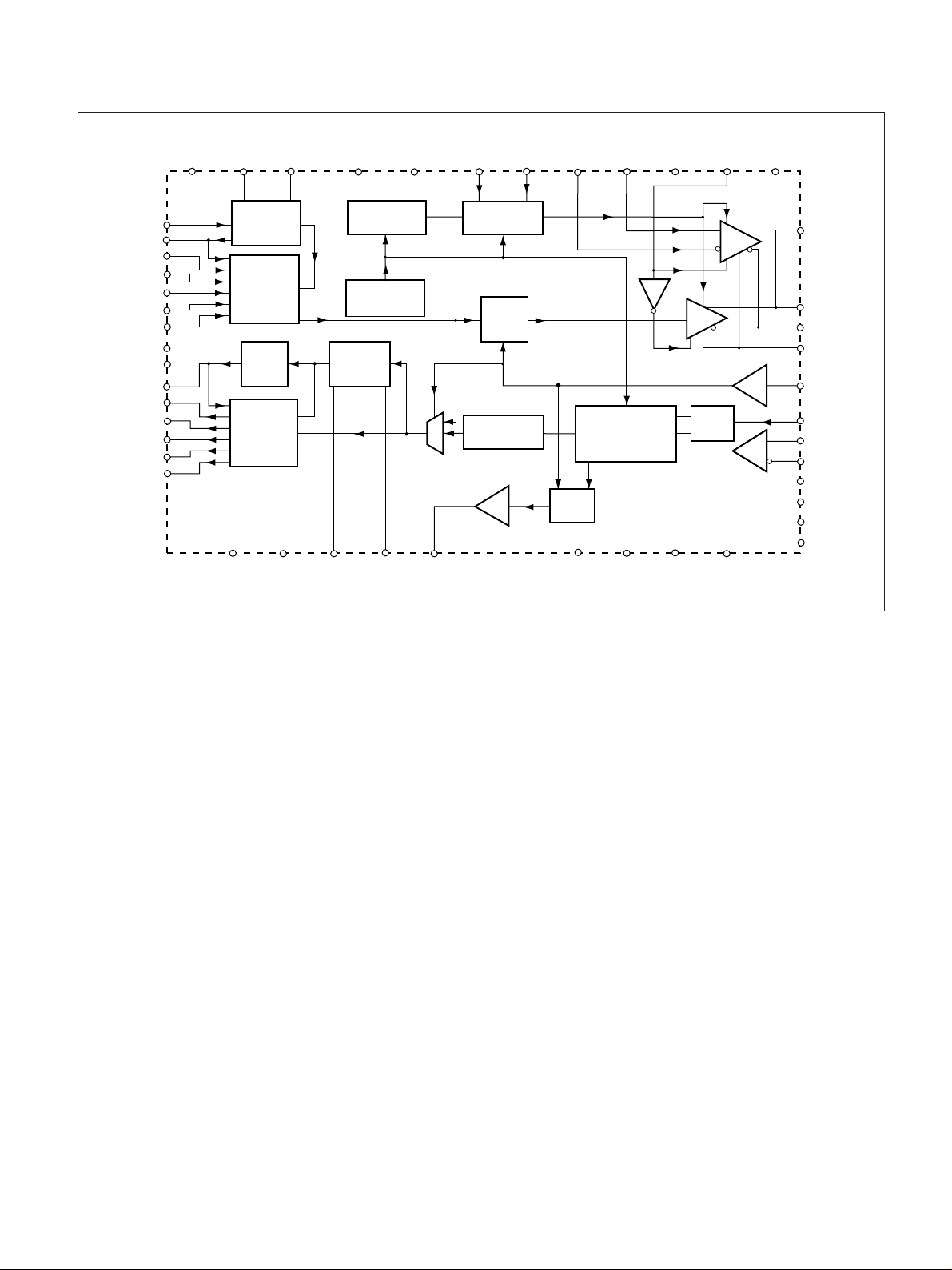
Fig.3 System block diagram
FUNCTIONAL DESCRIPTION
The functional blocks within the device are shown in Fig. 3.
These are described below:-
Transmit Section
Times Five Clock Multiplier 25MHz to 125MHz
This circuit consists of a phase lock loop (PLL) that is
operating at 125MHz, centre frequency. The 125MHz is
divided by 5 to produce a 25MHz clock which is phase
compared with a 25MHz crystal clock reference frequency
which is input on pin REFCLK. The 25MHz clock (pin TXC)
is then sent to the PCS layer to clock in in the 5 bit nibble
data. Pins LFTA and LFTB are provided to set the VCO
characteristics. The recommended loop filter components
are shown in Fig.6.
A control current is derived from the clock multiplier and
is used by the receive clock recovery circuit to centre the
PLL when no input data is present.
Five Bit Nibble to 125MHz Shifter
Data is input to the transmit side in 5 bit wide parallel
form on pins TDAT0 through TDAT4. This NRZ data is
clocked in on the positive edge of the 25MHz clock pin TXC.
The parallel data is first loaded into a 5 bit wide register prior
to being loaded into a 5 bit PISO where it is converted into
a serial data stream. The last stage of the shifter incorporates
a converter to change the data from NRZ to NRZI.
NRZ to MLT3 Encoder
The serial data from the shifter then passes through an
encoder which converts the NRZI binary data into the three
level MLT-3 format for transmission by the 'TXO' outputs.
Transmit Line Drivers
There are two on-chip Line Drivers both of which share
the output pins TXOP and TXON. The N10/100 pin is used
to control which driver is active and allowed to drive the line.
When held high the MLT-3 data is output by the 100Mb/s
driver. This driver consists of differential current source
outputs with programmable sink capability, designed to
drive a nominal output impedance of 50Ω.
Output current is set by the value of an external resistor
) between pin 'TXREF' and 'TXGND'.
(R
REF
This resistor defines an internal reference current derived
from an on-chip bandgap reference.
Final output current at the 'TXO' outputs is a multiple of
this current and is defined as:-
I
(mA) = 52/R
TXO
REF
(kΩ)
Transition times of the 'TXO' outputs are matched and
internally limited to approx. 2.5ns to reduce EMI emissions.
3
Page 4

NWK914D
When N10/100 is held low the 10Mb/s driver is selected.
This 10Mb/s driver consists of a differential analog buffer
designed to take a fully cable conditioned 10Mb/s signal
from the filter output of existing 10BASE-T electronics. The
10BASE-T signal is input on pins 10TXIN and 10TXIP. The
output current of the buffer is determined by the same
external R
resistor on pin TXREF as used for the 100Mb/
REF
s driver.
The unselected driver is switched to a tristated power
save mode. A low voltage shutdown circuit turns off both TX
drivers when V
voltage falls to a level below the specified
CC
minimum.
When operating in single 100Mb/s applications a 1:1
turn ratio magnetics will be used and therefore to attain the
desired line driving current of 40mA out of the secondary a
TXO output drive of 40mA is required. Using the above
formula it will be found that 1.3Ω is the nearest prefered
value to that required to give the 40mA.
In the case of dual 10Mb/s and 100Mb/s applications a
2:1 turn ratio magnetics is recommended. The use of 2:1
magnetics enables a greater efficiency to be gained from
the 10Mb/s driver by using a lower output current. At the
same time this lower current is also true of the 100Mb/s
output where now only a 20mA drive is required. An R
REF
value of 2.6KΩ is used to set this current. Internal current
ratioing within the device will ensure that the correct drive
current is chosen depending upon whether the drives are in
10Mb/s or 100Mb/s mode as selected by pin N10/100.
The R
value can be adjusted to compensate for
REF
different magnetics and board layouts. The object is to
achieve an output level of 2V p-p measured at the RJ45
socket in compliance with 802.3.
When the TXOE pin is held low the TXdrivers are tristated regardless of the mode selected by the N10/100 pin.
Receiver Section
Equalizer
The equalizer circuit is necessary to compensate for
signal degradation due to cable losses, however overequalization must be avoided to prevent excessive overshoots
resulting in errors during the reception of MLT-3 data. Three
operating modes are therefore provided.
These three operating modes are controlled by the state
of tristate input 'EQSEL' and are described below:-
1) Auto Equalization ('EQSEL' floating)
Fully automatic equalization is achieved through the
use of a feedback loop driven by a control signal derived
from the signal amplitude. This provides adaptive control
and prevents over-modulation of the signal when short
cable lengths are used.
2) Full Equalization ('EQSEL' low)
In this mode, full equalization is applied to the input
signal irrespective of amplitude.
3) No Equalization ('EQSEL high)
The equalization circuit is disabled completely during
this mode.
Base Line Wander Correction
MLT-3 codes have significant low frequency components
in their spectrum which are not transmitted through the
transformers that couple the line to the board. This results in
'Base Line Wander', which can significantly reduce the
noise immunity of the receiver.
The purpose ot the correction circuit is to restore these
low frequency components through the use of a feedback
arrangement. The circuit will also correct any DC offset that
may exist on the receive signal.
Signal Detector
A signal detect circuit is provided which continuously
monitors the amplitude of the input signal being received on
pins RXIP and RXIN. After the input signal reaches the
specified level which the equalizer can correctly equalize,
SDT is asserted high. Conversely if the signal level falls
below a limit for reliable operation then SDT will go low.
Comparators MLT-3 to NRZ Decoder
The equalized MLT-3 data is then passed to a set of
window comparators which are used to determine the signal
level. The comparator outputs are OR’ed together to
reconstitute the NRZI data.
PLL Clock Recovery
This function consists of a 125MHz PLL that is locked to
the incoming data stream. The PLL is first centred to the
transmit clock multiplier using an internal analog reference
signal. Once a valid input signal is present, the PLL will lock
to, and thus extract the clock from, the incoming data
stream. Pins LFRA and LFRB are provided to set the VCO
characteristics. The recommended loop filter components
are shown in Fig.6.
125MHz Shifter to Parallel Data
The 125Mb/s serial data stream with an accompanying
phase related 125MHz clock is output from the PLL.
This data stream is clocked into the serial to parallel
register using the 125MHz clock. This data is then latched
prior to being clocked out on pins RDAT0 to RDAT4. A
25MHz clock, derived from the 125MHz PLL by a divide by
5, is used to clock the parallel data and is output to pin RXC.
Loopback Logic
Pin ‘LBEN’ controls loopback operation. A low level on
this pin defines normal operation, a high level defines
loopback mode. In loopback mode, the transmit data is
internally routed to the receive circuitry, SDT is forced high
and the TXOP and TXON outputs are disabled.
Test Pins and No-Connects
Two pins are provided on the product to aid testing in
production. These pins TEST(38), and TESTIP(37) must be
left unconnected for normal operation in application circuits.
Additionally, there are four No-Connect pins (2,3,7,8)
which also mustt be left unconnected for normal operation.
4
Page 5

NWK914D
AC CHARACTERISTICS
Recommended operating conditions apply except where stated.
Characteristic Units Conditions
AC characteristics
100Mb/s TX driver outputs rise/fall times - 2.5 - ns 100Ω differential load
pins TXOP, TXON measured at RJ45
REFCLK frequency 1 - 25 - MHz
REFCLK tolerance 2 - 100 - ppm
REFCLK M/S ratio 3 40:60 - 60:40 %
REFCLK to TXC 4 5 - 13 ns Tx PLL in lock
propagation delay
TDAT0 → 4 to TXC setup time 5 12 - - ns
TDAT0 → 4 to TXC hold time 6 0 - - ns
RDAT0 → 4 valid to RXC +Ve edge 7 10 - - ns
RXC to RDAT0 → 4 invalid 8 10 - - ns
RXC M/S ratio 9 45:55 - 55:45 %
REFCLK to SDT transition 5 - 15 ns
NOTE: Conditions for AC Characteristics:
All AC measurementsare made at aVth + 1.5V and with TTL output loaded with 25pf
Waveform Value
Timing Min. Typ. Max.
REFCLK
TXC
TDAT
0 →4
TXO
RXC
RDAT
0 →4
4
VALID
DATA
31
2
bit 4 bit 3
Fig.4 Transmit timing waveform
9
5
VALID
DATA
8
bit 2 bit 1 bit 0
5
VALID
DATA
6
bit 4
Fig.5 Receive timing waveform
5
Page 6

NWK914D
Pin Name Pin Type Pin Number Pin Description
SYMBOL Interface
RXC TTLOP 4 25MHz recovered receive clock. This is aligned with and used to clock
SDT TTLOP 5 Signal detect output. This output is high when an input signal of sufficient
TDAT4 TTLIP 40 The 100BASE-TX transmit input bit 4
TDAT3 TTLIP 41 The 100BASE-TX transmit input bit 3
TDAT2 TTLIP 42 The 100BASE-TX transmit input bit 2
TDAT1 TTLIP 43 The 100BASE-TX transmit input bit 1
TDAT0 TTLIP 44 The 100BASE-TX transmit input bit 0
TXC TTLOP 47 25MHz transmit clock. This is aligned with and used to clock in the 5 bit parallel
RDAT0 TTLOP 48 The 100BASE-TX receive output bit 0
RDAT1 TTLOP 49 The 100BASE-TX receive output bit 1
RDAT2 TTLOP 50 The 100BASE-TX receive output bit 2
RDAT3 TTLOP 51 The 100BASE-TX receive output bit 3
RDAT4 TTLOP 52 The 100BASE-TX receive output bit 4
Network Interface
RXIP analog input 15 + Differential receive signal input from magnetics
RXIN analog input 16 – Differential receive signal input from magnetics
TXON analog output 22 – Differential transmit line driver outputs to magnetics
TXOP analog output 23 + Differential transmit line driver outputs to magnetics
10BASE-T Interface
10TXIN analog input 19 The filtered 10BASE-T transmit input (–)
10TXIP analog input 20 The filtered 10BASE-T transmit input (+)
Control Pins
N10/100 TTLIP 36 10/100 mode selection. A low selects the 10BASE-T mode and enables the
EQSEL 3 level IP 18 Mode select input for equalizer. Normally this pin is left unconnected (floating) for
LBEN TTLIP 35 Loopback enable input. A high on this pin selects the loopback mode and low selects
TXOE TTLIP 33 Transmit output enable. A high on this pin selects normal operation. A low on this
TESTIP test 37 Test pin. This pin must be left unconnected for proper operation.
TEST test 38 Test pin. This pin must be left unconnected for proper operation.
N/C 2,3,7,8 No connection. This pin must be left unconnected for proper operation.
Component Connections
REFCLK TTLIP 45 25MHz clock input. An external 25MHz oscillator is input to this pin.
TXREF analog input 25 TXOP/N line driver current setting pin. Connects to TXGND through a resistor.
LFRB analog 10 Differential loop filter pin for receive PLL (see fig.6)
LFRA analog 11 Differential loop filter pin for receive PLL (see fig.6)
LFTB analog 30 Differential loop filter pin for transmit clock PLL (see fig.6)
LFTA analog 31 Differential loop filter pin for transmit clock PLL (see fig.6)
Power
TTLGND Power 1,39 GND for TTL logic I/Os
RDLV
CC
RXPLLGND Power 9 GND to receive PLL
RXPLLV
RXVCC2 Power 13 +5V supply to adaptive equalizer and QFB circuits
CC
Power 6 +5V supply to receive logic
Power 12 +5V supply to receive PLL
RXGND Power 14 GND to to adaptive equalizer and QFB circuits
RXVCC1 Power 17 +5V supply to MLT-3 to NRZI converter
TXV
CC
TXGND Power 24 GND to transmit line driver circuits
RXV
CC
SUBGND Power 27 Chip substrate GND connection
Power 21 +5V supply to transmit line driver circuits
Power 26 +5V supply to on-chip bandgap reference
BGAPGND Power 28 GND to on-chip bandgap reference
TXPLLGND Power 29 GND to to transmit clock-multiplier PLL
TXPLLV
TDLV
CC
TXLV
CC
CC
Power 32 +5V supply to transmit clock-multiplier PLL
Power 34 +5V supply to transmit logic
Power 46 +5V supply to TTL logic I/Os
6
out the 5 bit parallel receive data to the PCS layer.
amplitude is detected on the RXI inputs.
100BASE-TX transmit data from the PCS layer.
data on pins 10TXIP/N to be outut on the TXOP/N pins. A high selects the
100BASE-TX mode, enabling the 100Mb/s drivers.
auto-eq. mode. High selects minimum equalization. Low selects full equalization.
normal operation.
pin puts both of the TX drivers in tri-state mode.
Table 1: Pin descriptions
Page 7

NWK914D
PCS
or
MAC
(with
embedded
PCS)
Xtal Osc.
5
5
100pF
LFTA
REFCLK
TDAT0-4
TXC
RXC
RDAT0-4
6.2KΩ
1KΩ
R1
C1
LFRBLFRA
R3
.033µF
C2
LFTB
TXREF
NWK914D
C3
.01µF
See Table 2 for
these resistor values
R2
TXGND
TXOP
TXON
RXIP
RXIN
Fig.6 Simplified 100BASE-TX system block diagram showing NWK914D external components
REF. VALUE TOL. FUNC. NOTES
C1 100pF 20% loop fltr
C2 0.033µF 20% loop fltr
C3 .01µF 20% loop fltr
R1 1KΩ 1% loop fltr
R2 1300Ω 1% tx ref 1:1 magnetics
R3 6.2KΩ 1% loop fltr
R5,R6 50Ω 1% xmit 1:1 magnetics
R7,R8 15Ω 1% rcv pad
R9 68Ω 1% rcv pad
R2 2.6KΩ 1% tx ref 2:1 magnetics
R5,R6 200Ω 1% xmit 2:1 magnetics
CT on transformer connects directly to 2:1 magnetics
with C4 omitted
TX V
CC
Table 2: External components
TxV
cc
R5
R9
15Ω
68Ω
15Ω
R6
0.1µF
R7
R8
C4
CT
1:1
M
A
G
N
E
T
I
C
S
RJ45
EXTERNAL REQUIREMENTS
The NWK914D requires a number of external components
for the device to function correctly and these are shown in
the simplified 100BASE-TX application circuit in Fig.6 and
the component value information given in Table 2.
Note that the values of R2, R5 and R6 vary depending
upon application. When using 1:1 magnetics, use the values
shown in the middle of Table 2 with note "1:1 magnetics".
When using 2:1 magnetics use the values shown in the last
two lines of Table 2. Please refer to the Transmit Line Driver
section on pages 3-4 for more information on these values.
For more detailed Application information please contact
your local Sales Office.
GLOSSARY OF TERMS AND ABREVIATIONS
MAC Media Access Control
MLT-3 Multi Level Transmit -3 levels
NRZ Non Return To Zero
NRZI Non Return to Zero Inverse
PCS Physical Coding Sublayer
PHY PHYsical Layer
PLL Phase Locked Loop
PMD Physical Media Dependent
UTP Unshielded Twisted Pair
RX Receive
STP Shielded Twisted Pair
TX Transmit
UTP Unshielded Twisted Pair
VCO Voltage Controlled Oscillator
NWK914B NWK914S NWK914D
Base Line Wander Correction - improved to 100m improved to 100m
TXREF resistor with 1:1 magnetics 620Ω 680Ω 1300Ω
Table 3: Differences between NWK914B, NWK914S and NWK914D
7
Page 8
Page 9

http://www.mitelsemi.com
World Headquarters - Canada
Tel: +1 (613) 592 2122
Fax: +1 (613) 592 6909
North America Asia/Pacific Europe, Middle East,
Tel: +1 (770) 486 0194 Tel: +65 333 6193 and Africa (EMEA)
Fax: +1 (770) 631 8213 Fax: +65 333 6192 Tel: +44 (0) 1793 518528
Fax: +44 (0) 1793 518581
Information relating to products and services furnished herein by Mitel Corporation or its subsidiaries (collectively “Mitel”) is believed to be reliable. However, Mitel assumes no
liability for errors that may appear in this publication, or for liability otherwise arising from the application or use of any such information, product or service or for any infringement of
patents or other intellectual property rights owned by third parties which may result from such application or use. Neither the supply of such information or purchase of product or
service conveys any license, either express or implied, under patents or other intellectual property rights owned by Mitel or licensed from third parties by Mitel, whatsoever.
Purchasers of products are also hereby notified that the use of product in certain ways or in combination with Mitel, or non-Mitel furnished goods or services may infringe patents or
other intellectual property rights owned by Mitel.
This publication is issued to provide information only and (unless agreed by Mitel in writing) may not be used, applied or reproduced for any purpose nor form part of any order or
contract nor to be regarded as a representation relating to the products or services concerned. The products, their specifications, services and other information appearing in this
publication are subject to change by Mitel without notice. No warranty or guarantee express or implied is made regarding the capability, performance or suitability of any product or
service. Information concerning possible methods of use is provided as a guide only and does not constitute any guarantee that such methods of use will be satisfactory in a specific
piece of equipment. It is the user’s responsibility to fully determine the performance and suitability of any equipment using such information and to ensure that any publication or
data used is up to date and has not been superseded. Manufacturing does not necessarily include testing of all functions or parameters. These products are not suitable for use in
any medical products whose failure to perform may result in significant injury or death to the user. All products and materials are sold and services provided subject to Mitel’s
conditions of sale which are available on request.
M Mitel (design) and ST-BUS are registered trademarks of MITEL Corporation
Mitel Semiconductor is an ISO 9001 Registered Company
Copyright 1999 MITEL Corporation
All Rights Reserved
Printed in CANADA
TECHNICAL DOCUMENTATION - NOT FOR RESALE
 Loading...