

Page 1

NTE948 & NTE948SM
Integrated Circuit
Quad Operational Amplifier
Description:
The NTE948 (14–Lead DIP) and NTE948SM (SOIC–14) consists of four independent, high gain, internally compensated, low power operational amplifiers which have been designed to provide functional characteristics identical to those of the familiar 741 operational amplifier.
Features:
• Low Supply Current Drain
• Class AB Output Stage – No Crossover Distortion
• Low Input Offset Voltage
• Low Input Offset Current
• Low Input Bias Current
• High Degree of Isolation Between Amplifiers
• Overload Protection for Inputs and Outputs
• Available in 14–Lead DIP (NTE948) and Surface Mount (NTE948SM)
Absolute Maximum Ratings:
Supply Voltage, V
S
±18V. . . . . . . . . . . . . . . . . . . . . . . . . . . . . . . . . . . . . . . . . . . . . . . . . . . . . . . . . . . . . . . .
Differential Input Voltage ±36V. . . . . . . . . . . . . . . . . . . . . . . . . . . . . . . . . . . . . . . . . . . . . . . . . . . . . . . . . . .
Output Short Circuit Duration (Note 1) Continuous. . . . . . . . . . . . . . . . . . . . . . . . . . . . . . . . . . . . . . . . .
Power Dissipation (T
Maximum Junction Temperature, T
Operating Ambient Temperature Range, T
Storage Temperature Range, T
Thermal Resistance, Junction–to–Ambient (Note 2), R
= +25°C, Note 2), P
A
J
stg
D
750mW. . . . . . . . . . . . . . . . . . . . . . . . . . . . . . . . . . . . . . .
+100°C. . . . . . . . . . . . . . . . . . . . . . . . . . . . . . . . . . . . . . . . . . . . . . .
A
0° to +70°C. . . . . . . . . . . . . . . . . . . . . . . . . . . . . . . . . . . . .
–65° to +150°C. . . . . . . . . . . . . . . . . . . . . . . . . . . . . . . . . . . . . . . . . .
thJA
100°C/W. . . . . . . . . . . . . . . . . . . . . . . . . .
Note 1. Any of the amplifier outputs can be shorted to ground indefinitely; however, more than one
should not b e s imultaneously s horted a s t he maximum junction t emperature w ill b e exceeded.
Note 2. The maximum power dissipation for these devices must be derated at elevated tempera-
R
tures and is dicated by T
J(MAX),
able power dissipation at any temperature is P
, and the ambient temperature, TA. The maximum avail-
thJA
= (T
D
J(MAX)
– TA)/R
or the 25°C P
thJA
D(MAX)
which ever is less.
,
Page 2
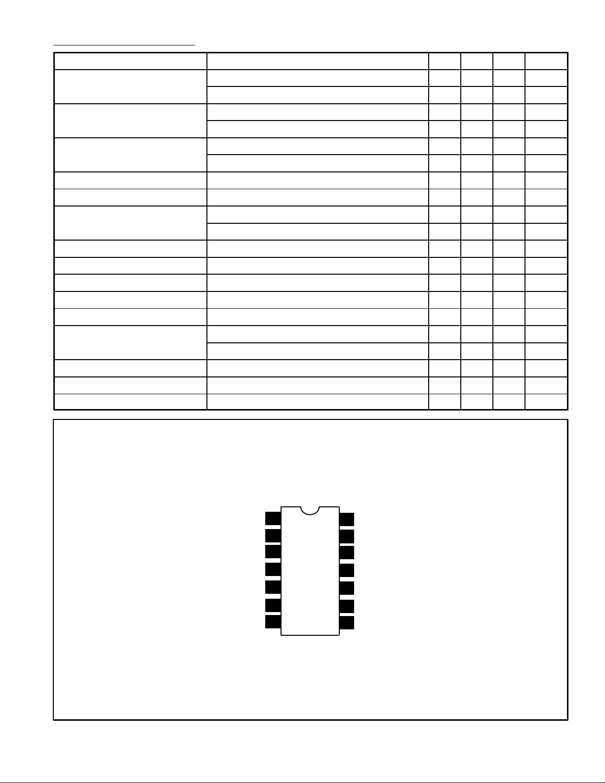
Electrical Characteristics: (VS = ±15V, 0° ≤ TA ≤ +70°C unless otherwise specified)
Parameter Test Conditions Min Typ Max Unit
Input Offset Voltage TA = +25°C, RS ≤ 10kΩ – 1.0 6.0 mV
RS ≤ 10kΩ – – 7.5 mV
Input Offset Current TA = +25°C – 4 50 nA
– – 100 nA
Input Bias Current TA = +25°C – 30 200 nA
– – 400 nA
Input Resistance TA = +25°C 0.8 2.5 – MΩ
Supply Current, All Amplifiers TA = +25°C, VS = ±15V – 2.4 4.5 mA
Large Signal Voltage Gain TA = +25°C, VS = ±15V, V
VS = ±15V, V
Amplifier–to–Amplifier Coupling TA = +25°C, f = 1Hz to 20kHz – –120 – dB
Small–Signal Bandwidth TA = +25°C – 1.0 – MHz
Phase Margin TA = +25°C, AV = 1 – 60 – degrees
Slew Rate TA = +25°C, AV = 1 – 0.5 – V/µs
Output Short–Circuit Current TA = +25°C – 25 – mA
Output Voltage Swing VS = ±15V, RL = 10kΩ ±12 ±13 – V
VS = ±15V, RL = 2kΩ ±10 ±12 – V
Input Voltage Range VS = ±15V ±12 – – V
Common–Mode Rejection Ratio RS ≤ 10kΩ 70 90 – dB
Supply Voltage Rejection Ratio RS ≤ 10kΩ, ±5V ≤ VS ≤ ±15V 77 96 – dB
= ±10V, R
OUT
Pin Connection Diagram
= ±10V, RL ≥ 2kΩ 25 160 – V/mV
OUT
> 2kΩ – – 15 V/mV
L
Output A
Invert Input A
Non–Invert Input A
V (+)
Non–Invert Input B
Invert Input B
Output B
1
2
3
4
5
6
7
Output D
14
13
Invert Input D
Non–Invert Input D
12
V (–)
11
Non–Invert Input C
10
9
Invert Input C
8
Output C
Page 3

NTE948
14 8
17
14
.785 (19.95)
Max
.200 (5.08)
Max
.100 (2.45) .099 (2.5) Min
.600 (15.24)
NTE948SM
.340 (8.64)
8
(5.99)
.300
(7.62)
.236
1
.050 (1.27)
NOTE: Pin1 on Beveled Edge
7
.006 (.152)
.154
(3.91)
016
(.406)
061
(1.53)
.198 (5.03)
 Loading...