

Page 1

NTE941S
Integrated Circuit
Operational Amplifier
Description:
The NTE941S is a general purpose operational amplifier in a 7–Lead SIP type package and offers
many features which make its application nearly foolproof: overload protection on the input and output, no latch–up when the common mode range is exceeded, as well as freedom from oscillators.
Absolute Maximum Ratings:
Supply Voltage, V
Differential Input Voltage, V
Common Mode Input Voltage (Note 2), V
Power Dissipation (Note 1), P
Output Short–Circuit Duration, t
Operating Temperature Range, T
Storage Temperature Range, T
Junction Temperature, T
S
ID
ICM
D
S
opr
stg
J
Lead Temperature (During Soldering, 10sec), T
Thermal Resistance, Junction–to–Ambient, R
thJA
Continuous. . . . . . . . . . . . . . . . . . . . . . . . . . . . . . . . . . . . . . . . . . . . . .
0° to +70°C. . . . . . . . . . . . . . . . . . . . . . . . . . . . . . . . . . . . . . . . . . .
–65° to +150°C. . . . . . . . . . . . . . . . . . . . . . . . . . . . . . . . . . . . . . . . . .
L
±18V. . . . . . . . . . . . . . . . . . . . . . . . . . . . . . . . . . . . . . . . . . . . . . . . . . . . . . . . . . . . . . . .
±30V. . . . . . . . . . . . . . . . . . . . . . . . . . . . . . . . . . . . . . . . . . . . . . . . . . . . . . .
±15V. . . . . . . . . . . . . . . . . . . . . . . . . . . . . . . . . . . . . . . . . .
500mW. . . . . . . . . . . . . . . . . . . . . . . . . . . . . . . . . . . . . . . . . . . . . . . . . . .
+100°C. . . . . . . . . . . . . . . . . . . . . . . . . . . . . . . . . . . . . . . . . . . . . . . . . . . . . . . . .
+260°C. . . . . . . . . . . . . . . . . . . . . . . . . . . . . . . . . . . .
+100°C/W. . . . . . . . . . . . . . . . . . . . . . . . . . . . . . . . .
Note 1. For operation at elevated temperatures, these devices must be derated based on thermal
resistance, and T
Max (TJ = TA + (R
J
thJA PD
).
Note 2. For supply voltage less than ±15V , the absolute maximum input voltage is equal to the supply
voltage.
Page 2
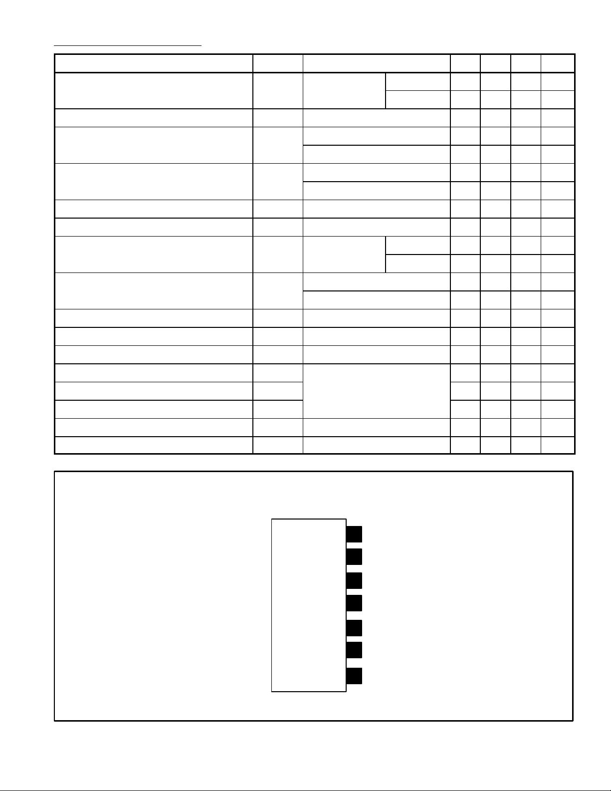
Electrical Characteristics: (VS = ±15V, 0° ≤ TA ≤ +70°C unless otherwise specified)
Parameter Symbol Test Conditions Min Typ Max Unit
Input Offset Voltage V
IO
RS ≤ 10kΩ TA = +25°C – 2.0 6.0 mV
– – 7.5 mV
Input Offset Voltage Adjustment Range V
Input Offset Current I
IOR
IO
VS = ±20V, TA = +25°C – ±15 – V
TA = +25°C – 20 200 nA
– – 300 nA
Input Bias Current I
IB
TA = +25°C – 80 500 nA
– – 0.8 µA
Input Resistance r
Common Mode Input Voltage Range V
Large Signal Voltage Gain A
Output Voltage Swing V
ICR
VS = ±20V, TA = +25°C 0.3 2.0 – MΩ
i
TA = +25°C – ±12 ±13 V
VO = ±10V,
V
RL ≥ 2kΩ
RL ≥ 10kΩ ±12 ±14 – V
O
TA = +25°C 20 200 – V/mV
15 – – V/mV
RL ≥ 2kΩ ±10 ±13 – V
Output Short–Circuit Current I
OS
TA = +25°C – 25 – mA
Common–Mode Rejection Ratio CMRR RS ≤ 10kΩ, VCM = ±12V 70 90 – dB
Supply Voltage Rejection Ratio PSRR VS = ±20V to ±5V, RS ≤ 10kΩ 77 96 – dB
Transient Response Rise Time t
TLH
TA = +25°C, Unity Gain – 0.3 – µs
Transient Response Overshoot os – 5 – %
Transient Response Slew Rate SR – 0.5 – V/µs
Supplu Current I
Power Consumption P
Pin Connection Diagram
D
TA = +25°C – 1.7 2.8 mA
TA = +25°C – 50 85 mW
C
(Front View)
V (+)
7
Output
6
Offset Null
5
4
V (–)
3 Non–Inverting Input
2 Inverting Input
Offset Null
1
Page 3

.128 (3.2)
.700 (17.8) Max
.099
(2.5)
Min
.323
17
.100 (2.54).012 (0.25)
.600 (15.24)
(8.2)
Max
 Loading...