

Page 1

NTE5440
Silicon Controlled Rectifier (SCR)
800V, 10A, Isolated Tab
Applications:
D Temperature Control
D Motor Control
D Transformerless Power Supply Regulators
D Relay and Coil Pulsing
D Power Supply Crowbar Protection
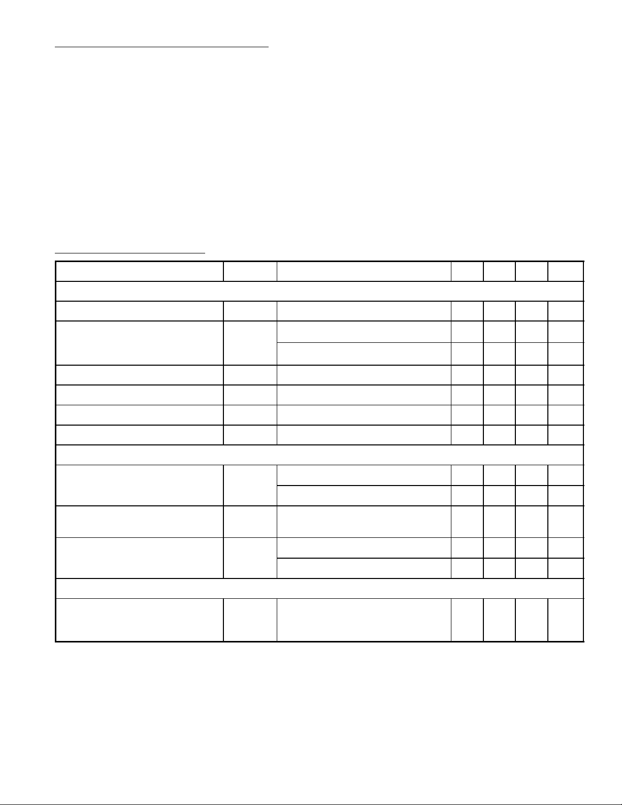
Absolute Maximum Ratings:
Anode to Cathode
Non–Repetitive Peak Voltages (t ≤ 10ms, Note 1), V
Repetitive Peak Voltages (δ ≤ 0.01), V
Peak Working Voltages, V
Continuous Voltages, VD, V
Average On–State Current, I
DWM
R
T(AV)
, V
RWM
DRM
, V
RRM
(Averaged over any 20ms period) up to Th = +74°C 5.7A. . . . . . . . . . . . . . . . . . . . . . . . . . .
RMS On–State Current, I
Repetitive Peak On–State Current, I
Non–Repetitive Peak On–State Current, I
T(RMS)
TRM
TSM
(t = 10ms, Half–Sinewave, TJ = +110°C prior to surge, with Reapplied V
I2t for Fusing (t = 10ms), I2t 50A2s. . . . . . . . . . . . . . . . . . . . . . . . . . . . . . . . . . . . . . . . . . . . . . . . . . . . .
Rate of Rise of On–State Current after Triggering, dIT/dt
(IG = 50mA to IT = 20A, dIG/dt = 50mA/µs) 50A/µs. . . . . . . . . . . . . . . . . . . . . . . . . . . . . . . . .
Gate to Cathode
Reverse Peak Voltage, V
RGM
Average Power Dissipation (Averaged over any 20ms period), P
Peak Power Dissipation, P
GM
Temperatures
Operating Junction Temperature, T
Storage Temperature Range, T
J
stg
Maximum Lead Temperature (During Soldering, less than 5sec) +275°C. . . . . . . . . . . . . . . . . . . .
DSM
, V
RSM
RWMmax
G(AV)
–40° to +125°C. . . . . . . . . . . . . . . . . . . . . . . . . . . . . . . . . . . . . . .
800V. . . . . . . . . . . . . . . . . . . . . .
800V. . . . . . . . . . . . . . . . . . . . . . . . . . . . . . . . . . .
400V. . . . . . . . . . . . . . . . . . . . . . . . . . . . . . . . . . . . . . . . . . . .
400V. . . . . . . . . . . . . . . . . . . . . . . . . . . . . . . . . . . . . . . . . . . . . . . . . . . .
9A. . . . . . . . . . . . . . . . . . . . . . . . . . . . . . . . . . . . . . . . . . . . . . . . . . . .
65A. . . . . . . . . . . . . . . . . . . . . . . . . . . . . . . . . . . . . . . . . . . .
) 100A.
5V. . . . . . . . . . . . . . . . . . . . . . . . . . . . . . . . . . . . . . . . . . . . . . . . . . . . . .
500mW. . . . . . . . . . . . . . .
5W. . . . . . . . . . . . . . . . . . . . . . . . . . . . . . . . . . . . . . . . . . . . . . . . . . . . .
+110°C. . . . . . . . . . . . . . . . . . . . . . . . . . . . . . . . . . . . . . . . . . . .
Note 1. Although not recommended, higher Off–State voltages may be applied without damage, but
the thyristor may switch into the On–State. The Rate–of–Rise of On–State current should
not exceed 15A/µs.
Page 2
Absolute Maximum Ratings (Cont’d):
Isolation:
Minimum From all Three Pins to External Heatsink (Peak), V
Typical Capacitance from Anode to External Heatsink, C
Thermal Characteristics:
Thermal Resistance from Junction to External Heatsink, R
With Heatsink Compound 4.5K/W. . . . . . . . . . . . . . . . . . . . . . . . . . . . . . . . . . . . . . . . . . . . . . .
Without Heatsink Compound 6.5K/W. . . . . . . . . . . . . . . . . . . . . . . . . . . . . . . . . . . . . . . . . . . .
Thermal Resistance from Junction–to–Ambient in Free Air, R
(Mounted on a printed circuit board at a = any lead length
and with copper laminate, Note 2) 55K/W. . . . . . . . . . . . . . . . . . . . . . . . . . . . . . . . . . . . . . . .
isol
isol
thj–h
1000V. . . . . . . . . . . . . . . . . . . . .
12pf. . . . . . . . . . . . . . . . . . . . . . . . . . .
thJA
Note 2. The quoted values of R
should be used only when no leads of other dissipating compo-
thJA
nents run to the same tie–point.
Electrical Characteristics: (TJ = +110°C unless otherwise specified)
Parameter Symbol Test Conditions Min Typ Max Unit
Anode to Cathode
On–State Voltage V
Rate of Rise of Off–State dVD/dt
Voltage that will not
Trigger any Device
Reverse Current I
Off–State Current I
Latching Current I
Holding Current I
R
D
L
H
Gate to Cathode
Gate–Trigger Voltage V
GT
IT = 23A, TJ = 25°C, Note 3 – – 1.75 V
T
RGK = Open Circuit – – 50 V/µs
RGK = 100Ω
VR = 400V – – 0.5 mA
VD = 400V – – 0.5 mA
TJ = 25°C – – 40 mA
TJ = 25°C – – 20 mA
VD = 6V, TJ = 25°C 1.5 – – V
VD = 6V, TJ = –40°C 2.3 – – V
– – 200 V/µs
Voltage that will not
V
GD
VD = 800V – – 250 mV
Trigger any Device
Gate–Trigger Current I
GT
VD = 6V, TJ = 25°C 15 – – mA
VD = 6V, TJ = –40°C 20 – – mA
Switching Characteristice
Gate–Controlled Turn–On Time
(t
= td + tr) when Switched
gt
from V
= 800V to IT = 40A
D
t
gt
IGT = 100mA, dIg/dt = 5A/µs,
T
= 25°C
J
Note 3. Measured under pulse conditions to avoid excessive dissipation.
– 2 – µs
Page 3

.402 (10.2) Max
.173 (4.4) Max
.224 (5.7) Max
.295
(7.5)
.669
(17.0)
Max
.531
(13.5)
Min
.114 (2.9) Max
.122 (3.1)
Dia
.165
(4.2)
KAG
.100 (2.54) .059 (1.5) Max
NOTE: Tab is isolated
 Loading...