

Page 1

NTE2764
Integrated Circuit
NMOS, 64K Erasable EPROM, 200ns
Description:
The NTE2764 is a 65,536–bit (8192 X 8 bit) Ultraviolet Erasable and Electrically Programmable
Read–Only Memory (EPROM) in a 28–Lead DIP type package which operates from a single +5V supply, making it ideal for microprocessor applications. It features an output enable control and offers
a standby mode with an attendant 67% savings in power consumption.
A distinctive feature of the NTE2764 is a separate output control, output enable (OE) from the chip
enable control (CE). The OE control eliminates bus contention in multiple–bus microprocessor systems. The NTE2764 features fast, simple one–pulse programming controlled by TTL–level signals.
Total programming time for all 65,536 bits is 420 seconds.
Features:
D Ultraviolet Erasable and Electrically Programmable
D Access Time: 250ns Max
D Single Location Programming
D Programmable with Single Pulse
D Low Power Dissipation: 150mA Max (Active Current)
50mA Max (Standby Current)
D Input/Output TTL Compatible for Reading and Programming
D Single +5V Power Supply
D Three–State Outputs
Absolute Maximum Ratings: (TA = +25°C, Note 1 unless otherwise specified)
Supply Voltage, V
Supply Voltage, V
Output Voltage, V
Input Voltage, V
CC
PP
OUT
IN
Operating Temperature Range, T
Storage Temperature Range, T
stg
opr
–0.6 to +6V. . . . . . . . . . . . . . . . . . . . . . . . . . . . . . . . . . . . . . . . . . . . . . . . . . . . . . . . .
–0.6 to +22V. . . . . . . . . . . . . . . . . . . . . . . . . . . . . . . . . . . . . . . . . . . . . . . . . . . . . . . .
–0.6 to +6V. . . . . . . . . . . . . . . . . . . . . . . . . . . . . . . . . . . . . . . . . . . . . . . . . . . . . . . .
–0.6 to +6V. . . . . . . . . . . . . . . . . . . . . . . . . . . . . . . . . . . . . . . . . . . . . . . . . . . . . . . . . . .
–10°C to +80°C. . . . . . . . . . . . . . . . . . . . . . . . . . . . . . . . . . . . . . .
–65°C to +125°C. . . . . . . . . . . . . . . . . . . . . . . . . . . . . . . . . . . . . . . .
Note 1. Exposing the device to stresses above those listed in Absolute Maximum Ratings could
cause permanent damage. The device is not meant to be operated under conditions outside
the limits described in the operational sections of this specification. Exposure to absolute
maximum rating conditions for extended periods may affect device reliability.
Page 2
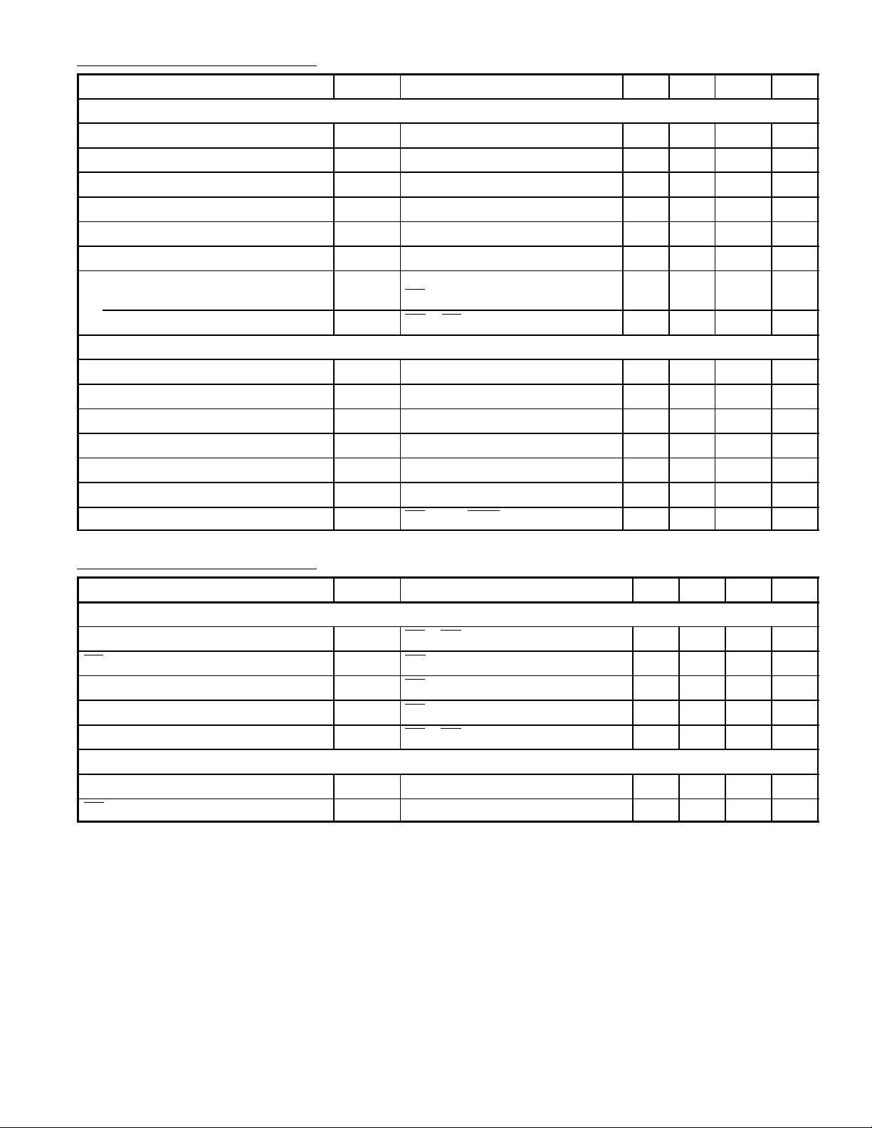
DC Electrical Characteristics: (VCC = +5V ±5% unless otherwise specified)
Parameter Symbol Test Conditions Min Typ Max Unit
Read Mode and Standby Mode (TA = 0° to +70°C)
Output High Voltage V
Output Low Voltage V
Input High Voltage V
Input Low Voltage V
Output Leakage Current I
Input Leakage Current I
LO
IOH = –400µA 2.4 – – V
OH
IOL = 2.1mA – – 0.45 V
OL
IH
IL
V
= 5.25V – – 10 µA
OUT
VIN = 5.25V – – 10 µA
LI
2.0 – VCC +1 V
–0.1 – +0.8 V
VCC Current
Standby I
Active I
CC1
CC2
CE = V
IH
OE = CE = V
– – 50 mA
IL
– – 150 mA
Program, Program Verify, and Program Inhibit Mode (TA = +25° ±5°C, VPP = +21V ±0.5V)
Input High Voltage V
Input Low Voltage V
Input Leakage Current I
Output High Voltage V
Output Low Voltage V
VCC Current I
VPP Current I
IH
LI
OH
OL
CC
PP
IL
VIN = VIL or V
IN
IOH = –400µA 2.4 – – V
IOL = 2.1mA – – 0.45 V
CE = VIL, PGM
IL – – 30 mA
= V
2.0 – VCC +1 V
–0.1 – +0.8 V
– – 10 µA
– – 150 mA
AC Electrical Characteristics: (VCC = +5V ±5% unless otherwise specified)
Parameter Symbol Test Conditions Min Typ Max Unit
Read Mode and Standby Mode (TA = 0° to +70°C, Note 2)
Address to Output Delay t
CE to Output Delay t
Output Enable to Output Delay t
Output Enable High to Output Float t
Address to Output Hold t
ACC
CE
OE
DF
OH
CE = OE = V
OE = V
CE = V
CE = V
IL
IL
IL
CE = OE = V
IL
– – 250 ns
– – 250 ns
10 – 100 ns
0 – 90 ns
IL
0 – – ns
Read Mode and Standby Mode (TA = +25°C ±5°C, VPP = +21V ±5V, Note 3)
Address Setup Time t
OE Setup Time t
AS
OES
2 – – µs
2 – – µs
Note 2. Test Conditions:
Output Load: 1 TTL gate and CL = 100pF
Input Rise and fall Times: 20ns
Input Pulse Levels: 0.8V to 2.2V
Timing Measurement Reference Level:
Inputs: 1.0V and 2.0V
Outputs: 0.8V and 2.0V
Note 3. Test Conditions:
Input Pulse Levels: 0.8V to 2.2V
Input Timing Reference Level: 1.0V and 2.0V
Output Timing Reference Level: 0.8V and 2.0V
Input Rise and fall Times: 20ns
Page 3
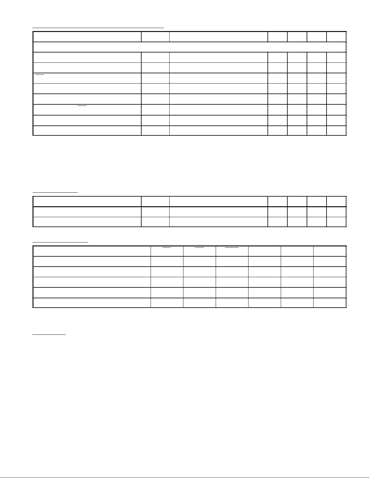
AC Electrical Characteristics (Cont’d): (VCC = +5V ±5% unless otherwise specified)
Parameter Symbol Test Conditions Min Typ Max Unit
Read Mode and Standby Mode (Cont’d) (TA = +25°C ±5°C, VPP = +21V ±5V, Note 3)
Data Setup Time t
Address Hold Time t
CE Setup Time t
Data Hold Time t
Chip Enable to Output Float Delay t
Data Valid from OE t
Program Pulse Width t
VPP Setup Time t
DS
AH
CES
DH
DF
OE
PW
VS
Note 3. Test Conditions:
Input Pulse Levels: 0.8V to 2.2V
Input Timing Reference Level: 1.0V and 2.0V
Output Timing Reference Level: 0.8V and 2.0V
Input Rise and fall Times: 20ns
Capacitance: (TA = +25°C, f = 1MHz unless otherwise specified)
Parameter Symbol Test Conditions Min Typ Max Unit
Input Capacitance C
Output Capacitance C
OUT
VIN = 0V – – 6 pF
IN
V
= 0V – – 12 pF
OUT
2 – – µs
0 – – µs
2 – – µs
2 – – µs
0 – 130 ns
–
–
150 ns
45 50 55 ms
2 – – µs
Mode Selection: (Note 4)
Mode CE OE PGM V
Read V
Stanby V
Program V
Program Verify V
Program Inhibit V
IH
IH
PP
IL
V
IL
X X V
IL
IL
X V
V
IL
X X V
V
IH
IL
V
IH
V
CC
CC
V
PP
V
PP
PP
V
CC
V
CC
V
CC
V
CC
V
CC
V
CC
O0 – O
D
OUT
High Z
D
IN
D
OUT
High Z
7
Note 4. X can be either VIL or VIH.
Function:
The N TE2764 operates f rom a s ingle + 5V p ower s upply , m aking it i deal f or m icroprocessor a pplicati ons.
Programming of the NTE2764 is achieved with a single 50ms TTL pulse. Total programming time for
all 65,536 bits is 420 sec. Due to the simplicity of the programming requirements, devices on boards
and in systems may be easily programmed without any special programmer.
The NTE2764 features a standby mode which reduces the power dissipation from a maximum active
power dissipation of 788mW to a maximum standby power dissipation of 262mW. This results in a
67% savings with no increase in access time.
Erasure of the NTE2764 programmed data can be attained when exposed to light with wavelengths
shorter than approximately 4,000 Angstroms. It should be noted that constant exposure to direct sunlight or room level fluorescent lighting could erase the NTE2764. Consequently, if the NTE2764 is
to be exposed to these types of lighting conditions for long periods of time, its window should be
masked to prevent unintentional erasure.
Page 4

Function (Cont’d):
The recommended erasure procedure for the NTE2764 is exposure to ultraviolet light with wavelengths of 2,537 Angstroms. The integrated dose (i.e. UV intensity x exposure time) for erasure
should be not less than 15W–sec/cm2. The erasure time is approximately 15 to 20 minutes using
an ultraviolet lamp of 12,000 µW/cm2 power rating.
During erasure, the NTE2764 should be placed within 1 inch of the lamp tubes. If the lamps have
filters on the tubes, the filters should be removed before erasure.
Operation:
The five operation modes of the NTE2764 are listed in the Mode Selection table. In READ mode, the
only power supply required is a +5V supply. During programming, all inputs are TTL levels except
for VPP which is pulsed from TTL level to 21V.
Read Mode:
When CE and OE are at low (0) level, READ is set and data is available at the outputs after tOE from
the falling edge of OE and t
after setting the address.
ACC
Standby Mode:
The NTE2764 is placed in standby mode with the application of a high (1) level TTL signal to the CE
input. In this mode, the outputs are in a high impedance state, independent of the OE input. The active
power dissipation is reduced by 67% from 788mW to 262mW.
Programming:
Programming begins with erasing all data and consequently having all bits in the high (1) level state.
Data is then entered by programming a low (0) level TTL signal into the chosen bit location.
The NTE2764 is placed in programming mode by applying a low (0) level TTL signal to the CE and
PGM with Vpp at +21V. The data to be programmed is applied to the output pins in 8–bit parallel form
at TTL levels.
Any location can be programmed at any time, either individually, sequentially or at random.
When multiple NTE2764s are connected in parallel except for CE, individual NTE2764 can be pro-
grammed by applying a low (0) level TTL pulse to the PGM input of the desired NTE2764 to be programmed.
Programming of multiple NTE2764s in parallel with the same data is easily accomplished. All the like
inputs are tied together and programmed by applying a low (0) level TTL pulse to the PGM inputs.
Programming Inhibit Mode:
Programming multiple NTE2764 in parallel with different data is easier with the program inhibit mode.
Except for CE (or PGM) all like inputs (including OE) of the parallel NTE2764 may be common. Programming is accomplished by applying a low (0) TTL–level program pulse to the CE (or PGM) input
with VPP at +21V. A high (1) level applied to the CE (or PGM) of the other NTE2764 will inhibit it from
being programmed.
Program Verify Mode:
A verify should be performed on the programmed bits to determine that the data was correctly programmed. The program verify can be performed with CE and OE at low (0) levels and PGM at high
(1) level.
Page 5
Output Deselect:
The data outputs of two or more NTE2764s may be wire–ORed together to the same data bus. In
order to prevent bus contention problems between devices, all but the selected NTE2764s should be
deselected by raising the CE input to a TTL high. OE input should be made common to all devices
and connected to the READ line from the system control BUS. These connections offer the lowest
average power consumption.
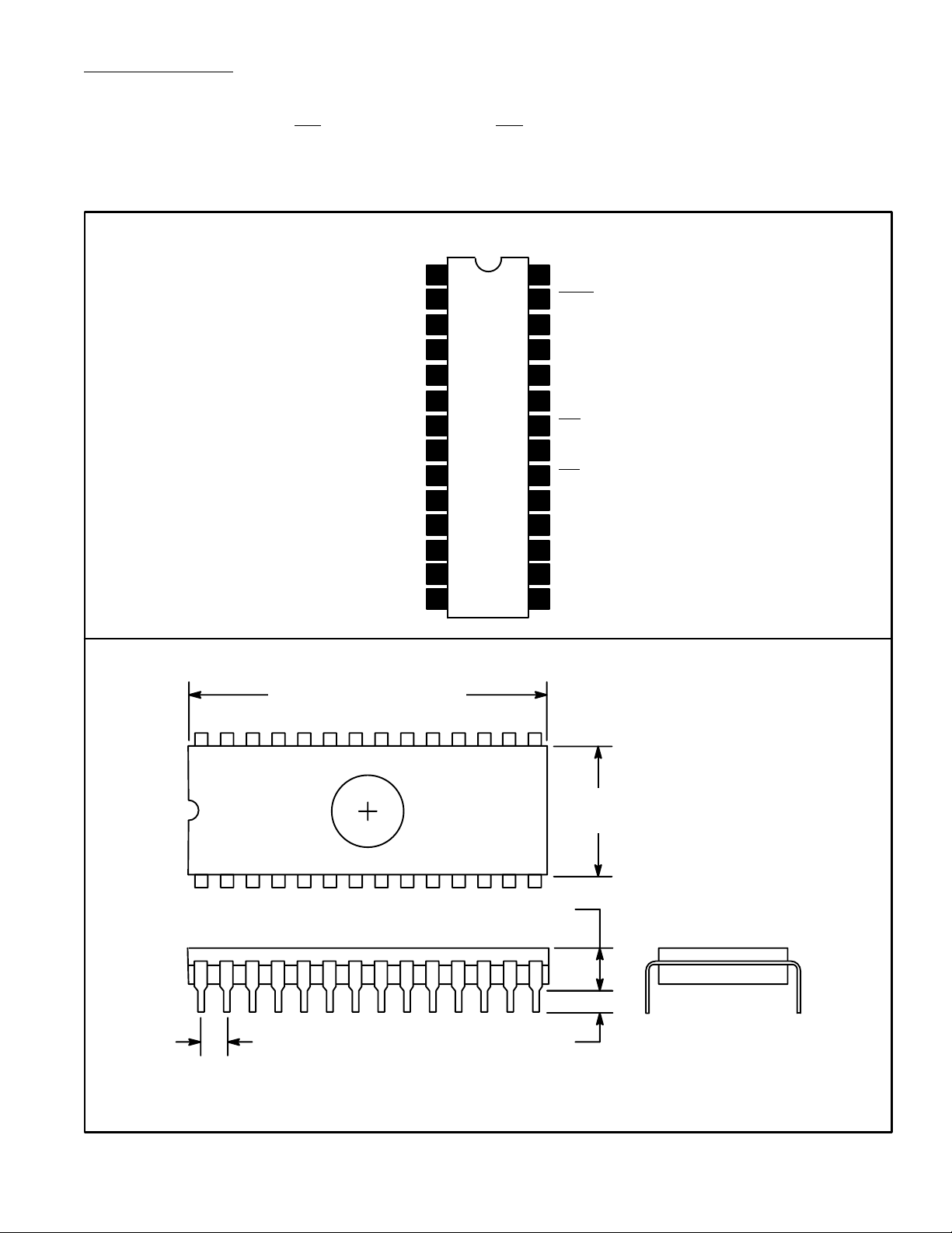
Pin Connection Diagram
V
PP
A12
A7
A6
A2
10A0
11
O0
O1
O2
14GND 15
1.480 (37.59) Max
1
2
3
4
5A5
6A4
7A3
8
9A1 20
28
27
26
25
24
23
22
21
19
18
16
V
CC
PGM
N.C.
A8
A9
A11
OE
A10
CE
O7
O6
O512 17
O413
O3
28 15
.580
(14.7)
114
.216 (5.5) Max
.100 (2.54) .100 (2.54) Min
 Loading...