

Page 1
NTE1932
Integrated Circuit
3–Terminal Positive Voltage Regulator,
10V, 1A
The NTE1932 fixed–voltage regulator is a monolithic integrated circuit in a TO220 type package designed for use in a wide variety of applications including local, on–card regulation. This regulator employs internal current limiting, thermal shutdown, and safe–area compensation. With adequate heatsinking it can deliver output currents in excess of 1.0 ampere. Although designed primarily as a fixed
voltage regulator, this device can be used with external components to obtain adjustable voltages and
currents.
Features:
D Thermal Overload Protection
D Internal Short–Circuit Current Limiting
D Output Transistor Safe–Area Compensation
Absolute Maximum Ratings:
Input Voltage, V
Power Dissipation (T
Power Dissipation (T
Operating Junction Temperature Range, T
Storage Junction Temperature Range, T
in
= +25°C), P
A
= +25°C), P
C
D
D
J
stg
Thermal Resistance, Junction–to–Ambient, R
Thermal Resistance, Junction–to–Case, R
thJC
0° to +150°C. . . . . . . . . . . . . . . . . . . . . . . . . . . . . . . . . . . .
–65° to +150°C. . . . . . . . . . . . . . . . . . . . . . . . . . . . . . . . . .
thJA
35V. . . . . . . . . . . . . . . . . . . . . . . . . . . . . . . . . . . . . . . . . . . . . . . . . . . . . . . . . . . . . . . . . . .
1.75W. . . . . . . . . . . . . . . . . . . . . . . . . . . . . . . . . . . . . . . . . . . . . . . .
20W. . . . . . . . . . . . . . . . . . . . . . . . . . . . . . . . . . . . . . . . . . . . . . . . .
65°C/W. . . . . . . . . . . . . . . . . . . . . . . . . . . . . . . . . . .
5°C/W. . . . . . . . . . . . . . . . . . . . . . . . . . . . . . . . . . . . . . .
Electrical Characteristics:
(Vin = 16V, IO = 500mA, CI = 0.33µF, CO = 0.1µF, TJ = 0° to +125°C
unless otherwise specified)
Parameter Symbol Test Conditions Min Typ Max Unit
Output Voltage V
Line Regulation Reg
Load Regulation Reg
TJ = +25°C 9.6 10.0 10.4 V
O
5mA ≤ IO ≤ 1A, PO ≤ 15W, 12.5V ≤ Vin ≤ 25V 9.5 10.0 10.5 V
lineTJ
loadTJ
= +25°C, Note 1 12.5V ≤ Vin ≤ 25V – 10 200 mV
13V ≤ Vin ≤ 20V – 3 100 mV
= +25°C, Note 1 5mA ≤ IO ≤ 1.5A – 12 200 mV
250mA ≤ IO ≤ 750mA – 4 100 mV
Note 1. Load and line regulation are specified at constant junction temperature. Changes in VO due
to heating effects must be taken into account separately. Pulse testing with low duty cycle
is used.
Page 2
Electrical Characteristics: (Vin = 16V, IO = 500mA, CI = 0.33µF, CO = 0.1µF, TJ = 0° to +125°C
unless otherwise specified)
Parameter Symbol Test Conditions Min Typ Max Unit
Quiescent Current I
Quiescent Current Change ∆I
TJ = +25°C – 4.3 8.0 mA
B
12.5V ≤ Vin ≤ 29V – – 1.0 mA
B
5mA ≤ IO ≤ 1A – – 0.5 mA
Ripple Rejection RR 14V ≤ Vin ≤ 23V, f = 120Hz 56 71 – dB
Dropout Voltage V
Output Noise Voltage V
Output Resistance r
Short–Circuit Current Limit I
Peak Output Current I
– VOTJ = +25°C, IO = 1A – 2 – V
in
TA = +25°C, 10Hz ≤ f ≤ 100kHz – 58 – µV/V
n
f = 1kHz – 17 – mΩ
O
sc
max
TA = +25°C, Vin = 35V – 420 – mA
TJ = +25°C – 2.2 – A
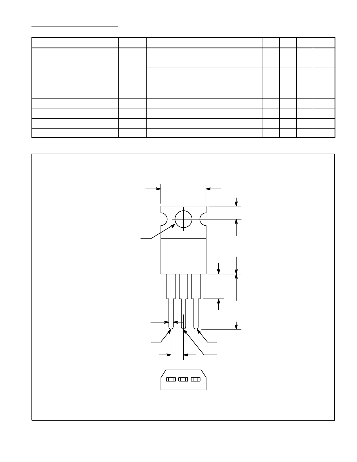
.420 (10.67)
Max
.110 (2.79)
O
.147 (3.75)
Dia Max
.070 (1.78)
Max
.100 (2.54)
.500
(12.7)
Max
.250 (6.35)
Max
.500
(12.7)
Min
V
IN
V
OUT
GND/Tab
 Loading...