

Page 1

NTE1854D/NTE1854M
Integrated Circuit
Dual Power Operational Amplifier
Description:
The NTE1854D/NTE1854M is a monolithic dual–power operational amplifier which features a high
current, low saturation voltage, flyback protected output stage optimized for driving heavy inductive
loads. Capable of operation in a single supply mode form as low as 4.5V up to 13.2V, the
NTE1854D/NTE1854M is ideally suited for the computer peripheral environment, driving small motors, solenoids, and linear actuators in an H–bridge configuration.
As a general–purpose op amp, the NTE1854D/NTE1854M exhibits low input offset voltage, high open
loop gain, low quiescent current, a large differential input voltage range, and a common–mode input
voltage range which includes ground (V
Features:
D Full output swing at ±500mA
D High inductive load drive capability
D Internal flyback protection diodes
D Low power dissipation
D Single or split supply operation
D Common–mode range includes ground (VEE)
D High open loop gain
D Low input offset voltage
D Large differential input voltage range
D Thermal shutdown protection
D Available in Two Package Types:
NTE1854M: 8–Lead Mini DIP
NTE1854D: 14–Lead DIP
EE
).
Absolute Maximum Ratings:
Supply Voltage (Single Supply), V
DC Output Current, I
OUT
Peak Output Current (Non–Repetitive), I
Common–Mode Input Voltage, V
Differential–Mode Input Voltage, V
Operational Junction Temperature, T
Storage Temperature Range, T
Lead Temperature (During Soldering, 10sec), T
(Note 1)
CC
ICM
IDM
J
stg
–0.3V to 14V. . . . . . . . . . . . . . . . . . . . . . . . . . . . . . . . . . . . . . . . . .
OUT
–0.3V to VCC –2V. . . . . . . . . . . . . . . . . . . . . . . . . . . . . . . . . . . . . .
. . . . . . . . . . . . . . . . . . . . . . . . . . . . . . . . . . . . . . . . . . . . . . . .
+150°C. . . . . . . . . . . . . . . . . . . . . . . . . . . . . . . . . . . . . . . . . . . . . .
–65°C to 150°C. . . . . . . . . . . . . . . . . . . . . . . . . . . . . . . . . . . . . . . . .
L
+300°C. . . . . . . . . . . . . . . . . . . . . . . . . . . . . . . . . . . .
±1.0A. . . . . . . . . . . . . . . . . . . . . . . . . . . . . . . . . . . . . . . . . . . . . . . . . . . . . . . . . .
±1.5A. . . . . . . . . . . . . . . . . . . . . . . . . . . . . . . . . . . . . . . . .
±V
CC
Note 1 Exceeding these ratings could cause damage to the device. All voltages are with respect
to GND. All currents are positive into the specified terminal.
Page 2
Recommended Operating Conditions:
Supply Voltage (Single Supply), V
DC Output Current, I
OUT
Common–mode Input Voltage, V
Differential–Mode Input Voltage, V
CC
ICM
IDM
. . . . . . . . . . . . . . . . . . . . . . . . . . . . . . . . . . . . . . . . . . . . . . . .
Operating Ambient Temperature Range, T
4.5V to 13.2V. . . . . . . . . . . . . . . . . . . . . . . . . . . . . . . . . . . . . . . . .
±500mA. . . . . . . . . . . . . . . . . . . . . . . . . . . . . . . . . . . . . . . . . . . . . . . . . . . . . . . .
0V to VCC –2V. . . . . . . . . . . . . . . . . . . . . . . . . . . . . . . . . . . . . . . .
±V
CC
A
0°C to 70°C. . . . . . . . . . . . . . . . . . . . . . . . . . . . . . . . . . . . .
Electrical Specifications:
(VCC = 12V, TA = 25°C, unless otherwise specified.)
Parameter Symbol Test Conditions Min Typ Max Unit
STATIC CHARACTERISTICS
Input Offset Voltage V
Input Bias Current I
Input Offset Current I
OS
Difference Input Resistance R
Source Side Output Saturation Voltage (+) V
Sink Side Output Saturation Voltage (–)V
Open Loop Voltage Gain A
VOL
IO
TA = T
B
TA = T
ID
SATIOUT
I
OUT
SATIOUT
I
OUT
to T
MIN
MIN
to T
MAX
MAX
= –100mA – 0.8 – V
= –500mA – 1.0 1.5 V
= –100mA – 0.3 – V
= –500mA – 0.6 1.0 V
–15 0 +15 mV
–30 – +30 mV
–1.0 –0.2 – µA
–50 – +50 nA
–200 – +200 nA
500 – – KΩ
70 90 – dB
Common–Mode Rejection Ratio CMRR 66 90 – dB
Power Supply Rejection Ratio PSRR 60 80 – dB
Quiescent Drain Current I
CC
– 7 15 mA
Thermal Shutdown Temperature – 175 – °C
DYNAMIC CHARACTERISTICS
Gain Bandwidth Product GBWP RL = ∞Ω – 800 – kHz
Slew Rate dVO/dt AV = 1 – 1.6 – V/µs
Power Bandwidth, –3dB PBW – 200 – kHz
Input Noise Voltage E
Input Noise Current I
Channel Separation C
22Hz to 22kHz – 10 – µV
N
22Hz to 22kHz – 200 – pA
N
f = 1kHz, RL = 10Ω,
S
AV
= 30dB
CL
– 60 – dB
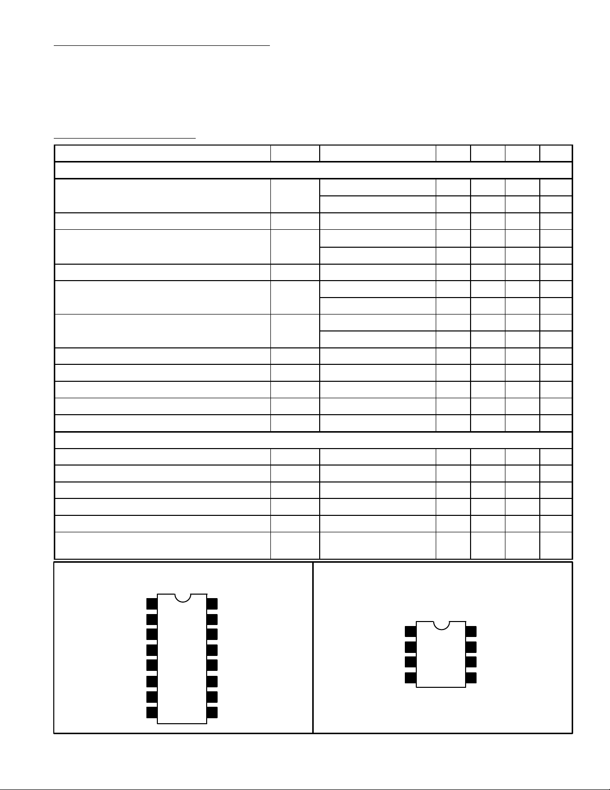
Pin Connection Diagram
Supply Voltage
Output 2
GND
NTE1854D
1
2
3
4
5Inverted Input 2
6Non–Inverted Input 2
7Non–Inverted Input 1
8Inverted Input 1 9 GND
GNDOutput 1
16
15
GND
14
GND
13
GND
12 GND
11 GND
10 GND
Pin Connection Diagram
Output 1
Supply Voltage
Output 2
GND
NTE1854M
1
2
3
4
Inverted Input 1
8
Non–Inverted Input 1
7
Non–Inverted Input 2
6
Inverted Input 2
5
Page 3

16 9
.260 (6.6) Max
18
.245
(6.22)
Min
.785 (19.9)
Max
.100 (2.54)
.700 (17.7)
85
.260 (6.6)
.300
(7.62)
.200 (5.08)
Max
.100 (2.54)
14
.390 (9.9)
Max
.155
(3.93)
.300 (7.62)
.300
(7.62)
.145 (3.68)
 Loading...