

Page 1

NTE1851
Integrated Circuit
Audio Amplifier, 24W BTL
Description:
The NTE1851 is a monolithic integrated class–B amplifier in a 13–Lead Staggered SIP type package
primarily developed for car radio applications, and also to drive low–impedance loads (down to 1.6Ω).
At a supply voltage V
Load), or, when used as a stereo amplifier, it delivers 2 x 11W into 2Ω or 2 x 6.5W into 4Ω.
Features:
D Flexibility In Use – Mono BTL as well as Stereo
D High Output Power
D Low Offset Voltage at the Output
(Important for BTL)
D Large Usable Gain Variation
D Very Good Ripple Rejection
D Internal Limited Bandwidth f or High Frequencies
D Low Standby Current Possiblity (1µA Typ), to
Simplify Required Switches: TTL Drive Possible
D Low Number of Small–Sized External Compo -
nents
= 14.4V, an output power of 21W can be delivered into a 4Ω BTL (Bridge–Tied
CC
D High Reliability
D Load Dump Protection
D AC and DC Short–Circuit Safe to Ground up to
= 18V
V
CC
D Thermal Protection
D Speaker Protection in Bridge Configuration
D SOAR Protection
D Outputs Short–Circuit Safe to Ground in BTL
D Reverse–Polarity Safe
Applications:
D Car Radio Applications
D Drive Low Impedance Loads
D Stereo Amplifier
Absolute Maximum Ratings:
Supply Voltage (Pin10), V
CC
Operating 18V. . . . . . . . . . . . . . . . . . . . . . . . . . . . . . . . . . . . . . . . . . . . . . . . . . . . . . . . . . . . . . . . . . .
Non–Operating 28V. . . . . . . . . . . . . . . . . . . . . . . . . . . . . . . . . . . . . . . . . . . . . . . . . . . . . . . . . . . . . .
Supply Voltage (During 50ms Load Dump Protection), V
Peak Output Current, I
Crystal Temperature, T
Storage Temperature Range, T
OM
C
stg
CC
+150°C. . . . . . . . . . . . . . . . . . . . . . . . . . . . . . . . . . . . . . . . . . . . . . . . . . . . . . . . .
–65° to +150°C. . . . . . . . . . . . . . . . . . . . . . . . . . . . . . . . . . . . . . . . . .
AC and DC Short–Circuit Safe Voltage 18V. . . . . . . . . . . . . . . . . . . . . . . . . . . . . . . . . . . . . . . . . . . . . . . .
Reverse Polarity 10V. . . . . . . . . . . . . . . . . . . . . . . . . . . . . . . . . . . . . . . . . . . . . . . . . . . . . . . . . . . . . . . . . . .
45V. . . . . . . . . . . . . . . . . . . . . . . . . . . . . .
8A. . . . . . . . . . . . . . . . . . . . . . . . . . . . . . . . . . . . . . . . . . . . . . . . . . . . . . . . . . . .
Page 2
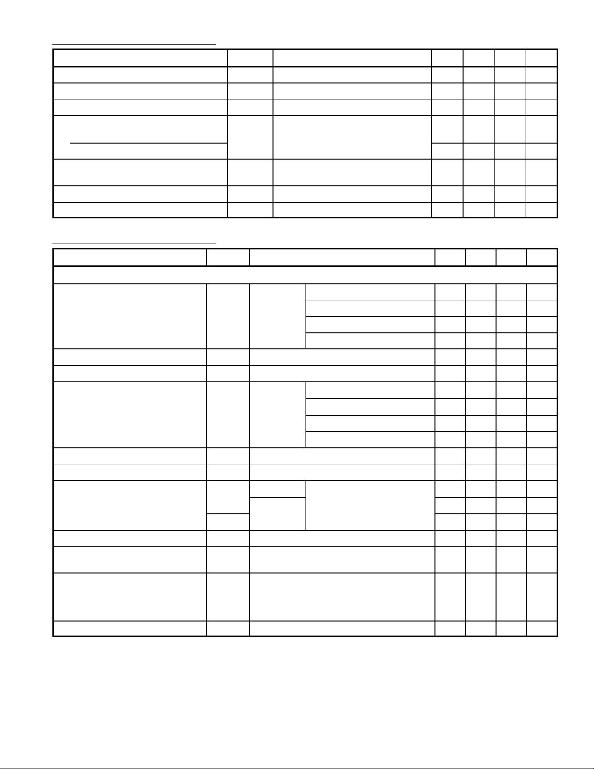
DC Electrical Characteristics:
Parameter Symbol Test Conditions Min Typ Max Unit
Supply Voltage Range (Pin10) V
Repetitive Peak Output Current I
Total Quiescent Current I
Switching Level 11
OFF
CC
ORM
TOT
V
11
6 – 18 V
– – 4 A
– 75 75 mA
V
– – 1.8
ON 3.0 – – V
Impedance Between Pin10 & Pin6;
|Z
| Standby Position V11 < 1.8V 100 – –
OFF
kΩ
Pin10 & Pin8
Standby Current I
Switch–On Current (Pin11) I
SB
SO
V11 = 0 to 0.8V – 1 100 µA
V11 ≤ V
10
– 10 100 µA
AC Electrical Characteristics: (TA = +25°C, VCC = 14.4V, f = 1kHz unless otherwise specified)
Parameter Symbol Test Conditions Min Typ Max Unit
Bridge–Tied Load Application (BTL)
Output Power with Bootstrap P
Open–Loop Voltage Gain G
Closed–Loop Voltage Gain G
Output Power without Bootstrap
P
RL = 4Ω
O
O
Note 2 – 40 – dB
C
Note 3 VCC = 14.4V, d
O
Frequency Response at –3dB B Note 4 20 – 20 Hz
Input Impedance |Zi| Note 5 1 – –
Noise Input Voltage (RMS Value)
V
N(RMS)
RS = 0Ω
RS = 10kΩ – 0.35 0.35 mV
VCC = 14.4V, d
VCC = 14.4V, d
VCC = 13.2V, d
VCC = 13.2V, d
= 0.5% 15.5 18.0 – W
TOT
= 10% 20 24 – W
TOT
= 0.5% – 15 – W
TOT
= 10% – 20 – W
TOT
– 75 – dB
= 0.5% – 12 12 W
TOT
VCC = 14.4V, d
VCC = 13.2V, d
VCC = 13.2V, d
= 10% – 15 15 W
TOT
= 0.5% – 9 9 W
TOT
= 10% – 12 12 W
TOT
MΩ
f = 20Hz to 20kHz – 0.2 0.2 mV
V
N
– 0.25 0.8 mV
Supply Voltage Ripple Rejection RR f = 100Hz 42 50 50 dB
DC Output Offset Voltage
|∆V
| – 2 50 mV
5–9
Between the Outputs
Loudspeaker Protection
|∆V
| – – 1 V
5–9
(All Conditions)
Maximum DC Voltage
(Across the Load)
Power Bandwidth B –1dB, d
= 0.5% 30 – 40 kHz
TOT
Note 1. The internal circuit impedance at Pin11 is > 5kΩ if V11 > V10.
Note 2. Closed–Loop voltage gain can be chosen between 32 and 56dB (BTL), and is determined
by external components.
Note 3. Without the bootstrap the 100µF capacitor between Pin5 and Pin6 (Pin8 and Pin9) can be
omitted. Pin6, Pin8, and Pin10 have to be interconnected.
Note 4. Frequency response externally fixed.
Note 5. The input impedance in the test circuit is typically 100kΩ.
Page 3

AC Electrical Characteristics (Cont’d): (TA = +25°C, VCC = 14.4V, f = 1kHz unless otherwise
specified)
Parameter Symbol Test Conditions Min Typ Max Unit
Stereo Application
Output Power with Bootstrap P
Output Power with Bootstrap P
Output Power without Bootstrap P
Frequency Response at –3dB B Note 4 40 – 20 kHz
Supply Voltage Ripple Rejection RR Note 8 – 50 – dB
Channel Separation α RS = 10kΩ, f = 1kHz 40 50 – dB
Closed–Loop Voltage Gain G
Noise Input Voltage (RMS Value)
V
N(RMS)
V
d
O
O
O
C
N
= 10%
TOT
Note 6
d
= 0.5%
TOT
Note 6
d
= 10%, VCC = 14.4V, RL = 4Ω,
TOT
Note 3, Note 6, & Note 7
Note 9 – 40 – dB
RS = 0Ω
RS = 10kΩ – 0.25 – mV
VCC = 14.4V, RL = 4Ω 6 7 – W
VCC = 14.4V, RL = 2Ω 10 12 – W
VCC = 13.2V, RL = 4Ω – 6 – W
VCC = 13.2V, RL = 4Ω – 10 – W
VCC = 14.4V, RL = 4Ω – 5.5 – W
VCC = 14.4V, RL = 2Ω – 9.0 – W
VCC = 13.2V, RL = 4Ω – 4.5 – W
VCC = 13.2V, RL = 4Ω – 7.5 – W
– 6 – W
f = 20Hz to 20kHz – 0.15 – mV
– 0.2 – mV
Note 1. The internal circuit impedance at Pin11 is > 5kΩ if V11 > V10.
Note 2. Closed–Loop voltage gain can be chosen between 32 and 56dB (BTL), and is determined
by external components.
Note 3. Without the bootstrap the 100µF capacitor between Pin5 and Pin6 (Pin8 and Pin9) can be
omitted. Pin6, Pin8, and Pin10 have to be interconnected.
Note 4. Frequency response externally fixed.
Note 5. The input impedance in the test circuit is typically 100kΩ.
Note 6. Output power is measured directly at the output pins of the IC.
Note 7. A resistor of 56kΩ between Pin3 and Pin7 to reach symmetrical clipping.
Note 8. Supply voltage ripple rejection measured with a source impedance of 0Ω (Maximum ripple
amplitude: 2V).
Note 9. Closed–Loop voltage gain can be chosen between 26 and 50dB (Stereo), and is determined
by external components.
Page 4

Pin Connection Diagram
(Front View)
Inverting Input 213
12 Non–Inverting Input 2
Standby Switching
11
10
V
CC
9
Output 2
8
Bootstrap 2
7
GND/Substrate
6
Bootstrap 1
5
Output 1
4
Loudspeaker Protection
Supply Voltage
3
Ripple Rejection
2
Non–Inverting Input 1
Inverting Input 1
1
.961 (24.4) .185 (4.7)
.488
.128
(3.28)
113
(12.4)
.630
(16.0)
.669
(17.0)
.170 (4.32).067 (1.7) .200 (5.08)
 Loading...