

Page 1

NTE1786
Integrated Circuit
Frequency Lock Loop (FLL)
Tuning & Control Circuit
Description:
The NTE1786 is an integrated circuit in a 24–Lead DIP type package that provides closed–loop digital
tuning of TV receivers, with or without AFC, as required. This device also controls up to 4 analog functions, 4 general purpose I/O ports and 4 high–current outputs for tuner band selection.
Features:
D Combined Analog and Digital Circuitry Minimizes the Number of Additional Interfacing Components
Required
D Frequency Measurement with Resolution of 50kHz
D Selectable Prescaler Divisor of 64 or 256
D 32V Tuning Voltage Amplifier
D 4 High–Current Outputs for Direct Band Selection
D 4 Static Digital–to–Analog Convertors (DACs) for Control of Analog Functions
D 4 General Purpose Input/Output (I/O) Ports
D Tuning with Control of Speed and Direction
D Tuning with or without AFC
D Single–Pin, 4MHz On–Chip Oscillator
2
D I
C Bus Slave Transceiver
Applications:
D TV Receivers
D Satellite Receivers
D CATV Converters
Absolute Maximum Ratings:
Supply Voltage Ranges,
Pin13, V
Pin19, V
Pin14, V
CC1
CC2
CC3
–0.3 to +18V. . . . . . . . . . . . . . . . . . . . . . . . . . . . . . . . . . . . . . . . . . . . . . . . . . . . . . . . .
–0.3 to +18V. . . . . . . . . . . . . . . . . . . . . . . . . . . . . . . . . . . . . . . . . . . . . . . . . . . . . . . . .
–0.3 to +36V. . . . . . . . . . . . . . . . . . . . . . . . . . . . . . . . . . . . . . . . . . . . . . . . . . . . . . . . .
Page 2
Absolute Maximum Ratings (Cont’d):
Input/Output Voltage Ranges,
Pin2, V
Pin3, V
Pin4 to Pin7, V
Pin8 & Pin9 (Note 1), V
Pin10, V
Pin12 (Note 2), V
Pin15 to Pin18 (Note 2), V
Pin20 (Note 1), V
Pin21, V
Pin1, Pin22 to Pin24 (Note 1), V
Total Power Dissipation, P
Operating Ambient Temperature Range, T
Storage Temperature Range, T
SDA
SCL
P2X
, V
AFC+
. . . . . . . . . . . . . . . . . . . . . . . . . . . . . . . . . . . . . . . . . . . . . . . . . . . . . . . . . . .
TI
. . . . . . . . . . . . . . . . . . . . . . . . . . . . . . . . . . . . . . . . . . . . . . . . .
TUN
. . . . . . . . . . . . . . . . . . . . . . . . . . . . . . . . . . . . . . . . . . . . . . . . .
FDIV
OSC
TOT
stg
AFC–
. . . . . . . . . . . . . . . . . . . . . . . . . . . . . . . . . . . . . . . . . .
P1X
. . . . . . . . . . . . . . . . . . . . . . . . . . . . . . . . . . . . .
DACX
. . . . . . . . . . . . . . . . . . . . . . . . . . . . . . . . . . .
A
Note 1. Pin voltage may exceed supply voltage if current is limited to 10mA.
Note 2. Pin voltage must not exceed 18v but may exceed V
DC and AC Electrical Characteristics:
(TA = +25°C, V
CC1
of current is limited to 200mA.
CC2
, V
CC2
, V
at typical voltages
CC3
unless otherwise specified)
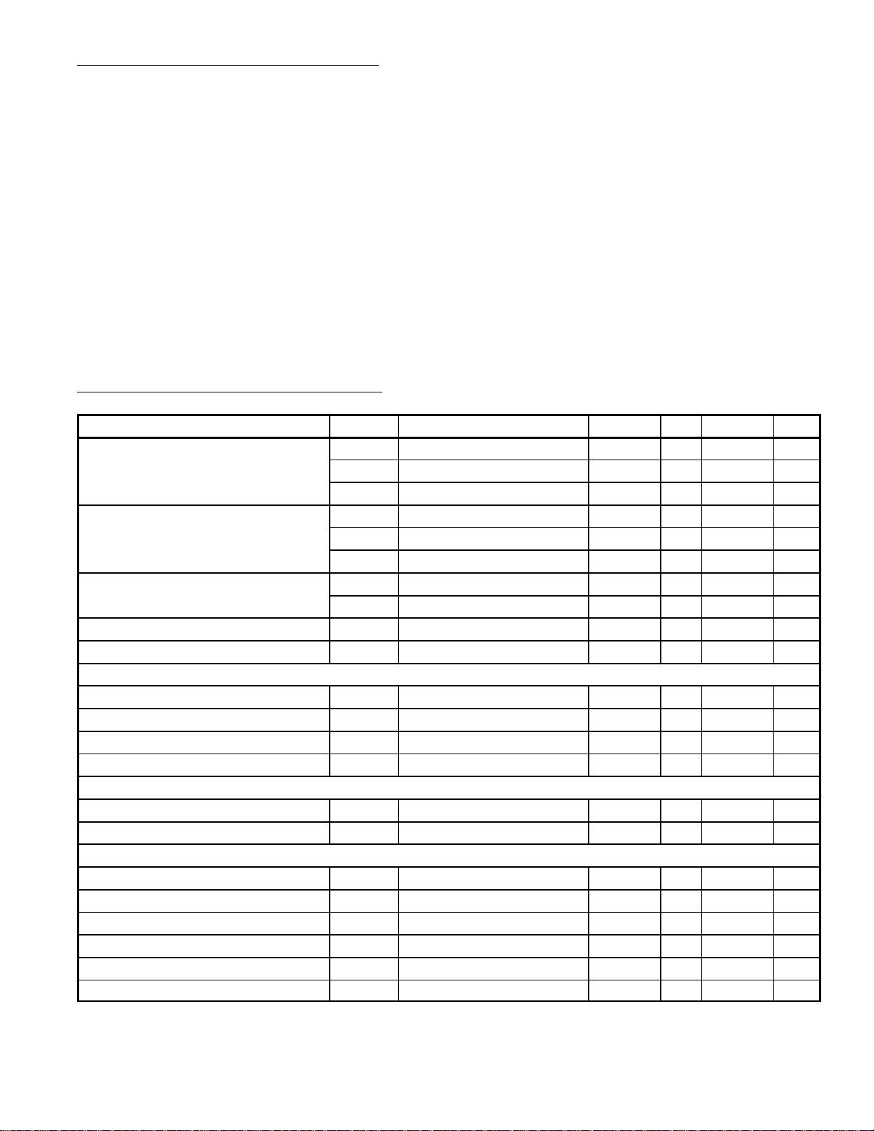
Parameter Symbol Test Conditions Min Typ Max Unit
Supply Voltage V
Supply Current (No Outputs Loaded) I
Additional Supply Currents (A) I
Total Power Dissipation P
Operating Ambient Temperature T
I2C Bus Inuts SDA Input (Pin2); SCL Input (Pin3)
Input Voltage, HIGH V
Input Voltage, LOW V
Input Current, HIGH I
Input Current, LOW I
I2C Bus Outputs SDA Output (Pin2, Open Collector)
Output Voltage, LOW V
Maximum Output Sink Current I
Open–Collector I/O Ports P20, P21, P22, P23 (Pin4 to Pin7, Open Collector)
Input Voltage, HIGH V
Input Voltage, LOW V
Input Current, HIGH I
Input Current, LOW I
Output Voltage, LOW V
Maximum Output Sink Current I
CC1
V
CC2
V
CC3
CC1
I
CC2
I
CC3
CC2A
I
CC3A
TOT
IH
IL
OL
OL
IH
IL
OL
OL
Note 3 –2 – I
Note 3 0.2 – 2.0 mA
A
Note 4 3 – VCC–1 V
IH
IL
Note 4 – – 10 µA
IOL = 3mA – – 0.4 V
IH
IL
IOL = 2mA – – 0.4 V
10.5 12.0 13.5 V
4.7 13.0 16.0 V
30 32 35 V
18 30 45 mA
0 – 0.1 mA
0.2 0.6 2.0 mA
– 380 – mW
–20 – +70 °C
–0.3 – 1.5 V
– – 10 µA
– 5 – mA
2 – 16 V
–0.3 – 0.8 V
– – 25 µA
– – 25 µA
– 4 – mA
–0.3 to +18V. . . . . . . . . . . . . . . . . . . . . . . . . . . . . . . . . . . . . . . . . . . . . . . . . . . . . . . . . .
–0.3 to +18V. . . . . . . . . . . . . . . . . . . . . . . . . . . . . . . . . . . . . . . . . . . . . . . . . . . . . . . . . .
–0.3 to +18V. . . . . . . . . . . . . . . . . . . . . . . . . . . . . . . . . . . . . . . . . . . . . . . . . . . .
–0.3 to V
–0.3 to V
–0.3 to V
–0.3 to V
–0.3 to V
–0.3 to +5V. . . . . . . . . . . . . . . . . . . . . . . . . . . . . . . . . . . . . . . . . . . . . . . . . . . . . . . . . .
–0.3 to V
–20° to +70°C. . . . . . . . . . . . . . . . . . . . . . . . . . . . . . . . . . .
–65° to +150°C. . . . . . . . . . . . . . . . . . . . . . . . . . . . . . . . . . . . . . . . . .
OHP1X
CC1
CC1
CC3
CC2
CC1
CC1
1000mW. . . . . . . . . . . . . . . . . . . . . . . . . . . . . . . . . . . . . . . . . . . . . . . . . . .
mA
Note 3. For each band–select output which is programmed at logic 1, sourcing a current I
additional supply currents (A) shown must be added to I
Note 4. If V
< 1V, the input current is limited to 10µA at input voltages up to 16V.
CC1
CC2
and I
, respectively.
CC3
OOP1X
, the
Page 3

DC and AC Electrical Characteristics (Cont’d): (TA = +25°C, V
CC1
, V
CC2
, V
at typical voltages
CC3
unless otherwise specified)
Parameter Symbol Test Conditions Min Typ Max Unit
AFC Amplifier Inputs AFC+, AFC– (Pin8, Pin9)
Transconductance for Input Voltages
up to 1V Differential
g00 AFCS1: 0, AFCS2: 0 100 250 800 nA/V
g01 AFCS1: 0, AFCS2: 1 15 25 35 µA/V
g10 AFCS1: 1, AFCS2: 0 30 50 70 µA/V
g1 1 AFCS1: 1, AFCS2: 1 60 100 140 µA/V
Tolerance of Transconductance
∆M
g
–20 – +20 %
Multiplying Factor (2, 4, or 8)
when Correction–in–Band is
Used
Input Offset Voltage V
Common–Mode Input Voltage V
IOFF
COM
–75 – +75 mV
3 – V
–2.5 V
CC1
Common–Mode Rejection Ratio CMRR – 50 – dB
Power Supply (V
Input Current I
) Rejection Ratio PSRR – 50 – dB
CC1
I
– – 500 nA
Tuning Voltage Amplifier Input TI, Output TUN (Pin10, Pin12)
Maximum Output Voltage V
Maximum Output Voltage V
TUNILOAD
TM00ILOAD
= ±2.5mA V
= ±2.5mA, VTMI1: 0,
–1.6 – V
CC3
–0.4 V
CC3
300 – 500 mV
VTMI0: 0
V
TM10ILOAD
= ±2.5mA, VTMI1: 1,
450 – 650 mV
VTMI0: 0
V
TM11ILOAD
= ±2.5mA, VTMI1: 1,
650 – 900 mV
VTMI0: 1
Maximum Output Source Current –I
Maximum Output Sink Current I
Input Bias Current I
Power Supply (V
Minimum Charge IT to Tuning
Voltage Amplifier
) Rejection Ratio PSRR – 60 – dB
CC3
CH
CH
CH
CH
Tolerance of Charge (or ∆V
TUN
)
TUNH
TUNL
TI
TUHN1: 0, TUHN0: 0 0.4 1.0 1.7 µA/V
00
TUHN1: 0, TUHN0: 1 4 8 14 µA/V
01
TUHN1: 1, TUHN0: 0 15 30 48 µA/V
10
TUHN1: 1, TUHN0: 1 130 250 370 µA/V
11
∆CH –20 – +20 %
2.5 – 8.0 mA
– 40 – mA
–5 – +5 nA
Multiplying Factor when COIB
and/or TUS are Used
Maximum Current I into Tuning
Amplifier
I
T00
I
T01
I
T10
I
T11
TUHN1: 0, TUHN0: 0 1.7 3.5 5.1 µA
TUHN1: 0, TUHN0: 1 15 29 41 µA
TUHN1: 1, TUHN0: 0 65 110 160 µA
TUHN1: 1, TUHN0: 1 530 875 1220 µA
Correction–in–Band
Tolerance of Correction–in–Band
∆V
CIB
–15 – +15 %
Levels 12V, 18V, and 24V
Band–Select Output Ports P10, P11, P12, P13 (Pin15 to Pin18)
Output Voltge, HIGH V
Output Voltage, LOW V
OH
OL
–IOH = 50mA, Note 5 V
–0.6 – – V
CC2
IOL = 2mA – – 0.4 V
Note 5. At continuous operation the output current should not exceed 50mA. When the output is
short–circuited to GND for several seconds the device may be damaged.
Page 4

DC and AC Electrical Characteristics (Cont’d): (TA = +25°C, V
CC1
, V
CC2
, V
at typical voltages
CC3
unless otherwise specified)
Parameter Symbol Test Conditions Min Typ Max Unit
Band–Select Output Ports (Cont’d) P10, P11, P12, P13 (Pin15 to Pin18)
Maximum Output Source Current –I
Maximum Output Sink Current I
OH
OL
FDIV Input (Pin20)
Input Voltage (Peak–to–Peak Value) V
FDIV
Duty Cycle 40 – 60 %
Maximum Input Frequency f
MAX
Input Impedance Z
Input Capacitance C
OSC Input (Pin21)
Crystal Resistance at Resonance
R
(4MHz)
DAC Outputs (Pin1, Pin22 to Pin24)
Maximum Output Voltage (No Load) V
Minimum Output Voltage (No Load) V
DH
DL
Positive Value of Smallest Step ∆V
Deviation from Linearity – – 0.5 V
Output Impedance Z
Maximum Output Source Current –I
Maximum Output Sink Current I
DH
DL
Power–Down Reset
Maximum Supply Voltage (V
CC1
) at
V
PD
which Power–Down Reset is
Active
V
Rise Time During Power–Up
CC1
(Up to V
PD
)
t
Voltage Level for Valid Module Address
Voltage Level at P20 (Pin4) for Valid
Module Address as a Function of
MA1, MA0
MA1, MA0
V
V
V
V
VA00
VA01
VA10
VA11
Note 5 – 130 200 mA
– 5 – mA
P–P)
t
RISE
and t
≤ 40ns 0.1 – 2.0 V
FALL
14.5 – – MHz
i
I
X
V
= 12V, Note 6 10.0 – 11.5 V
CC1
V
= 12V, Note 6 0.1 – 1.0 V
CC1
1 Least Significant Bit 0 – 350 mV
D
I
D
= ±2mA – – 70 Ω
LOAD
– 8 – kΩ
– 5 – pF
– – 150 Ω
– – 6 mA
– 8 – mA
7.5 – 9.5 V
R
5 – – µs
MA1: 0, MA0: 0 –0.3 – 16 V
MA1: 0, MA0: 1 –0.3 – 0.8 V
MA1: 1, MA0: 0 2.5 – V
MA1: 1, MA0: 1 V
–0.3 – V
CC1
–2 V
CC1
CC1
V
Note 5. At continuous operation the output current should not exceed 50mA. When the output is
short–circuited to GND for several seconds the device may be damaged.
Note 6. Values are proportional to V
CC1
.
Page 5

Pin Connection Diagram
DAC3 Output
Serial Data Line
Serial Clock Line
P20
I/O Ports
P23
AFC (–) Input
Tuning Voltage Amp
Invert Input
Tuning Voltage Amp
Output
1
2
3
4
5P21
6P22
7
8AFC (+) Input
9
10
11GND
24
23
22
21
20
19
18
17
16
15
14
12 13
DAC2 Output
DAC1 Output
DAC0 Output
X’tal OSC Input
Prescaler Input
2 (13V Typ)
V
CC
P13
P12
Band Select
Output Ports
P11
P10
3 (32V Typ)
V
CC
VCC 1 (12V Typ)
24 13
112
1.300 (33.02)
Max
.520
(13.2)
.255
(5.73)
Max
.100 (2.54)
.126
1.100 (27.94)
(3.22)
Min
.600
(15.24)
 Loading...