

Page 1
NTE1784
Integrated Circuit
TV Horizontal Processor
Description:
The NTE1784 is an integrated circuit in a 16–Lead DIP type package designed for use as a horizontal
processor circuit for B/W and color television receivers.
Features:
D Noise Gated Horizontal Sync Separator
D Noise Gated Vertical Sync Separator
D Horizonyal Oscillator with Frequency Range Limiter
D Phase Comparator between Sync Pulses and Oscillator Pulses (PLL)
D Phase Comparator between Flyback Pulses and Oscillator Pulses (PLL)
D Loop Gain and Time Constant Switching (VCR)
D Composite Blanking and Key Pulse Generator
D Protection Circuits
D Output Stages with High Current Capability
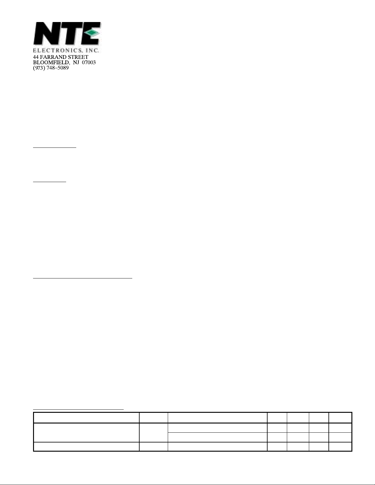
Absolute Maximum Ratings:
Supply Voltage (Pin1), V
Circuit Voltage, V
Circuit Voltage, V
Circuit Voltage, V
Circuit Voltage, V
2
4
8
9
, V
Peak Circuit Current, I
Peak Circuit Current, I
Circuit Current, I
Circuit Current, I
, I
6
7
S
. . . . . . . . . . . . . . . . . . . . . . . . . . . . . . . . . . . . . . . . . . . . . . . . . . . . . . . . . . . . . . .
11
2
3
10
Total Power Dissipation (T
Operating Junction Temperature Range, T
Storage Temperature Range, T
(TA = +25°C unless otherwise specified)
≤ +70°C), P
A
stg
tot
J
Maximum Thermal Resistance, Junction–to–Ambient, R
Electrical Characteristics:
Parameter Symbol Test Conditions Min Typ Max Unit
Supply Voltage V
Supply Current I
(TA = +25°C, VS = 12V unless otherwise specified)
S
Output pulses at Pin2 and Pin3 OFF – – 4 V
I3 = 0 – 40 52 mA
S
thJA
VS to –6V. . . . . . . . . . . . . . . . . . . . . . . . . . . . . . . . . . . . . . . . . . . . . . . . . . . . . . . . . . . . .
+6V to –6V. . . . . . . . . . . . . . . . . . . . . . . . . . . . . . . . . . . . . . . . . . . . . . . . . . . . . . . . . . .
500mA. . . . . . . . . . . . . . . . . . . . . . . . . . . . . . . . . . . . . . . . . . . . . . . . . . . . . . . . . .
30mA. . . . . . . . . . . . . . . . . . . . . . . . . . . . . . . . . . . . . . . . . . . . . . . . . . . . . . . . . . . . .
20mA. . . . . . . . . . . . . . . . . . . . . . . . . . . . . . . . . . . . . . . . . . . . . . . . . . . . . . . . . . . . . . . . .
–40° to +150°C. . . . . . . . . . . . . . . . . . . . . . . . . . . . . . . . . .
–40° to +150°C. . . . . . . . . . . . . . . . . . . . . . . . . . . . . . . . . . . . . . . . . .
80°C/W. . . . . . . . . . . . . . . . . . . . . . . . .
10.0 12.0 13.2 V
15V. . . . . . . . . . . . . . . . . . . . . . . . . . . . . . . . . . . . . . . . . . . . . . . . . . . . . . . . . . .
18V. . . . . . . . . . . . . . . . . . . . . . . . . . . . . . . . . . . . . . . . . . . . . . . . . . . . . . . . . . . . . . . . . .
V
S
1A. . . . . . . . . . . . . . . . . . . . . . . . . . . . . . . . . . . . . . . . . . . . . . . . . . . . . . . . . . . . . .
1W. . . . . . . . . . . . . . . . . . . . . . . . . . . . . . . . . . . . . . . . . . . . .
Page 2
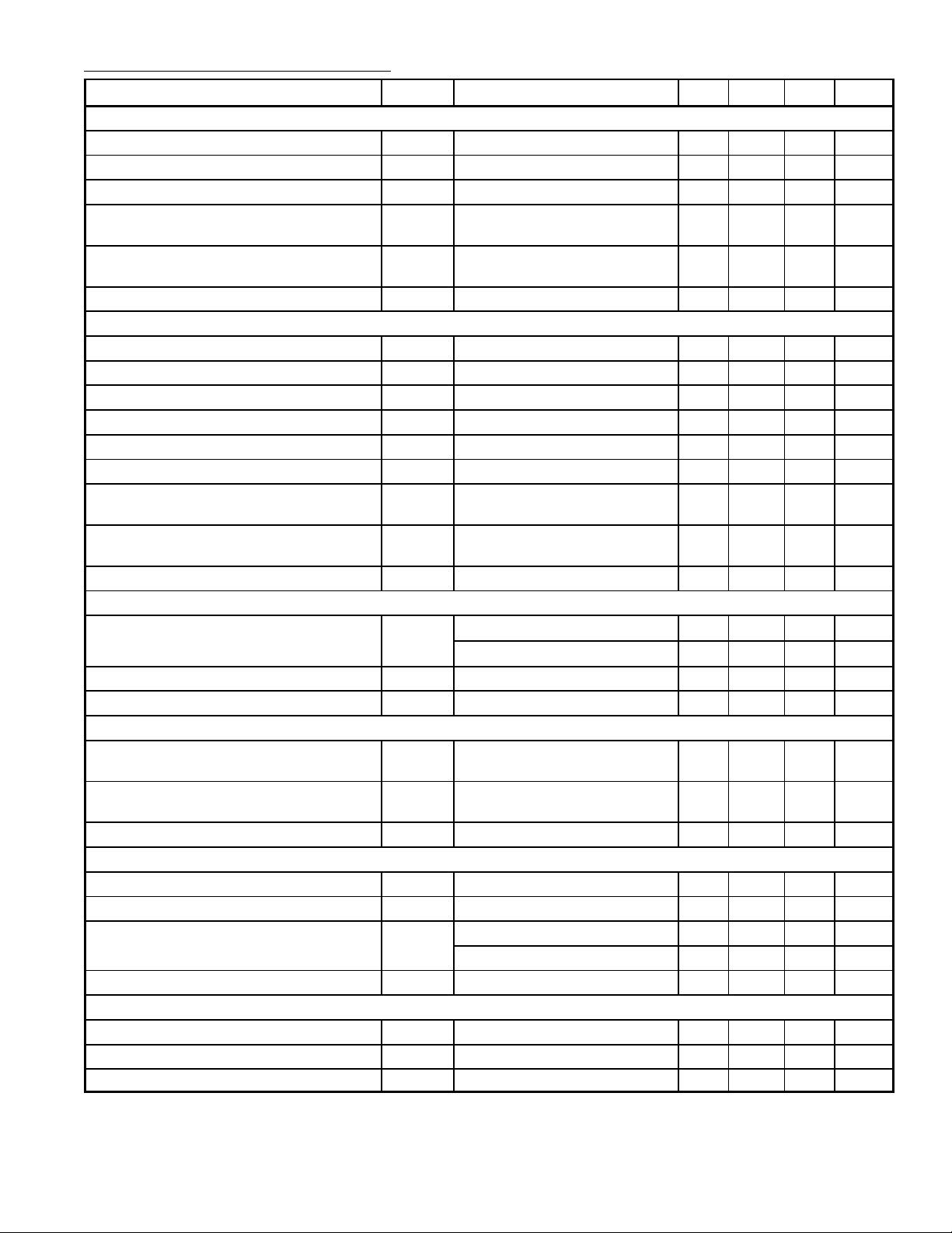
Electrical Characteristics (Cont’d): (TA = +25°C, VS = 12V unless otherwise specified)
Parameter Symbol Test Conditions Min Typ Max Unit
Horizontal Sync Separator and Noise Gate
Input Signal (Peak–to–Peak) V
Input Switching Voltage V
Input Switching Current I
Input Blocking Current for Noise
Suppression
Input Switching Voltage for Noise
V
Suppression
Leakage Current I
Vertical Sync Separator
Input Signal (Peak–to–Peak) V
Input Switching Voltage V
Input Switching Current I
Leakage Current I
Vertical Sync Pulse Output Voltage V
Output Resistance R
Delay between Leading Edge of Input
t
and Output Signals
Delay between Trailing Edge of Input
t
and Output Signals
Vertical Sync Pulse Duration t
Protection Circuit
Input Voltage for Switching Off the
V
Output Pulses
Input Resistance R
Input Current I
Flyback Pulse
Input Threshold Voltage of Blanking
V
‘Generator
Input Threshold Voltage of Phase
V
Comparator
Input Switching Current I
Output Pulse
Output Voltage (Peak–to–Peak) V
Output Current I
Output Resistance R
Output Pulse Duration t
Composite Blanking and Key Pulse
Key Pulse Output Peak Voltage V
Blanking Pulse Output Voltage V
Output Resistance R
I
LV
TV
7K
7B
i
I8 = 80µA – 1.5 – V
8
V8 = 1.4V – 10 – µA
8
8
8
V8 = –5V – – 1 µA
8
i
I9 = 80µA – 1.5 – V
9
I9 = 1.4V – 5 – µA
9
V9 = –5V – – 1 µA
9
No load at Pin10 11 – – kΩ
10
10
V
Output pulses OFF – – 0.5 V
4
Output pulses ON 1 – – V
4
4
6
6
V6 ≥ 1.7V – 0.23 – mA
6
I3 = 150mA
3
V3 = 5V – 500 – mA
3
At leading edge of output pulse – 3 – Ω
3
P–P
At trailing edge of output pulses – 20 – Ω
p
7
1 3 6 V
– 0.9 – mA
– 2.1 – V
1 3 6 V
– 10 – kΩ
– 17 – µs
– 50 – µs
– 190 – µs
– 200 – kΩ
5 – – µA
– 1.5 – V
– 7.6 – V
– 10 – V
20 22 26 µs
9 11 – V
4.2 4.5 4.8 V
– 100 – Ω
Page 3

Electrical Characteristics (Cont’d): (TA = +25°C, VS = 12V unless otherwise specified)
Parameter Symbol Test Conditions Min Typ Max Unit
Composite Blanking and Key Pulse (Cont’d)
Phase Relation between Trailing Edge
of Key Pulse and Middle of Sync
Input Pulse
Key Pulse Duration t
Delay between Flyback Pulse and
Blanking Pulse
Internal Gating Pulse
Gating Pulse Duration t
Phase Relation between Middle of Sync
Pulse and Trailing and Leading Edge
of Gating Pulse
Coincidence Detector
Output Voltage V
Peak Output Current I
VCR Switch
Input Voltage V
Output Current –I
Time Constant Switch
Output Voltage V
Output Resistance R
Oscillator
Low Level Threshold Voltage V
High Level Threshold Voltage V
Charge Current I
Discharge Current I
Current Source Supply Voltage V
Current Source Supply Current I
Free–Running Frequency f
Adjustment Range – ±10 – %
Frequency Control Sensitivity – 52 – Hz/µA
Frequency Change when VS Drops to 4V – – ±10 %
Oscillator–Flyback Pulse Phase Comparator
Control Voltage Range V
Peak Control Current I
Input Current (Blocked Phase Detector) I
Permissible Delay between Output Pulse
Leading Edge and Flyback Pulse
Leading Edge
Static Control Error – – 0.2 %
t
SK
K
t
V6 = 1.7V – – 0.2 µs
tb
q
– 2.7 – µs
3.5 3.8 – µs
– 7.5 – µs
t – 3.75 – µs
With coincidence – 6.8 – V
11
Without coincidence – – 4 V
11
11
11
I
11
12
4.5V < V11 < 8V – 100 – Ω
12
– 0.5 – mA
0 to 4 or 8.5 to 12 V
35 – – µA
0.4 – – mA
– 3 – V
V11 > 8.5V or V11 < 4V – 40 – kΩ
– 5.4 – V
– 8.2 – V
– 0.6 – mA
– 0.3 – mA
– 3 – V
– 0.3 – mA
– 15625 – Hz
9.4 to 8.2 V
– – ±0.5 mA
– – 5 µA
– tp – t
f
– µs
14
14
15
t
14
14
15
o
5
5
5
d
Page 4

Electrical Characteristics (Cont’d): (TA = +25°C, VS = 12V unless otherwise specified)
Parameter Symbol Test Conditions Min Typ Max Unit
Sync Pulse–Oscillator Phase Comparator
Control Voltage Range V
Control Peak Range I
13
13
Phase Lock Loop – 2 – kHz/µs
Catching and Holding Range f – ±700 – Hz
Overall Phase Relationship
Phase Relation between Middle of Flyback
t
o
Pulse and Middle of Sync Pulse
Adjustment Sensitivity – 65 – mV/µs
Pin Connection Diagram
4.6 to 1.4 V
– ±2 – mA
– 2.6 – µs
– 10 – µA/µs
V
CC
Output (–)
Output (+)
Protection Circuit Input
Phase Shifter Filter
Flyback Input
Key & Blanking Pulse Output
Sync Separator Input
1
2
3
4
5
6
7
8
16
GND
15
OSC Current Control
OSC
14
13
Continuous Current Output
Time Constant Switch
12
11
Coincidence Detector
Vertical Sync Output
10
Vertical Sync Separator Input
9
16 9
.260
(6.6)
Max
18
.785 (19.9) Max
.300 (7.62)
.245
(6.22)
Min
.200
5.08)
Max
.100 (2.54)
.700 (17.7)
 Loading...