

Page 1

NTE1754
Integrated Circuit
Vertical Deflection Output Circuit
Description:
The NTE1754 is a full–performance vertical deflection output circuit in a 9–Lead SIP type package
intended for direct drive of the deflection coils and it can be used for a wide range of 90° and 110°
deflection systems.
The NTE1754 is provided with a guard circuit which blanks the picture tube screen in case of absence
of the deflection current.
Features:
D Direct Drive to the Deflection Coils
D 90°and 110° Deflection System
D Internal Blanking Guard Circuit
D Internal Voltage Stabilizer
Applications:
D Video Monitors
D TV Receivers
Absolute Maximum Ratings:
Output Voltage, V
Supply Voltage, V
5–4
9–4
Supply Voltage Output Stage, V
Input Voltage, V
. . . . . . . . . . . . . . . . . . . . . . . . . . . . . . . . . . . . . . . . . . . . . . . . . . . . . . . . . . . .
1–2
Input Voltage Switching Circuit, V
External Voltage at Pin7, V
Repetitive Peak Output Current, ±I
Non–Repetitive Peak Output Current (Note 1), ±I
Repetitive Peak Output Current of Flyback Generator, I
(Note 1)
7–2
6–4
. . . . . . . . . . . . . . . . . . . . . . . . . . . . . . . . . . . . . . . . . . . . .
3–2
5RM
5SM
8RM
Non–Repetitive Peak Output Current of Flyback Generator (Note 1), ±I
Operating Ambient Temperature Range, T
Operating Junction Temperature Range (Note 2), T
Storage Temperature Range, T
stg
Thermal Resistance, Junction–to–Mounting Base, R
A
J
thJMB
Note 1. Pin2 and Pin4 are externally connected to GND.
Note 2. The output current at Pin5 should not exceed 2.5A.
8SM
0 to 60V. . . . . . . . . . . . . . . . . . . . . . . . . . . . . . . . . . . . . . . . . . . . . . . . . . . . . . . . . . . .
0 to 40V. . . . . . . . . . . . . . . . . . . . . . . . . . . . . . . . . . . . . . . . . . . . . . . . . . . . . . . . . . . .
0 to 60V. . . . . . . . . . . . . . . . . . . . . . . . . . . . . . . . . . . . . . . . . . . . . . .
0 to V
0 to V
9–4
9–4
0 to 5.6V. . . . . . . . . . . . . . . . . . . . . . . . . . . . . . . . . . . . . . . . . . . . . . . . . . .
1.5A. . . . . . . . . . . . . . . . . . . . . . . . . . . . . . . . . . . . . . . . . . . . . . .
3A. . . . . . . . . . . . . . . . . . . . . . . . . . . . . . . . . . . . .
+1.5A, –1.6A. . . . . . . . . . . . . . . . . . . . . .
3A. . . . . . . . . . . . . . . . .
–25° to +60°C. . . . . . . . . . . . . . . . . . . . . . . . . . . . . . . . . . .
–25° to +150°C. . . . . . . . . . . . . . . . . . . . . . . . . .
–65° to +150°C. . . . . . . . . . . . . . . . . . . . . . . . . . . . . . . . . . . . . . . . . .
3.5 to 4.0°C/W. . . . . . . . . . . . . . . . . . . . .
Page 2
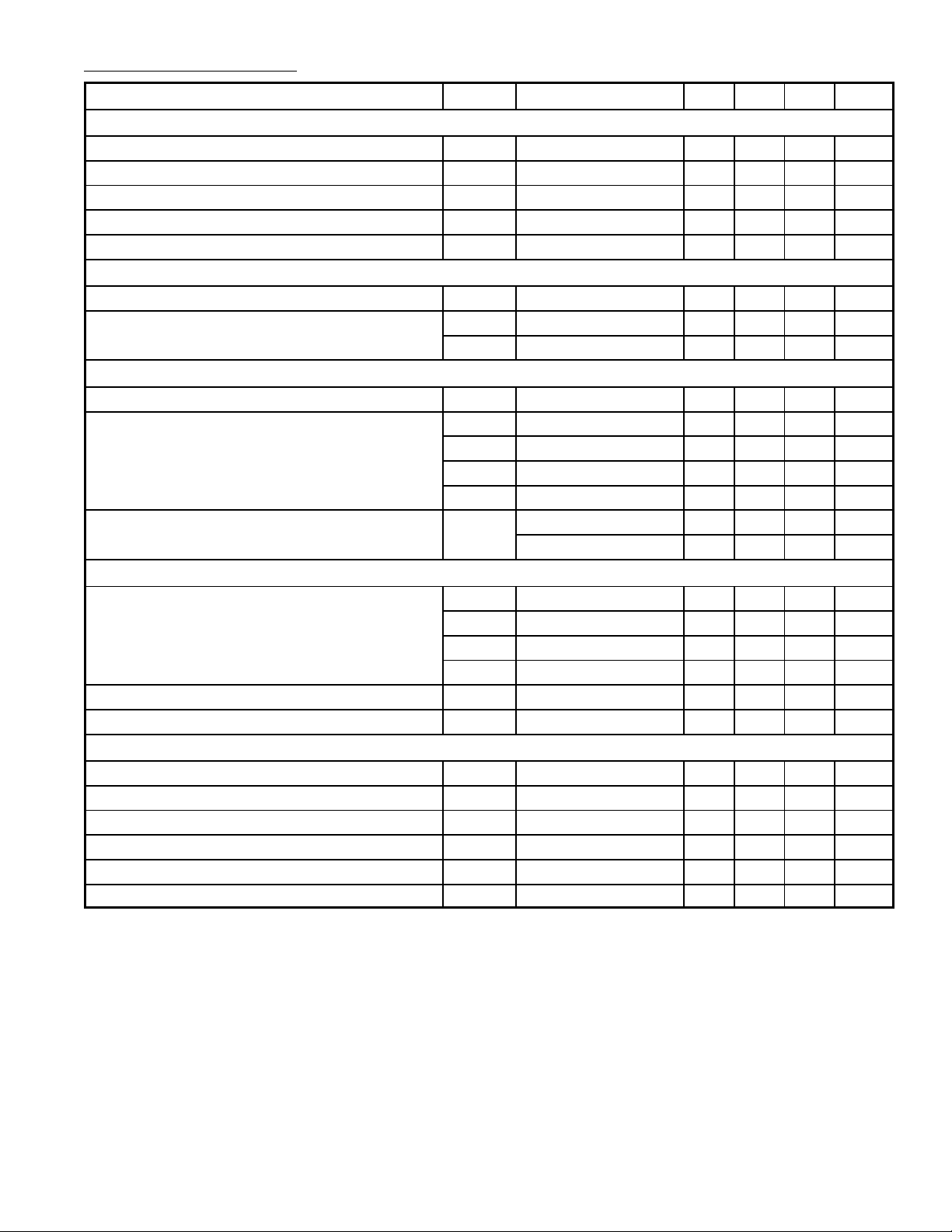
Electrical Characteristics: (TA = +25°C, VCC (V
) = 26V, Note 1, Note 3 unless otherwise specified)
9–4
Parameter Symbol Test Conditions Min Typ Max Unit
Supply
Supply Voltage, Pin9 V
Supply Voltage Output Stage V
9–4
6–4
Note 5 10 – 40 V
– – 60 V
Supply Current, Pin6 and Pin9 I6 + I9Note 6 35 55 85 mA
Quiescent Current I
4
25 40 65 mA
Variation of Quiescent Current with Temperature TC – –0.04 – mA/°C
Output Current
Output Current (Peak–to–Peak), Pin5 I
Output Current Flyback Generator, Pin8 +I
5(P–P)
8(P–P)
–I
8(P–P)
– 2.5 3.0 A
– 1.25 1.5 A
– 1.35 1.6 A
Output Voltage
Peak Voltage During Flyback V
Saturation Voltage to Supply V
V
V
V
Saturation Voltage to GND V
5–4
6–5(sat)I5
5–6(sat)I5
6–5(sat)I5
5–6(sat)I5
5–4(sat)I5
= –1.5A – 2.5 3.2 V
= 1.5A, Note7 – 2.5 3.2 V
= –1.2A – 2.2 2.7 V
= 1.2A, Note 7 – 2.3 2.8 V
= 1.2A – 2.2 2.7 V
– – 60 V
I5 = 1.5A – 2.5 3.2 V
Flyback Generator
Saturation Voltage V
9–8(sat)I8
V
8–9(sat)I8
V
9–8(sat)I8
V
8–9(sat)I8
Leakage Current at Pin8 –I
Flyback Generator Active If: V
8
5–9
= –1.6A – 1.6 2.1 V
= 1.5A, Note 7 – 2.3 3.0 V
= –1.3A – 1.4 1.9 V
= 1.2A, Note 7 – 2.2 2.7 V
– 5 100 µA
4 – – V
Input
Input Current, Pin1 I
Input Voltage During Scan, Pin1 V
Input Current During Scan, Pin3 I
Input Voltage During Scan, Pin3 V
Input Voltage During Flyback, Pin1 V
Input Voltage During Flyback, Pin3 V
1–2
3–2
1–2
3–2
I5 = 1.5A – 0.33 0.55 mA
1
– 2.35 3.0 V
Note 8 0.03 – – mA
3
Note 8 0.8 – V
– – 250 mV
– – 250 mV
9–4
V
Note 1. Pin2 and Pin4 are externally connected to GND.
Note 3. Pin1 externally connedted to Pin3.
Note 4. Non–repetitive duty factor 3.3%.
Note 5. The maximum supply voltage should be chosen so that during flyback the voltage at Pin 5
does not exceed 60V.
Note 6. When V
is 13V and no load at Pin5.
5–4
Note 7. Duty cycle, d = 5% or d = 0.05
Note 8. When Pin3 is driven separately from Pin1.
Page 3

Electrical Characteristics (Cont’d): (TA = +25°C, VCC (V
) = 26V, Note 1, Note 3 unless
9–4
otherwise specified)
Parameter Symbol Test Conditions Min Typ Max Unit
Guard Circuit
Output Voltage, Pin7 V
Internal Series Resistance of Pin7 Ri
Guard Circuit Activates V
General Data
Open Loop Gain G
Frequency Response f –3dB, Note 12 – 60 – kHz
7–2
8–2
RL = 100kΩ, Note 11 4.1 4.5 5.8 V
IL = 0.5mA, Note 11 3.4 3.9 5.3 V
7
Note 9 – – 1.0 V
at 1kHz, Note 10 – 33 –
O
0.95 1.35 1.7 kΩ
Note 1. Pin2 and Pin4 are externally connected to GND.
Note 3. Pin1 externally connedted to Pin3.
Note 4. Non–repetitive duty factor 3.3%.
Note 5. The maximum supply voltage should be chosen so that during flyback the voltage at Pin 5
does not exceed 60V.
Note 6. When V
is 13V and no load at Pin5.
5–4
Note 7. Duty cycle, d = 5% or d = 0.05
Note 8. When Pin3 is driven separately from Pin1.
Note 9. During normal operation the voltage V
Note10. R
= 8Ω; IL = 125mA
L
RMS
may not be lower than 1.5V
8–2
Note11. If guard circuit is active.
Note12. With a 22pF capacitor between Pin1 and Pin5.
Pin Connection Diagram
(Front View)
9
V
Flyback Generator
8
7
Voltage Stabilizer
6
Output Stage Supply Input
5
Output
4
Output Stage GND
3
Switching Circuit
2
GND
Input
1
CC
Page 4

.961 (24.4)
.780 (19.8)
91
.079
(2.0)
.100 (2.54)
.185 (4.7)
.489
(12.4)
.079
(2.0)
.674
(17.0)
 Loading...