

Page 1
NTE1747
Integrated Circuit
TV Video Processing Circuit
Description:
The NTE1747 is an integrated circuit in a 28–Lead DIP type package designed for color TV video and
chrominance signal processing circuit.
Features:
D Including Video and Chrominance Signal Processing Circuit on a Single Chip, for Compact Set
Design
D Including Circuit For Compensating Skin Color
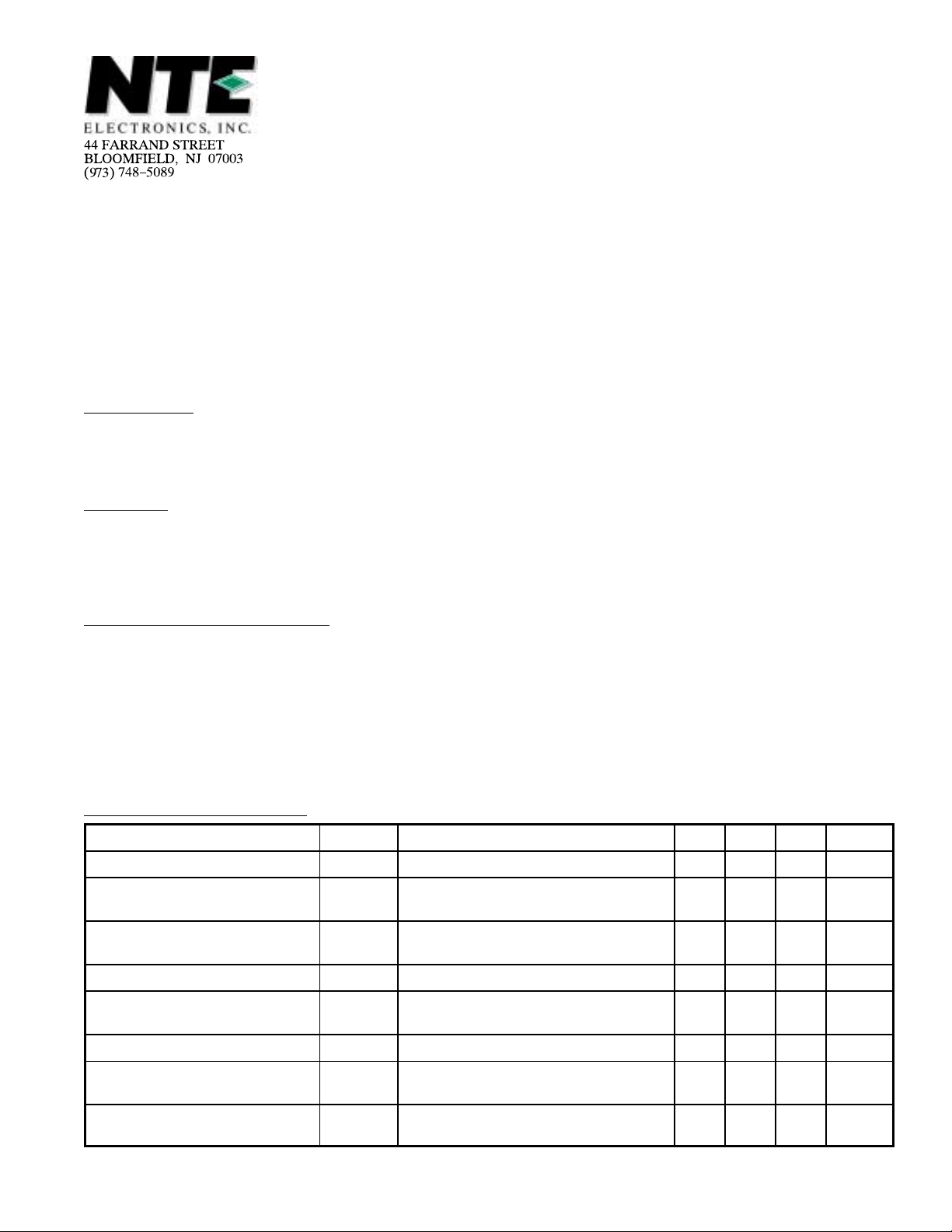
Absolute Maximum Ratings: (TA = +25°C unless otherwise specified)
Supply Voltage, V
Circuit Voltage, V
Circuit Current, I
Power Dissipation, P
CC
2,3,10,11–12,19,20,28–9
25,26,27,28,29
D
Operating Ambient Temperature Range, T
Storage Temperature Range, T
stg
opr
0V to +14.4V. . . . . . . . . . . . . . . . . . . . . . . . . . . . . . . . . . . . . . . . .
–40mA to 0mA. . . . . . . . . . . . . . . . . . . . . . . . . . . . . . . . . . . . . . . . . . . . . . .
–20° to +70°C. . . . . . . . . . . . . . . . . . . . . . . . . . . . . . . . . .
–55° to +150°C. . . . . . . . . . . . . . . . . . . . . . . . . . . . . . . . . . . . . . . . . .
+14.4V. . . . . . . . . . . . . . . . . . . . . . . . . . . . . . . . . . . . . . . . . . . . . . . . . . . . . . . . . . . . .
1200mW. . . . . . . . . . . . . . . . . . . . . . . . . . . . . . . . . . . . . . . . . . . . . . . . . . . . . . . . .
Electrical Characteristics
Parameter Symbol Test Conditions Min Typ Max Unit
Total Circuit Current I
Demodulation Color Difference
Output Voltage
Demodulation Color Difference
Output Voltage
ACC Characteristics ACC Rainbow 15mV
Oscillation Frequency f
f
Change with Supply Voltage Df
osc
f
Change with Ambient
osc
Temperature
Control Sensitivity b Change to Pin18 Df when V1 (8.6V) and
: (TA = +25°C unless otherwise specified)
tot
e
o(max)
e
o(typ)
osc
osc/VCCVCC
Df
osc/TATA
VCC = 12V 40 54 67 mA
Rainbow 150mV
Color Max.
Rainbow 150mV
Color Typ.
Difference between Pin8 input invalid
signal & standard sample
= 12V ±20%, for VCC = 12V – – 120 Hz
= –20° to +70°C, for TA = +25°C 0 1.5 2.5 Hz/deg.
(8.2V) are applied to Pin15.
V
2
, Contrast Max.,
P–P
, Contrast Max.,
P–P
, ACC–eo Typ 0.65 0.88 1.05 times
P–P
4.6 5.3 6.0 V
1.35 1.75 2.15 V
– – ±150 H
1.9 2.5 3.2 Hz.mV
p–p
p–p
z
Page 2
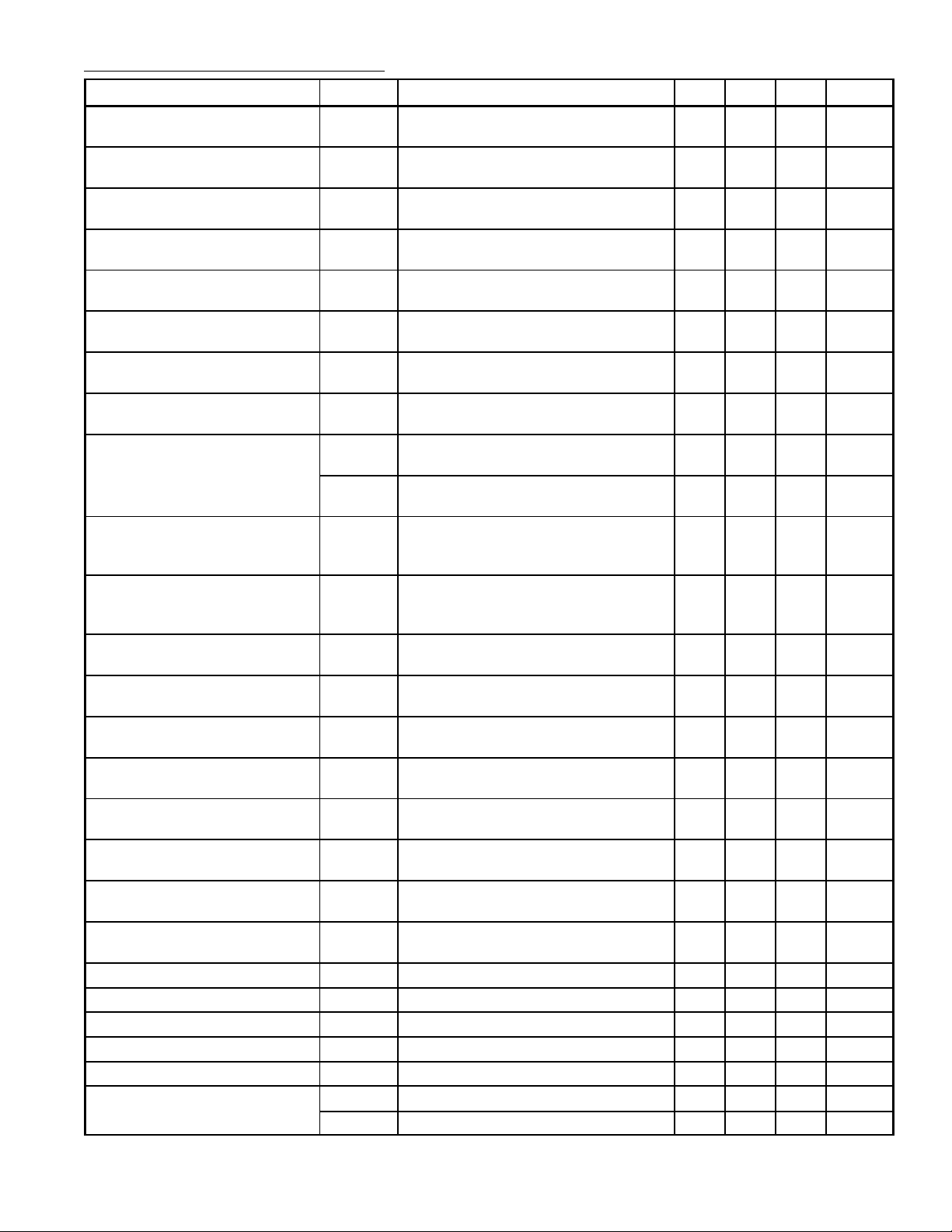
Electrical Characteristics (Cont’d): (TA = +25°C unless otherwise specified)
Parameter Symbol Test Conditions Min Typ Max Unit
Phase Detector µ Apply D0–changed frequency for burst
phase to Pin18.
Phase Hold Characteristics Df Df = 1 (m.b) x 100 – 1.0 1.6 deg/
APC Pull–in Range f
APC
Rainbow 150mV
measured by
P–P
changing burst frequency
Demodulation Output Ratio R/B Demodulator input 0.5V
P–P
,
f = 3.59MHz
Demodulation Output Ratio G/B Demodulator input 0.5V
P–P
,
f = 3.59MHz
Demodulation Angle <R Demodulator input 0.5V
P–P
,
f = 3.59MHz, LB = 0dg
Demodulation Angle <G Demodulator input 0.5V
P–P
,
f = 3.59MHz, LB = 0dg
Color Killer Level e
Attenuation from rainbow 150mV
k
(=0dB) to killer operation
Video Voltage Amplification A
V1
Sine wave input 0.3V
at 20kHz,
P–P
contrast max., picture min.
A
V2
Sine wave input 0.3V
at 20kHz,
P–P
contrast 75%
DC Transfer Rate T
DC
Video input 0.5V
(stair step),
P–P
APL10 % to 90%. Contrast max.
Picture min.
Differential Gain DG Video input 0.5V
(stair step),
p–p
APL10 ∼ 90%. Contrast max.
picture min.
Demodulation DC Output Voltage E
O(DC)
Input invalid signal, VCO oscillation,
demodulator outputs
DC Voltage Difference Between
Demodulation Outputs
DEO Change with Supply Volt-
age
DEO Change with Ambient
DE
X–Y
DE
X–Y/VC
C
DE
X–Y/TATA
Differential voltage of demodulator
outputs
VCC = 12V ± 20%, for VCC = 12V – 0 ±60 mV
= –20 ∼ +70°C. for TA = +25°C – 0 ±60 mV
Temperature
AIC Switching Level V
SW
f = 3.58MHz, Pin21 level when
Pin 0 = 10V
Chroma Voltage Gain G
Vchroma
Chroma/Burst 350/150mV
P–P
,
Phase 123
AIC Voltage Gain G
vAIC
Chroma/Burst 200/150mV
P–P
,
Phase 123’ color killer OFF
AIC Sensitivity S
AIC
Chroma/Burst 300/100mV
P–P
,
Phase 0 tint center
Phase Compensation Center Q
Phase Compensation Range Q
Phase Compensation Range Q
Phase Compensations Quantity Q
Phase Compensations Quantity Q
Max. Phase Compensation
Quantity
Q
Qmax1
Q
Qmax2
c1
c2
Q1
Q2
0
Chroma/Burst 150mV
P–P
Color Compensation ON 17 21.5 26 deg.
27 46 64 mV/deg
±550 ±800 – Hz
0.84 0.93 1.02 times
0.25 0.29 0.33 times
86.5 90.0 94.5 deg.
229 236 243 deg.
–35 –40 –45 dB
P–P
7.0 7.7 8.4 times
6.3 7.0 7.6 times
86.0 90.5 95.0 %
– – 5 %
7.20 7.60 8.05 V
– – 300 mV
160 260 340 mV
1.6 2.2 2.7 V
14.5 19.0 23.5 dB
0.7 1.15 1.5 V
115 123 134 deg.
100 112 124 deg.
–108 –120 –132 deg.
–18 –22.5 –28 deg.
51 59 67 deg.
–55 –63 –71 deg.
100Hz
p–p
p–p
p–p
Page 3

Pin Connection Diagram
Pedestal Clamp Filter
Brightness Control
Contrast Control
Blank Level Filter
Video Signal Input (1)
Video Signal Input (2)
Chrominance Signal Bypass
Chrominance Signal Input
GND
Color Control
Tint Control
Burst Gate Pulse Input
V
CC
ACC Filter
1
2
3
4
5
6
7
8
9
10
11
28
27
26
25
24
23
22
21
20
19
18
12 17
13 16
14
15
Picture Control
B – Y Demod Output
G – Y Demod Output
R – Y Demod Output
VCO Filter
Video Signal Output
VCO Filter
AIC Input
Blanking Pulse Input
AIC Color Compensation Switch
VCO Input
VCO Output
Color Killer Filter
APC Filter
14 1
15 28
1.469 (37.32) Max
.100 (2.54)
1.300 (33.02)
.250
(6.35)
.122
(3.1)
Min
.540
(13.7)
.600 (15.24)
 Loading...