

Page 1

NTE1537
Integrated Circuit
CMOS, Digital Frequency Indicator
w
/Clock LED Function
Applications:
D Car Radio Applications: FM/AM Receiving Frequency Display and Clock Display
D Home Radio Applications: FM/AM Receiving Frequency Display and Clock Display
D Car Clock Applications: Hours–Minutes, Month–Date/Stopwatch Display
Functions:
D FM Receiving Frequency Display (4 Digits)
D AM Receiving Frequency Display (4 Digits)
D Month–Date or Stopwatch Display (Either of these Selectable)
Features:
D Single–Chip CMOS LSI for Static Display System
D Capable of Direct Driving Green LED (Drive Capacity 15mA)
D Capable of Selecting Frequency Display/Time Display
D Use FM/AM Local Oscillation Signal of Varactor Diode, Variable Capacitor, or µ Tuning System
to Digitally Display FM/AM Receiving Frequency
D Covers 4 AM Intermediate Frequencies: +262.5, +452.5, +455, +470kHz
D Covers 2 FM Intermediate Frequencies: +10.7, –10.7MHz
D Capable of Fine–Adjusting AM/FM Display Frequency Error Independently
• A variable Resistor can be used to Correct AM IF Error within ±2.8kHz
• A variable Resistor can be used to Correct FM IF Error within ±140kHz
D Two Selections of Display System (12–Hour System with PM Sign which is Displayed During
Setting Only, 24–Hour System)
D Programmed on Long Months (31 Days)/Short Months (30 Days). Date in February is Pro-
grammed to Count up to the 29
D Easy to Set Time by th Time Signal
D Stopwatch Capable of Counting/Displaying 1 Second to 12 Hours, 59 Minutes, 59 Seconds
D Inhibit Pin for Inhibiting Time Setting with Display Unlighted
D 4MHz Crystal for Reference Frequency
th
Page 2
Absolute Maximum Ratings: (TA = +25°C, VSS = 0V unless otherwise specified)
Maximum Supply Voltage, VDDmax –0.3 to 11V. . . . . . . . . . . . . . . . . . . . . . . . . . . . . . . . . . . . . . . . . . . .
(Cumulative applied time: 30min or less) –0.3 to 14V. . . . . . . . . . . . . . . . . . . . . . . . . . . . . . . . .
Reference Voltage (V
≤ VDD), V
ref
ref
–0.3 to 10V. . . . . . . . . . . . . . . . . . . . . . . . . . . . . . . . . . . . . . . . . . .
(Cumulative applied time: 30min or less) –0.3 to 13V. . . . . . . . . . . . . . . . . . . . . . . . . . . . . . . . .
Input Voltage, V
I
Output Voltage (Output OFF), V
O
–0.3 to VDD+0.3V. . . . . . . . . . . . . . . . . . . . . . . . . . . . . . . . . . . . . . . . . . . . . . . . . . . . . . .
–0.3 to VDD+0.3V. . . . . . . . . . . . . . . . . . . . . . . . . . . . . . . . . . . . . . . . .
Allowable Power Dissipation (TA ≤ +75°C), PDmax 800mW. . . . . . . . . . . . . . . . . . . . . . . . . . . . . . . . . . .
Allowable Power Disipation of Segment Output, PD(seg)
Other than PM: IOL < 25mA 15mW. . . . . . . . . . . . . . . . . . . . . . . . . . . . . . . . . . . . . . . . . . . . . . . . .
PM: IOL < 75mA 45mW. . . . . . . . . . . . . . . . . . . . . . . . . . . . . . . . . . . . . . . . . . . . . . . . . . . . . . . . . . .
Operating Temperature Range, T
Storage Temperature Range, T
stg
opr
–30° to +75°C. . . . . . . . . . . . . . . . . . . . . . . . . . . . . . . . . . . . . . . . .
–40° to +125°C. . . . . . . . . . . . . . . . . . . . . . . . . . . . . . . . . . . . . . . . . .
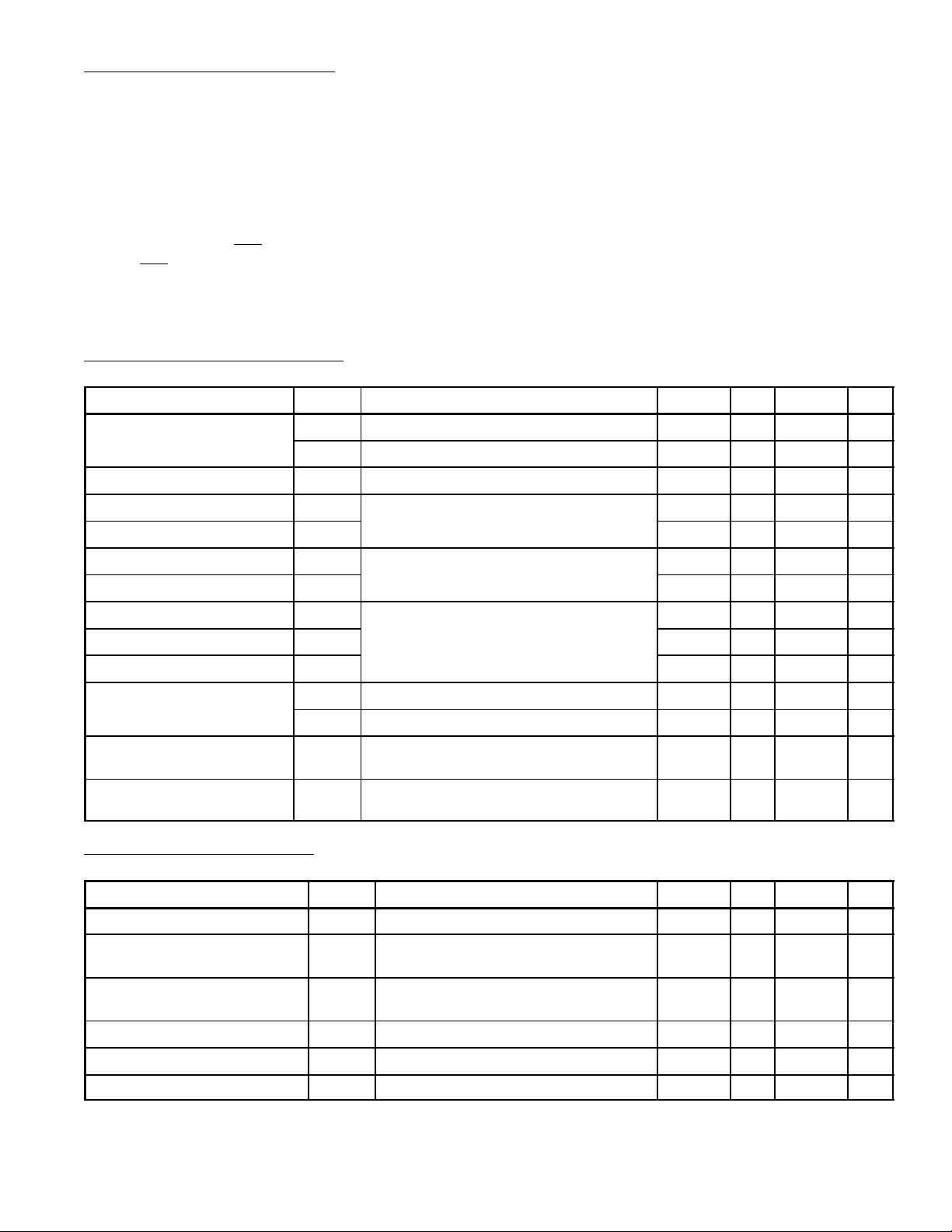
Allowable Operating Ranges: (TA = +25°C, VDD = 8 to 10.3V, VSS = 0V, V
V
= 0V if VDD < 8V unless otherwise specified)
ref
Parameter Symbol Test Conditions Min Typ Max Unit
Supply Voltage V
V
Reference Voltage V
Input “H” Level V oltage V
Input “L” Level V oltage V
Input “H” Level V oltage V
Input “L” Level V oltage V
Input “H” Level V oltage V
Input “L” Level V oltage V
Input “M” Level V oltage V
Input Frequency f
Operating Frequency f
Input Amplitude V
DD1
DD2
IN1
f
IN2
opg
P–P
All function operating mode 8.0 9.3 10.8 V
Only clock operating mode 4.3 5.0 8.0 V
V
ref
IH1
IL1
IH2
IL2
IH3
IL3
IM
≤ V
ref
DD
INHI, VDD = 4.3 to 10.3V 0.75V
FM/AM, IF–FM, IF–AM1, IF–AM2, 12H/24H 0.85V
SET, DEMAND, CTR/CLK 0.88V
Fin–FM, V
Fin–AM, V
= 0.7V, Duty 50% 0.6 – 2.0 MHz
P–P
= 0.7V, Duty 50% 0.4 – 2.5 MHz
P–P
Crystal is externally connected across
7.9 8.0 9.0 V
DD
V
SS
DD
V
SS
DD
V
SS
0.36V
DD
3.5 – 4.2 MHz
OSC–IN and OSC–OUT
Fin–FM, Fin–AM, Ceramic capacitor of
0.4µF is connected across VDD an V
SS
0.7 – – V
= 7.9 to 9V ≤ VDD,
ref
– V
– 0.1V
– V
– 0.15V
– V
– 0.12V
– 0.64V
DD
DD
DD
DD
DD
DD
DD
V
V
V
V
V
V
V
P–P
Electrical Characteristics: (TA = +25°C, VDD = 8 to 10.3V, VSS = 0V, V
V
ref
≤ V
unless otherwise specified)
DD
Parameter Symbol Test Conditions Min Typ Max Unit
Input Current I
Input “H” Level Current I
Input “L” Level Current I
IH1
FM–Fine, AM–Fine, VIN = 0V or V
IN
IF–FM, IF–AM1, IF–AM2, CTR/CLK,
12H/24H, VIN = 0.9V
IF–FM, IF–AM1, IF–AM2, CTR/CLK,
IL1
DD
ref
12H/24H, VIN = 0V
Input “H” Level Current I
Input “L” Level Current I
Middle Point Setting Resistance r
IH2
FM/AM, VIN = 0.9V
FM/AM, VIN = 0V –3 – 0 µA
IL2
SET, DEMAND 40 70 100 kΩ
s
DD
Note 1. + sign: Flowing into LSI
– sign: Flowing out of LSI
= 7.9 to 9V,
ref
–1 – +1 µA
–80 –30 –10 µA
–3 – 0 µA
–40 –15 –5 µA
Page 3

Electrical Characteristics (Cont’d): (TA = +25°C, VDD = 8 to 10.3V, VSS = 0V, V
V
≤ V
ref
Parameter Symbol Test Conditions Min Typ Max Unit
unless otherwise specified)
DD
= 7.9 to 9V,
ref
Input Floating Voltage V
Input “H” Level Current I
Input Floating Voltage V
IF3
IH4
IF4
Feedback Resistance Rf
Rf
Rf
Output “L” Level V oltage V
Output Leakage Current I
Current Dissipation I
V
OFF
DD1
I
DD2
OL1
OL2
I
ref
Note 1. + sign: Flowing into LSI
– sign: Flowing out of LSI
SET, DEMAND, input floating 0.45V
INHI, VDD = 4.3 to 10.3V, VIN = V
DD
15 – 400 µA
DD
– 0.55V
INHI, VDD = 4.3 to 10.3V, input floating 0 – 0.3 V
Feedback resistance across OSC–IN
1
– 3 – MΩ
and OSC–OUT
Feedback resistance of Fin–FM – 3 – MΩ
2
Feedback resistance of Fin–AM – 3 – MΩ
3
PM, VDD = 8V, IOL = 45mA – – 0.7 V
Segment outputs other than PM
– – 0.7 V
VDD = 8V, IOL = 15mA
All segment outputs, VDD = 10.3V,
– – 10 µA
VOH = 10.3V
VDD = 10.3V, f
mounted), f
VDD = 5.5V, f
mounted), V
VDD = 10.3V, V
AM–Fine = FM–Fine = V
= 4MHz (with crystal
opg
= 2.5MHz (0.7V
IN2
= 4MHz (with crystal
opg
= 0V, INHI = 0
ref
= 9V,
ref
ref
P–P
– 8 17 mA
)
– 1.0 2.5 mA
– 0.5 1.5 mA
DD
V
Pin Connection Diagram
Seg – d Digit 4
Seg – c Digit 4
Seg – g Digit 4
Seg – b Digit 4
IF – AM 2
V
FM/AM
FM – Fine
AM – Fine
INHI
12/24 H
OSC Output
V
DD
1
2
3
4
5FIN – FM
6FIN – AM
7IF – FM
8
9 34
ref
10IF – AM 1
11
12 31
13
14CTL/CLD 29
15SET 28
16Demand
17
18 25
19
20OSC Input 23
21 22
42
Seg – e Digit 4
Seg – f Digit 4
41
40
Seg – a Digit 4
39
Seg – b Digit 3
38
Seg – g Digit 3
Seg – c Digit 3
37
36
V
SS
Seg – d Digit 3
35
Seg – e Digit 3
Seg – f Digit 3
33
Seg – a Digit 3
32
Seg – b Digit 2
30
Seg – g Digit 2
Seg – c Digit 2
Seg – d Digit 2
27
Seg – e Digit 2
26
Seg – f Digit 2
Seg – a Digit 2
24
Seg – b Digit 1
Seg – c Digit 1
Seg – PM Digit 1
Page 4

42 22
121
.100 (2.54)
2.094 (53.2)
2.000 (50.8)
.204
(5.18)
.157
(3.9)
.543 (13.8)
.598 (15.2)
 Loading...