

Page 1
NTE1410
Integrated Circuit
Chroma Video Signal Processor
Description:
The NTE1410 is an integrated circuit in a 28–Lead DIP type package designed for all color TV video
and chrominance signal process circuits.
Features:
D The NTE1410 provides a total video and chrominance signal processing circuitry, allowing
compact set design
D Incorporating luminance signal mixing circuit and provides R.G.B. original color output
D All DC control system for simplicity of wiring (color, tint, contrast, picture, luminance)
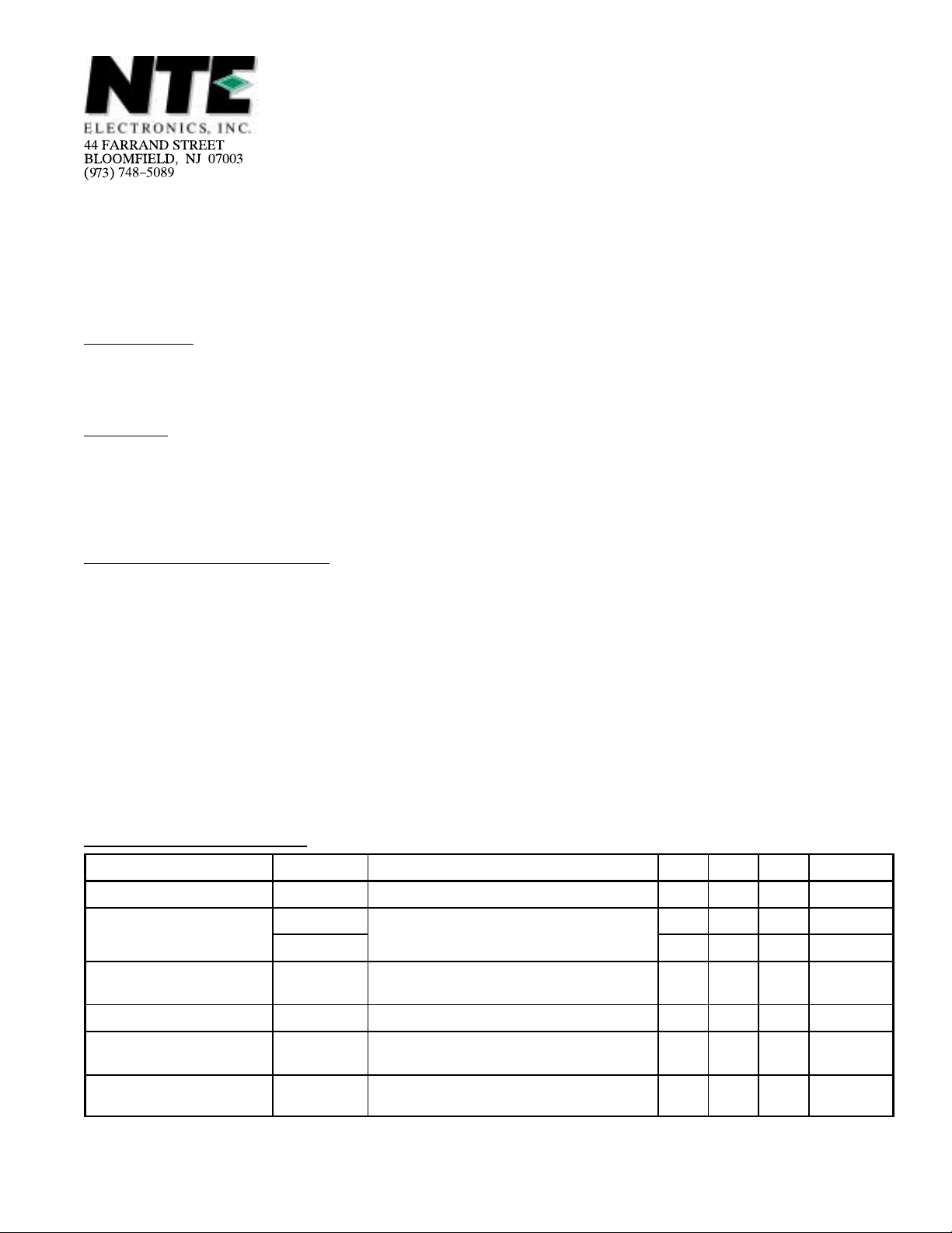
Absolute Maximum Ratings
Supply Voltage, V
CC
: (TA = +25°C unless otherwise specified)
Circuit Voltage
V
1–14
V
3,4,7,8,9,10–14
V
20–14
V
24–14
. . . . . . . . . . . . . . . . . . . . . . . . . . . . . . . . . . . . . . . . . . . . . . . . . . . . . . . . . . . . . . . . . . . . .
. . . . . . . . . . . . . . . . . . . . . . . . . . . . . . . . . . . . . . . . . . . . . . . . . . . . . . . . . . . . . .
Circuit Current, I
Power Dissipation (T
Operating Ambient Temperature Range, T
Storage Temperature Range, T
. . . . . . . . . . . . . . . . . . . . . . . . . . . . . . . . . . . . . . . . . . . . . . . . . . . . . . . . .
, I27, I
26
28
= +70°C), PD 750mW. . . . . . . . . . . . . . . . . . . . . . . . . . . . . . . . . . . . . . . . . . . . . .
A
opr
stg
Note 1. and are flow–in and flow–out currents to/from the circuit, respectively.
Electrical Characteristics
Parameter Symbol Test Conditions Min Typ Max Unit
Total Circuit Current I
Circuit Voltage V
Output Voltage (Burst) V
: (TA = +25°C unless otherwise specified)
tot
11–14
V
26, 27, 28–14
O(1)
VCC = 12V 33 44 56 mA
VCC = 12V 7.5 8.5 9.2 V
Rainbow 150mV
Contrast Max.
, Color AUTO Center,
P–P
3.5 4.0 4.5 V
0.5 0.7 0.9 V
0V to 14.4V. . . . . . . . . . . . . . . . . . . . . . . . . . . . . . . . . . . . . . . . . . . . . . . . . . . . . . . . . . . . . . . .
0V to V
–6V to V
–20° to +70°C. . . . . . . . . . . . . . . . . . . . . . . . . . . . . . . . . .
–40° to +125°C. . . . . . . . . . . . . . . . . . . . . . . . . . . . . . . . . . . . . . . . . .
–40mA. . . . . . . . . . . . . . . . . . . . . . . . . . . . . . . . . . . . . . . . . . . . . . . . . . . . . . . .
14.4V. . . . . . . . . . . . . . . . . . . . . . . . . . . . . . . . . . . . . . . . . . . . . . . . . . . . . . . . . . . . . .
V
P–P
1–14
1–14
1–14
ACC Characteristics ACC Rainbow 15mV
Output Voltage (Chroma) V
Oscillation Frequency f
O(2)
OSC
Rainbow 150mV
Max.
Pin13 Input Invalid Signal, Trimmer to be
Set by Standard Samples, Note 2
Note 2. f: Deviation from 3579545Hz.
, Burst Output/V
P–P
, Color Max., Contrast
P–P
O(1)
0.6 0.8 1.0 times
0.5 0.7 0.9 V
– – ±150 Hz
P–P
Page 2
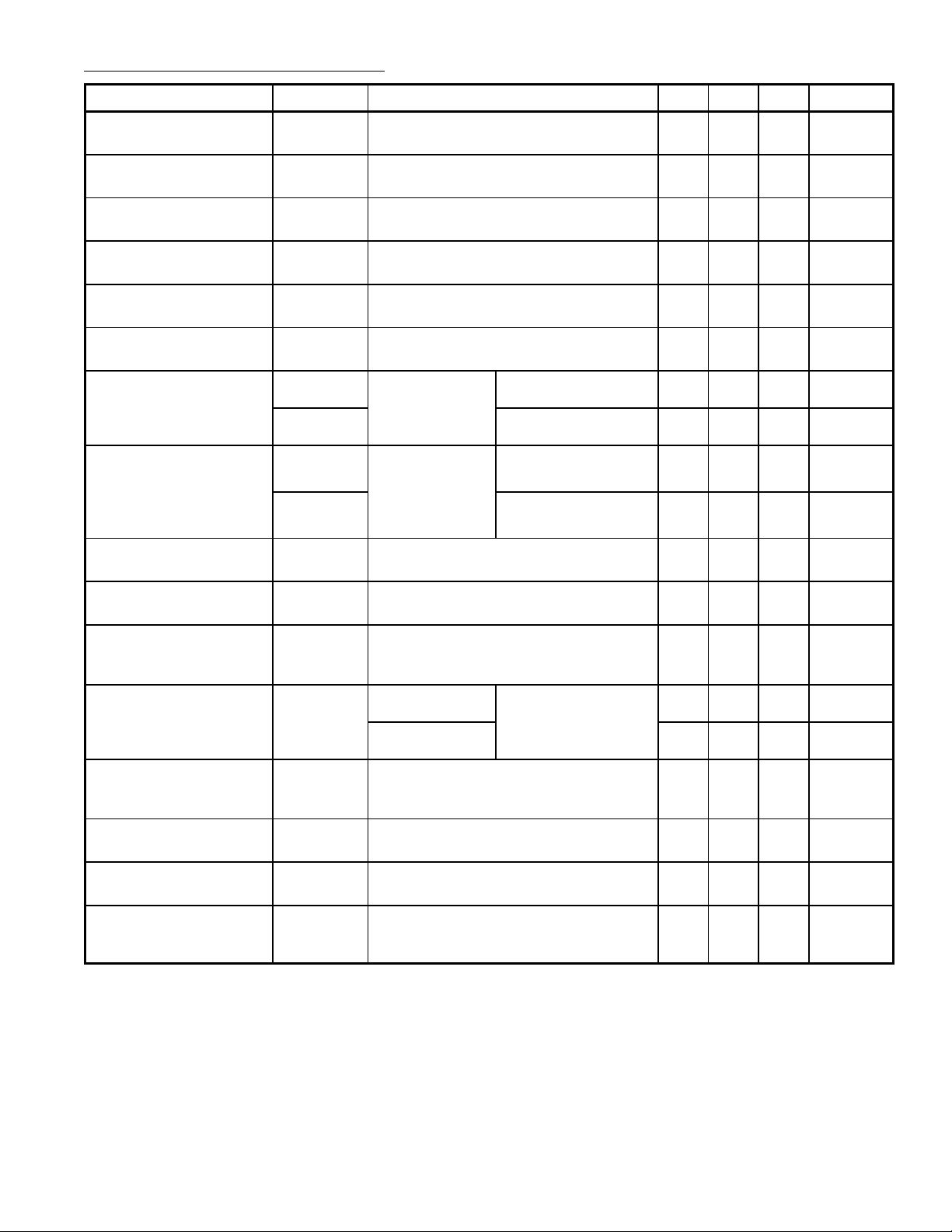
Electrical Characteristics (Cont’d): (TA = +25°C unless otherwise specified)
∠
Parameter Symbol Test Conditions Min Typ Max Unit
f
Drift with
OSC
Supply Voltage
f
Drift with
OSC
Ambient Temperature
Df
OSC/VCC
Df
OSC/TA
Pin16 and pin17 Short–Circuit, VCC = 12V,
Note 3
TA = –20° to +70°C, Pin16 an d P in17 S hort–
Circuit, IC Unit, Note 4
– – ±60 Hz
0 –1 –2 Hz/deg.
Control Sensitivity (VCO) b Burst Input 0.7V
for 100Hz V ariation
Phase Detector Sensitivity m Burst Input 0.7V
Phase Hold
Characteristics
APC Pull–In Range f
Error and V
DF Burst Input 0.7V
Variation
APC
Burst Input 0.7V
16–17
Changed for Measurement
Demodulation Output
Ratio
Ratio
Demodulation Angle
R/B
G/B
∠ R
(1)
(2)
Demodulation
Input 0.2V
Input 0.2V
P–P
P–P
f = 3.59MHz,
Note 5
Demodulation
Input 0.2V
P–P
,
,
,
B = 0 deg.,
∠ G
f = 3.59MHz,
Note 5
Color Difference Output
Voltage (Max)
Total Color Difference
Output Voltage
Color Killer Level e
e
e
O(1)
O(2)
K
Demodulator Input 1.2VP, f = 3.5 9 M H z, B R
Output, Note 5
Rainbow 150mV
Contrast Max., R Output, Note 6
Attenuation of Pin13 Input Burst Voltage at
Killer Operating (Burst Voltage 150mV =
0dB), Note 6
, Calculation with V
P–P
, Calculation with Phase
P–P
16–17
1.2 1.5 2.0 Hz/mV
25 45 55 mV/deg.
for 100Hz Change
, Phase Error for 100Hz
P–P
, Burst Frequency to be
P–P
R Output/e
G Output/e
0
0
– 1.5 2.5 deg/100Hz
±450 ±600 – Hz
0.86 0.94 1.04 times
0.25 0.30 0.35 times
R–B Phase Difference 94.0 97.5 102 deg.
G–B Phase Difference 228 235 242 deg.
4.8 5.7 – V
, AUTO Color Center,
P–P
1.28 1.70 2.13 V
–27 –32 –40 dB
P–P
P–P
Voltage Amplification
(Video)
(Video)
Frequency Characteristics
(Video)
A
V
Note 2
f
C
Sine Wave 0.1mV
cy in which A
Studio Color Bar White
Level 1V
Level 1V
, Contrast
, Contrast
P–P
P–P
Max., Picture Min.,
Note 7
Input, Input Frequen-
rms
becomes –6dB, Picture
V1
4.5 5.0 5.5 times
4.6 5.1 5.6 times
5 6 – MHz
Min., B Output, Note 6
DC Transfer Rate T
DC
Video Input, 1V
(Stair–Step),
P–P
68 75 82 %
APL 10 to 90%, B Output
Original Color Output
Voltage (Max.)
Differential Gain DB Video Input 1V
E
O
Output Voltage of each R, G, and B
at V
= 1.2V
3
(Stair–Step, 3.58MHz),
P–P
7.0 – – V
– – 5.0 %
APL 50%, Contrast Max., Picture Max.,
Note 7
Note 2. f: Deviation from 3579545Hz.
Note 3. Max. Width of Variation.
Note 4. Max. Width of Variation 90°C.
Note 5. A
Note 6. V
= 3.5V, Brightness VR Setting, No Blanking.
24
= 3.5V, Brightness VR Setting.
26
Note 7. Outputs of each R, G, and B, Pin26: Pedestal 2V, Brightness VR Setting.
Page 3

Electrical Characteristics (Cont’d): (TA = +25°C unless otherwise specified)
Parameter Symbol Test Conditions Min Typ Max Unit
Differential Gain DB Video Input 1V
(Stair–Step, 3.58MHz),
P–P
– – 5.0 %
APL 50%, Contrast Max., Picture Max.,
Note 7
Demodulation DC Output
Voltage
DC Voltage Difference
between Demodulation
E
O(DC)
DE
X–Y
VCO Oscillation, Output of each R, G, and
B, Note 8
V26 = 3.5V, VCO Oscillation, Outputs of
each R, G, and B
2.8 3.5 4.2 V
– 0 300 mV
Outputs
DE
Change with
X–Y
Supply Voltage
DE
Change with
X–Y
Ambient Temperature
DE
X–Y/VCCVCC
DE
X–Y/TA
= 12V ±20%, V26 = 3.5V (VCC = 12V)
for V
= 12V, Note 9
CC
V26 = 3.5V (TA = +25°C),
= –20° to +70°C, for TA = +25°C
T
A
– 0 ±60 mV
– 0 ±60 mV
Note 7. Outputs of each R, G, and B, Pin26: Pedestal 2V, Brightness VR Setting.
Note 8. Blanking ON.
Note 9. No Blanking.
Pin Connection Diagram
V
CC
Pedestal Clamp Filter
Brightness Control
Picture Control
Auto/Manual Switch
BPA Output
Chroma Bypass
Chroma Input
1
2
3
4
5Video Peaking
6Picture Peaking
7Tint Control
8
9Color Control 20
10Contrast Control
11
12 17
13
14GND 15
B Output
28
27
G Output
26
R Output
25
Demodulator Input
24 Blanking Pulse Input
23
3.58MHz OSC Filter
22
3.58MHz OSC Input
21
3.58MHz OSC Output
Burst Gate Pulse Input
19
APC Killer Filter
18
Color Killer Filter
APC Filter
16
APC Filter
APC Filter
14 1
15 28
1.469 (37.32)
Max
.100 (2.54)
1.300 (33.02)
.250
(6.35)
.122
(3.1)
Min
.540
(13.7)
.600
(15.24)
 Loading...