

Page 1
240 Output LCD Segment/Common Driver
Features
(Segment mode)
Shift Clock frequency:
!
20 MHz (Max.) (V
12 MHz (Max.) (V
Adopts a data bus system
!
4-bit/8-bit parallel input modes are selectable with a
!
mode (MD) pin
Automatic transfer function with an enable signal
!
Automatic counting function when in "chip select" mode,
!
which causes the internal clock to be stopped by
automatically counting 240 bits of input data
(Common mode)
Shift clock frequency :
!
4.0 MHz (Max.)
Built-in 240-bits bidirectional shift register (divisible into
!
120-bits x 2)
General Description
The NT7704 is a 240-bit output segment/common driver LSI
suitable for driving large scale dot matrix LCD panels used
by PDA's, personal computers and work stations for
example. Through the use of COG technology, it is ideal for
substantially decreasing the size of the frame section of the
LCD module. The NT7704 is good as both a segment driver
and as a common driver, and a low power consuming, high-
= 5 V ± 10%)
DD
= 2.5V - 4.5V)
DD
Available in a single mode (240-bits shift register) or in a
!
NT7704
dual mode(120-bits shift register x 2)
1. Y1 → Y240 Single mode
2. Y240 → Y1 Single mode
3. Y1 → Y120, Y121 → Y240 Dual mode
4. Y240 → Y121, Y120 → Y1 Dual mode
The above 4 shift directions are pin-selectable
(Both for segment mode and common mode)
Supply voltage for LCD driver: 15.0 to 30.0 V
!
Number of LCD driver outputs: 240
!
Low output impedance
!
Low power consumption
!
Supply voltage for the logic system: +2.5 to +5.5 V
!
COMS process
!
Package: Gold bump die / 272 Pin TCP(Tape Carrier
!
Package)
Not designed or rated as radiation hardened
!
precision LCD panel display can be assembled using the
NT7704. In the segment mode, the data input is selected as
4bit parallel input mode or as 8bit parallel input mode by a
mode (MD) pin. In the common mode, the data input/output
pins are bi-directional and the four data shift directions are
pin-selectable.
Pin Configuration
D
Y
Y
Y
Y
U
2
M
4
M
0
Y
Y
2
2
2
2
3
3
3
3
9
8
7
6
270 269 268272
Y
Y
1
1
2
2
2
3
Y
Y
Y
Y
1
1
1
1
1
1
2
2
8
9
0
1
152153154155 150 34
Y5Y4Y3Y2Y
D
U
M
M
1
Y
353637271
33151
NT7704
123456789101112131415161718192021222324252627 28 29 30 31 32
D
U
M
M
Y
V
V
V
V
V
5
4
0
0
1
L
3
L
L
2
L
L
D0D1D2D3D4D5D6D7LPE
V
V
S
E
S
D
/
I
S
D
C
O
2
FRMDNCV
D
X
I
I
C
O
S
K
1
P
O
F
F
NCV
L
/
R
5
S
R
S
1V1.0
D
V
V
V
V
U
0
0
4
1
M
R
R
3
2
M
R
R
Y
Page 2
Pad Configuration
x
x
433
448
ALK_L
x
1
Block Diagram
NT7704
x
Dummy Pad
NT7704
225432
x
ALK_R
208
x
224
209
x
DISPOFF
EIO
EIO
XCK
L/R
MD
S/C
V
V
0R
FR
1
2
LP
Level
Shifter
Active
Control
Control
Logic
43R
12R
V
5R
Y1 Y2 Y239 Y240V
240 Bits 4 Level Driver
/240
240 Bits Level Shifter
/240
240 Bits Line Latch/Shift Register
8Bits2
Data
Latch
V
5L
43L
V
12L
V
0L
V
/16/16 /16 /16 /16
Data Latch Control
/8
SP Conversion & Data Control
(4 to 8 or 8 to 8)
D0D1D2D3D4D5D6D
7
V
VSSV
DD
SS
2
Page 3
Pad Description
Pad No. Designation I/O Description
1 - 12 V
13 - 20 V
21 -28 V
29 - 40 V
41 - 66 V
67 - 92 V
0L
12L
43L
5L
SS
DD
93 - 94 S/C I Segment mode/common mode selection
95 - 97 EIO
2
P Power supply for LCD driver
P Power supply for LCD driver
P Power supply for LCD driver
P Power supply for LCD driver
P Ground (0V), these pads must be connected to each other
P Power supply for the logic system (+2.5 to +5.5V)
I/O Input/output for chip select or data of the shift register
NT7704
98, 99, 100 -
116, 117, 118
D0 - D6 I Display data input for segment mode
119 - 121 D7 I Display data input for Segment mode/ Dual mode data input
122 - 124 XCK I Display data shift clock input for segme nt mode
125 - 127
DISPOFF
I Control input for deselect output level
128 - 130 LP I Latch pulse input/shift clock input for the shift register
131 - 133 EIO
1
I/O Input/output for chip select or data of the shift register
134 - 136 FR I AC-converting signal input for LCD driver waveform
137 - 139 L/R I Display data shift direction selection
140 - 142 MD I Mode selection input
143 - 168 V
169 - 180 V
181 - 188 V
189 - 196 V
197 - 208 V
SS
5R
43R
12R
0R
P Ground (0V), these pads must be connected to each other
P Power supply for LCD driver
P Power supply for LCD driver
P Power supply for LCD driver
P Power supply for LCD driver
209 - 448 Y1 - Y240 O LCD driver output
3
Page 4
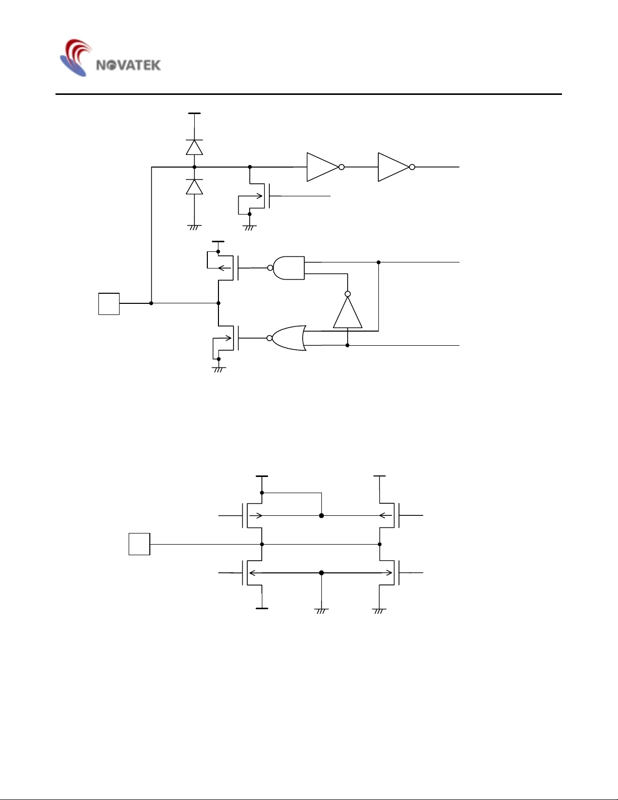
Input / Output Circuits
NT7704
DD
V
I
Input Signal
Applicable Pins
L/R, S/C, D0 - D6,
, LP, FR, MD
SS
V
Input Circuit (1)
DD
V
I
Control Signal
SS
V
SS
V
DISPOFF
Input Signal
Applicable Pins
D7, XCK
Input Circuit (2)
4
Page 5
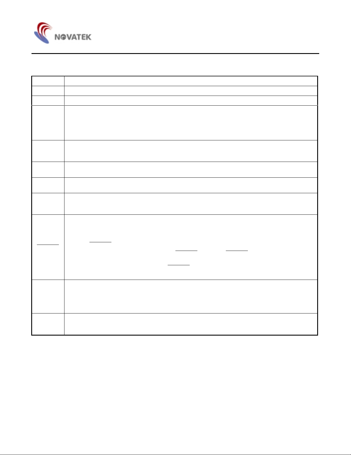
I/O
NT7704
DD
V
Input Signal
Control Signal
SS
V
DD
V
SS
V
SS
V
Output Signal
Control Signal
Applicable Pins
EIO1, EIO2
Control Signal 1
O
Control Signal 3
Input / Output Circuit
V0 V12
V43
SS
LCD Driver Output circuit
Control Signal 2
Control Signal 4
Applicable Pins
Y1 to Y240
V5V
5
Page 6
Pad Description
Segment mode
Symbol Function
V
DD
V
SS
VOR, V
V
, V
12R
V
, V
43R
V5R, V
D
0 - D7
XCK
LP
L/R
DISPOFF
FR
MD
Logic system power supply pin connects from +2.5 to +5.5V
Ground pin connects to 0V
Power supply pin for LCD driver voltage bias
OL
12L
43L
5L
Normally, the bias voltage used is set by a resistor divider
"
Ensure that the voltages are set such that V
"
To further reduce the differences betw een the output w aveforms of the LCD driver outpu t pins Y1 and Y
"
externally connect ViR and V
(I = 0, 12, 43, 5)
iL
SS
V
≤
Input pin for display data
In 4-bit parallel input mode, input data into the 4 pins D
"
In 8-bit parallel input mode, input data into the 8 pins D0 - D
"
Clock input pin for taking display data
Data is read on the falling edge of the clock pulse
"
Latch pulse input pin for display data
Data is latched on the falling edge of the clock pulse
"
Direction selection pin for reading display data
When set to VSS level "L", data is read sequentially from Y240 to Y1
"
When set to VDD level "H", data is read sequentially from Y1 to Y240
"
Control input pin for output deselect level
The input signal is lev el-shifted from the logi c volta ge level to the LCD driver voltage level, and contro ls the
"
LCD driver circuit.
When set to V
"
When DISPOFF is set to “L”, the contents of the line latch are reset, but the display data in the data
"
latch are read regardless of the condition of
the driver outputs deselect level (V
falling edge of the LP. At that time, if the
level “L”, the LCD driver output pins (Y1-Y240) are set to level V
SS
DISPOFF. When the DISPOFF function is canceled,
or V43), then outputs the contents of the date latch onto the next
12
DISPOFF removal time can not keep regulation with what is
shown on the AC characteristics, then it can not output the reading data correctly.
AC signal input for LCD driving waveform
The input signal is level-shifted from the logic voltage level to the driver voltage level and controls
"
the LCD driver circuit.
It normally inputs a frame inversion signal
"
The LCD driver output pin’s output voltage level can be set to the line latch output signal and the FR signal
Mode selection pin
When set to VSS level “L”, 8-bit paral lel input mode is set
"
When set to VDD level “H", 4-bit parallel input mode is set
"
NT7704
< V
< V
5
43
0 - D3
< V
12
0
. Connect D4 - D7 to VSS or V
5
240,
DD
6
Page 7
Segment mode continued
Symbol Function
Segment mode/common mode sele ctio n pin
When set to VDD level "H", segment mode is set
S/C
"
When set to V
"
level "L", common mode is set
SS
Input/output pin for chip selection
level “L”, EIO1 is set for output, and EIO2 is set for input
SS
XCK is “H” and then after 240-bits of data have been read,
EIO1, EIO
When L/R input is at V
"
When L/R input is at VDD level “H”, EIO1 is set for input, and EIO2 is set for output
"
2
During output, it is set to “H” while LP*
"
it is set to “L” for one cycle (from falling edge to falling edge of XCK), after which it returns to “H”
During input, after the LP signal is input, the chip is selected while EI is set to “L”. After 240-bits of
"
data have been read, the chip is deselected
LCD driver output pins
Y1 - Y
240
These correspond directly to each bit of the data latch, one level (V
output
Common mode
Symbol Function
NT7704
, V12, V43, or V5) is selected and
0
V
V
V0R, V
V
12R
V
43R
V5R, V
EIO
EIO
L/R
LP
DD
SS
, V
, V
1
2
0L
12L
43L
5L
Logic system power supply pin connects to +2.5 to +5.5V
Ground pin connects to 0V
Power supply pin for LCD driver voltage bias.
Normally, the bias voltage used is set by a resistor divider
"
< V
Ensure the voltages are set such that V
"
SS
V
≤
5 <V43
12
< V
0
To further reduce the differences between the output waveforms of the LCD driver output pins Y1 and
externally connect ViR and V
Y
240,
(I = 0, 12, 43, 5)
iL
Bi-directional shift register shift data input/output pin
Is an output pin when L/R is at V
"
When EIO
"
When EIO
"
is used as an input pin, it will be pulled-down
1
is used as an output pin, it won’t be pulled-down
1
level “L” and is an input pin when L/R is at VDD level “H”
SS
Bi-directional shift register shift data input/output pin
Is an input pin when L/R is at V
"
When EIO
"
When EIO
"
is used as an input pin, it will be pulled-down
2
is used as an output pin, it won’t be pulled-down
2
level “L” and is an output pin when L/R is at VDD level “H”
SS
Bi-directional shift register shift clock pulse input pin
Data is shifted on the falling edge of the clock pulse
"
Bi-directional shift register shift direction selection pin
Data is shifted from Y
"
set to V
level “H”
DD
to Y1 when it is set to VSS level “L”, and data i s shifted fr om Y1 to Y
240
when it is
240
7
Page 8
Common mode continued
Symbol Function
DISPOFF
Control input pin for output deselect level
The input signal is level-shifted from the logic voltage level to the LCD driver voltage level, and controls
"
the LCD driver circuit
When set to V
"
While set to “L”, the contents of the s hift resister are reset a nd are no t reading data. When the
"
level “L”, the LCD driver output pins (Y1-Y
SS
function is canceled, the driver o utputs des elect lev el (V
edge of the LP. At that time, if the
DISPOFF removal time can not keep regulation with w hat is shown on
the AC characteristics, the shift data is not read correctly
FR AC signal input for LCD driving waveform
The input signal is level-sh ifted from lo gic volta ge level t o the LCD driver v oltage lev el, and it control s the
"
LCD driver circuit
Normally, it inputs a frame inversion signal
"
The LCD driver output pin’s outp ut voltage level can be set using the shift reg ister output si gnal and the FR
signal
MD Mode selection pin
When set to V
"
level “L”, Single Mode operation is selected. When set to VDD level “H”, Dual Mode
SS
operation is selected
D
7
Dual Mode data input pin
According to the data shift direction of the data shift re gister, data can be input starting from t he 121st bit
"
When the chip is used in Dual Mode, D
When the chip is used in Single Mode, D
will be pulled-down
7
won’t be pulled-down
7
S/C Segment mode/common mode selectio n pin
When set to V
"
level “L”, common mode is set
SS
D0 - D6 Not used
Connect D
"
to VSS or VDD. Avoid floating
0-D6
XCK Not used
XCK is pull-down in common mode, so connect to V
"
Y1 - Y
240
LCD driver output pins
These correspond directly to each bit of the shift register, one level (V
"
output
) are set to level V
240
or V43), and the shift data is re ad on the falling
12
or leave open
SS
, V
0
5
, or V5) is selected and
12, V43
NT7704
DISPOFF
8
Page 9

Functional Description
1. Block description
1.1 Active Control
In segment mode, it controls the selection or deselection of
the chip. Following a LP signal input, and after the select
signal is input, a se lect signal is generated internally unti l 240
bits of data have been read in. Once data input has been
completed, a select signal for cascade connection is output,
and the chip is deselected.
In common mode, it controls the input/output data of the bidirectional pins.
1.2. SP Conversion & Data Control
In segment mode, it keeps input data which are 2 clocks of
XCK at 4-bit parallel mode into latch circuit, or keeps input
data which are 1 clock of XCK at 8-bit parallel mode into
latch circuit, after that they are put on t he i ntern al data bus 8
bits at a time.
1.3. Data Latch Control
In segment mode, it selec ts the state of the d ata latch, w hich
reads in the data bus signa ls. The sh ift dire ction i s contro lled
by the control logic and for every 16 bits of data read in, the
selection signal shifts one bit, based on the state of the
control circuit.
1.4. Data Latch
In segment mode, it latches the data on the data bus. The
latched state of each LCD driver output pin is controlled by
the control logic and the data latch control. 240 bits of data
are read in 20 sets of 8 bits.
NT7704
1.5. Line Latch/Shift Register
In segment mode, it ensures all 240 bits which have been
read into the data latch, are simult aneously latched on to the
falling edge of the LP signal, and output to the level shift
block.
In common mode, it shifts data from the data input pin on to
the falling edge of the LP signal.
1.6. Level Shifter
It ensures the logic voltage signal is level-shifted to the LCD
driver voltage level, and output to the driver block.
1.7. 4-Level Driver
It drives the LCD driver output pins from the line latch/shift
register data, selecting one of 4 levels (V
based on the S/C, FR and
1.8. Control Logic
Controls the operation of each block. In segment mode,
when an LP signal has been input, all blocks are reset and
the control logic waits f or the se lectio n sign al outpu t fro m the
active control block. Once the selection signal has been
output, operation of th e dat a l atc h and data transmission are
controlled, 240 bits of data are read in, and the chip is
deselected.
In common mode, it controls the direction of data shift.
DISPOFF signals.
, V12, V43, V5)
0
9
Page 10
NT7704
2. LCD Driver Output Voltage Level
The relationship between the data bus signal, AC converted signal FR and LCD driver output voltage is as shown in the table
below:
2.1. Segment Mode
1 - Y240
)
Here, V
SS
FR Latch Data
LLH V
LHH V
HLH V
HHH V
XXL V
< V
< V
V
≤
5
43
< V0, H: V
12
(+2.5 to +5.5V), L: V
DD
DISPOFF
SS
Driver Output Voltage Level (Y
43
5
12
0
5
(0V), X: Don't care
2.2. Common Mode
Here, V
SS
FR Latch Data
DISPOFF
LLH V
LHH V
HLH V
HHH V
XXL V
< V
< V
V
≤
5
43
< V0, H: V
12
(+2.5 to +5.5V), L: V
DD
(0V), X: Don't care
SS
Driver Output Voltage Level (Y
43
0
12
5
5
1 - Y240
)
Note: There are two kinds of power supply (logic level voltage, LCD driver voltage) for the LCD driver. Please supply regular
voltage which is assigned by specification for each power pin.
That time "Don't care" should be fixed to "H" or "L", avoiding floating.
10
Page 11
3. Relationship between the Display Data and Driver Output pins
3.1. Segment Mode:
(a) 4-bit Parallel Mode
NT7704
MD L/R EIO1EIO
H L Output Input
H H Input Output
(b) 8-bit Parallel Mode
MD L/R EIO1EIO
L L Output Input
L H Input Output
2
2
Data
Input
D
0
D
1
D
2
D
3
D
0
D
1
D
2
D
3
Data
Input
D
0
D
1
D
2
D
3
D
4
D
5
D
6
D
7
D
0
D
1
D
2
D
3
D
4
D
5
D
6
D
7
Number of Clock
60clock 59clock 58clcok ~ 3clock 2clock 1clock
Y1 Y5 Y9
Y2 Y6 Y10
Y3 Y7 Y11
Y4 Y8 Y12
Y240 Y236 Y232
Y239 Y235 Y231
Y238 Y234 Y230
Y237 Y233 Y229
~
~
~
~
~
~
~
~
Y229 Y233 Y237
Y230 Y234 Y238
Y231 Y235 Y239
Y232 Y236 Y240
Y12 Y8 Y4
Y11 Y7 Y3
Y10 Y6 Y2
Y9 Y5 Y1
Number of Clock
30clock 29clock 28clcok ~ 3clock 2clock 1clock
Y1 Y9 Y17 ~ Y217 Y225 Y233
Y2 Y10 Y18 ~ Y218 Y226 Y234
Y3 Y11 Y19 ~ Y219 Y227 Y235
Y4 Y12 Y20 ~ Y220 Y228 Y236
Y5 Y13 Y21 ~ Y221 Y229 Y237
Y6 Y14 Y22 ~ Y222 Y230 Y238
Y7 Y15 Y23 ~ Y223 Y231 Y239
Y8 Y16 Y24 ~ Y224 Y232 Y240
Y240 Y232 Y224 ~ Y24 Y16 Y8
Y239 Y231 Y223 ~ Y23 Y15 Y7
Y238 Y230 Y222 ~ Y22 Y14 Y6
Y237 Y229 Y221 ~ Y21 Y13 Y5
Y236 Y228 Y220 ~ Y20 Y12 Y4
Y235 Y227 Y219 ~ Y19 Y11 Y3
Y234 Y226 Y218 ~ Y18 Y10 Y2
Y233 Y225 Y217 ~ Y17 Y9 Y1
11
Page 12
3.2. Common Mode
NT7704
MD L/R Data Transfer Direction EIO
L
(Single)
L (shift to left) Y240 to Y1 Output Input X
H (shift to right) Y1 to Y240 Input Output X
L (shift to left)
H
(Dual)
H (shift to right)
Here, L: VSS (0V), H: V
(+2.5V to +5.5V), X: Don't care
DD
Note: "Don't care" should be fixed to "H" or "L", avoiding floating.
Y240 to Y121
Y120 to Y1
Y1 to Y120
Y121 to Y240
EIO
1
2
D
7
Output Input Input
Input Output Input
12
Page 13

4. Connection Examples of Segment Drivers
4.1. Case of L/R = “L”
NT7704
first data
XCK
LP
MD
FR
D0 - D7
V
SS
4.2. Case of L/R = “H”
(data taking flow)
XCKLPMD
FR
EIO1EIO2
L/R
D0 - D7
last data
Y240 ---------------------->Y1Y240 ----------------------->Y1 Y240 ---------------------->Y1
XCKLPMD
/8
FR
EIO1EIO2
L/R
D0 - D7
XCKLPMD
FR
EIO1EIO2
L/R
D0 - D7
V
DD
D0 - D7
FR
MD
LP
XCK
V
SS
/8
MD
LP
XCK
FR
D0 - D7
L/R
EIO1 EIO2
Y1 ---------------------->Y240
FR
D0 - D7
L/R
EIO1 EIO2
Y1 ---------------------->Y240 Y1 ---------------------->Y240
MD
LP
XCK
MD
LP
XCK
FR
D0 - D7
L/R
EIO1 EIO2
(data taking flow)
first data
last data
13
Page 14

5. Timing waveform of 4-Device cascade Connection of Segment Drivers
FR
LP
XCK
First data Last data
D0~D7
n12 n12 n12n12n12
device A device B device C device D
NT7704
EI
(device A)
EO
(device A)
EO
(device B)
EO
(device C)
H
L
n: 4-bit parallel mode 60
8-bit parallel mode 30
14
Page 15

6. Connection Examples for Common Drivers
NT7704
LP
V
SS (VDD
V
V
DISPOFF
CS
FR
SS
SS
First
Y240 Y1
D
LP
D7
MD
L/RFRDISPOFF
)
EIO1EIO2
CS
Y240 Y1
LP
D7
MD
L/RFRDISPOFF
EIO1EIO2
CS
Y240 Y1
LP
D7
MD
Last
EIO1EIO2
L/RFRDISPOFF
CS
Single Mode (Shifting towards the left)
FR
DISPOFF
V
DD
V
SS (VDD
V
LP
SS
)
FR
L/R
DISPOFF
D
EIO1 EIO2
MD
D7
FR
L/R
MD
DISPOFF
EIO1 EIO2
LP
Y240Y1
First
D7
Y240Y1
LP
FR
L/R
MD
D7
DISPOFF
EIO1 EIO2
Y240Y1
Last
LP
Single Mode (Sifting towards the right)
15
Page 16

NT7704
Last2First1 Last1 First2
D1
LP
D2
V
SS (VDD
V
DD
V
DISPOFF
FR
FR
DISPOFF
V
DD
V
DD
V
SS (VDD
D2
SS
Y240 Y1
EIO1EIO2
LP
D7
MD
L/RFRDISPOFF
Y240 Y1
Y121 Y120
EIO1EIO2
LP
D7
MD
L/RFRDISPOFF
Y240 Y1
EIO1EIO2
LP
D7
MD
L/RFRDISPOFF
)
Dual mode (Shifting towards the left)
)
LP
D1
FR
L/R
MD
D7
DISPOFF
EIO1 EIO2
Y240Y1
Dual mode (Shifting towards the right)
LP
FR
L/R
MD
D7
DISPOFF
EIO1 EIO2
Y240Y1 Y121Y120
16
LP
FR
L/R
MD
D7
DISPOFF
EIO1 EIO2
Y240Y1
Last2First1 Last1 First2
LP
Page 17

NT7704
7. Precaution
Be careful when connecting or disconnecting the power
This LSI has a high-voltage LCD driver, so it may be permanently damaged by a high current, which may occur if voltage is
supplied to the LCD driver power supply while the logic system power supply is floating.
The details are as follows:
When connecting the power supply, connect the LCD driver power after connecting the logic system power. Furthermore,
!
when disconnecting the power, disconnect the logic system power after disconnecting the LCD driver power.
We recommend that you connect a seri al re si stor ( 50-100 Ω) or fuse to the LCD dr iv er power V
!
limiting device. Also, set a suitable value of the resistor in consideration of LCD display grade.
In addition, when connecting the logic power supply, the logic condition of the LSI inside is insecure. Therefore, connect the
LCD driver power supply only after resetting the logic condition of this LSI inside to the
DISPOFF function. After that, the
DISPOFFcancel the function after the LCD driver power supply has become stable. Furthermore, when disconnecting the
power, set the LCD driv er output pins to level V
on the DISPOFF function. After that, disconnect the logic system pow er after
5
disconnecting the LCD driver power.
When connecting the power supply, follow the recommended sequence shown.
V
DD
V
DD
V
SS
V
DISPOFF
DD
V
SS
V
0
V
0
V
SS
of the system as a current
0
17
Page 18

NT7704
Absolute Maximum Rating*
DC Supply Voltage VDD . . . . . . . . . . . . . -0.3V to +7.0V
DC Supply Voltage V
Input Voltage . . . . . . . . . . . . . . . . . -0.3V to V
. . . . . . . . . . . . . . -0.3V to +30V
0
+0.3V
DD
Operating Ambient Temperature . . . . -30°C to +85°C
Storage Temperature . . . . . . . . . . . . .-45°C to +125°C
Electrical Characteristics
DC Characteristics
Segment Mode (V
Parameter Symbol Min. Typ. Max. Unit Condition
Operating Voltage 1 V
Operating Voltage 2 V
Input high voltage V
Input low voltage V
Output high voltage V
Output low voltage V
Input leakage current 1 I
= V5 = 0V, V
SS
= 2.5 - 5.5V, V0 = 15 to 30 V, and TA = -30 to +85°C, unless otherwise noted)
DD
DD
0
IH
IL
OH
OL
IH
2.5 - 5.5 V
15 - 30 V
0.8 V
DD
- - 0.2 V
V
- 0.4 - - V EIO1, EIO2 pins, I
DD
- - +0.4 V EIO1, EIO2 pins, I
--+1.0
*Comments
Stresses above those listed under "Absolute Maximum
Ratings" may cause permanent damage to this device.
These are stress ratings only. Functional operation of this
device under these or any other conditions above those
indicated in the operational sections of this specification is
not implied or intended. Exposure to the absolute maximum
rating conditions for extended periods may affect device
reliability.
--V
DD
D0 - 7, XCK, LP, L/R, FR, MD, S/C, EIO
EIO
V
D0 - 7, XCK, LP, L/R, FR, MD, S/C, EIO
A
µ
EIO
,
2
DISPOFF
,
2
DISPOFF
pins
= -0.4mA
OH
= +0.4mA
OL
pins, V
I
= V
DD
,
1
,
1
Input leakage current 2 I
IL
---1.0
A
µ
- 1.5 2.0 V0 = +30.0V
Output resistance R
ON
k
Ω
-2.02.5
Stand-by current I
Consumed current (1)
(Deselection)
Consumed current (2)
(Selection)
Consumed current I
I
DD1
I
DD2
SB
0
--10
A
µ
--2mAV
--12mAV
--1.5mAV
Note:
1. V
2. V
= +5.0V, V0 = +30V, VI = V
DD
= +5.0V, V0 = +30V, f
DD
SS
= 20MHz, No-load, EI = V
XCK
DD
The input data is turned over by the data taking clock (4-bit Parallel input mode)
3. V
= +5.0V, V0 = +30V, f
DD
= 20MHz, No-load. EI = V
XCK
SS
The input data is turned over by the data taking clock (4-bit parallel input mode)
4. V
= +5.0V, V0 = +30V, f
DD
= 20MHz, f
XCK
= 41.6kHz. f
LP
= 80 Hz, No-load
FR
The input data is turned over by the data taking clock (4-bit parallel-input mode)
D0 - 7, XCK, LP, L/R, FR, MD, S/C, EIO
EIO
,
2
DISPOFF
V0 = +20.0V
V
pin, Note 1
SS
pin, Note 2
DD
pin, Note 3
DD
pin, Note 4
0
pins, V
= V
I
Y
1 - Y240
V
∆
SS
= 0.5V
NO
pins,
,
1
18
Page 19

NT7704
Common Mode (V
= V5 = 0V, V
SS
Parameter Symbol Min. Typ. Max. Unit Condition
Operating Voltage V
Operating Voltage
Input high voltage V
Input low voltage V
Output high voltage V
Output low voltage V
Input leakage current 1 I
Input leakage current 2 I
Input pull down current I
Output resistance R
Stand-by current I
Consumed current (1) I
= 2.5 - 5.5V, V0 = 15 to 30 V, and TA = -30 to +85°C, unless otherwise noted)
DD
DD
V
0
IH
IL
OH
OL
IH
IL
PD
ON
SB
DD
2.5 - 5.5 V
15
0.8 V
DD
- - 0.2 V
V
- 0.4 - - V EIO1, EIO2 pins, I
DD
-30V
--V
DD
D0 - 7, XCK, LP, L/R, FR, MD, S/C, EIO
EIO
V
,
2
DISPOFF
- - +0.4 V EIO1, EIO2 pins, I
--+1.0
---1.0
- - 100
D0 - 6, LP, L/R, FR, MD, S/C and
A
µ
µ
µ
DISPOFF
D0 - 7, XCK, LP, L/R, FR, MD, S/C, EIO1,
A
EIO2,
DISPOFF
XCK, EIO1, EIO2, D7 pins
A
- 1.5 2.0 V0 = +30.0V
k
-2.02.5
--10
- - 120
Ω
A
µ
A
µ
V0 = +20.0V
V
pin, Note 1
SS
V
pin, Note 2
DD
pins, V
pins
= -0.4mA
OH
= +0.4mA
OL
= V
I
pins, V
DD
I
Y
1 - Y240
V
∆
= V
SS
pins,
= 0.5V
NO
,
1
Consumed current (2) I
Note:
1. V
2. V
= +5.0V, V0 = +30.0V, VI = V
DD
= +5.0V, V0 = +30.0V, f
DD
0
SS
= 41.6KHz, fFR = 80Hz, case of 1/480 duty operation, No-load
LP
- - 240
A
µ
V0 pin, Note 2
19
Page 20

AC Characteristics
NT7704
Segment Mode 1 (V
= V5 = 0V, V
SS
= 4.5 - 5.5V, V0 = 15 to 30V, and TA = -30 to +85°C, unless otherwise noted)
DD
Parameter Symbol Min. Typ. Max. Unit Condition
Shift clock period t
Shift clock "H" pulse width t
Shift clock "L" pulse width t
Data setup time t
Data hole time t
Latch pulse "H" pulse width t
Shift clock rise to Latch pulse rise time t
Shift clock fall to Latch pulse fall time t
Latch pulse rise to Shift clock rise time t
Latch pulse fall to Shift clock rise time t
Input signal rise time t
Input signal fall time t
Enable setup time t
DISPOFF
DISPOFF
Removal time
enable pulse width
WCK
WCKH
WCKL
DS
DH
WLPH
LD
SL
LS
LH
r
f
S
t
SD
t
WDL
50 - ns
15 - ns
15 - ns
10 - ns
12 - ns
15 - ns
0- ns
30 - ns
25 - ns
25 - ns
- 50 ns Note 2
- 50 ns Note 2
10 - ns
100 - ns
1.2 -
s
µ
tr, tf 10ns, Note 1
Output delay time (1) t
Output delay time (2) t
Output delay time (3) t
pd1
D
, t
pd3
Note:
1. Take the cascade connection into consideration.
2. (t
CK-tWCKII-twckl
)/2 is the maximum in the case of high speed operation.
pd2
- 30 ns CL = 15pF
-1.2
-1.2
µ
µ
s
s
CL = 15pF
CL = 15pF
20
Page 21

NT7704
Segment Mode 2 (V
= V5 = 0V, V
SS
= 3.0 - 4.5V, V0 = 15 to 30V, and TA = -30 to +85°C, unless otherwise noted)
DD
Parameter Symbol Min. Typ. Max. Unit Condition
Shift clock period t
Shift clock "H" pulse width t
Shift clock "L" pulse width t
Data setup time t
Data hole time t
Latch pulse "H" pulse width t
Shift clock rise to Latch pulse rise time t
Shift clock fall to Latch pulse fall time t
Latch pulse rise to Shift clock rise time t
Latch pulse fall to Shift clock fall time t
Input signal rise time t
Input signal fall time t
Enable setup time t
DISPOFF
DISPOFF
Removal time
enable pulse width
WCK
WCKH
WCKL
DS
DH
WLPH
LD
SL
LS
LH
r
f
S
t
SD
t
WDL
66 - ns
23 - ns
23 - ns
15 - ns
23 - ns
30 - ns
0- ns
50 - ns
30 - ns
30 - ns
- 50 ns Note 2
- 50 ns Note 2
15 - ns
100 - ns
1.2 -
s
µ
tr, tf 10ns, Note 1
Output delay time (1) t
Output delay time (2) t
Output delay time (3) t
pd1
D
, t
pd3
Note:
1. Take the cascade connection into consideration.
2. (t
CK-tWCKII-tWCKL
)/2 is the maximum in the case of high speed operation.
pd2
- 41 ns CL = 15pF
-1.2
-1.2
µ
µ
s
s
CL = 15pF
CL = 15pF
21
Page 22

NT7704
Segment Mode 3 (V
= V5 = 0V, V
SS
= 2.5 - 3.0V, V0 = 15 to 30V, and TA = -30 to +85°C, unless otherwise noted)
DD
Parameter Symbol Min. Typ. Max. Unit Condition
Shift clock period t
Shift clock "H" pulse width t
Shift clock "L" pulse width t
Data setup time t
Data hole time t
Latch pulse "H" pulse width t
Shift clock rise to Latch pulse rise time t
Shift clock fall to Latch pulse fall time t
Latch pulse rise to Shift clock rise time t
Latch pulse fall to Shift clock fall time t
Input signal rise time t
Input signal fall time t
Enable setup time t
DISPOFF
DISPOFF
Removal time
enable pulse width
WCK
WCKH
WCKL
DS
DH
WLPH
LD
SL
LS
LH
r
f
S
t
SD
t
WDL
82 - ns
28 - ns
28 - ns
20 - ns
23 - ns
30 - ns
0- ns
65 - ns
30 - ns
30 - ns
- 50 ns Note 2
- 50 ns Note 2
15 - ns
100 - ns
1.2 -
s
µ
tr, tf 10ns, Note 1
Output delay time (1) t
Output delay time (2) t
Output delay time (3) t
pd1
D
, t
pd3
Note:
1. Take the cascade connection into consideration.
2. (t
CK-tWCKII-tWCKL
)/2 is the maximum in the case of high speed operation.
pd2
- 57 ns CL = 15pF
-1.2
-1.2
µ
µ
s
s
CL = 15pF
CL = 15pF
22
Page 23

Timing waveform of the Segment Mode
NT7704
tWLPH
LP
XCK
D0 - D7
DISPOFF
LP
XCK
EI
tLD
tr tr
tWCK
LAST DATA TOP DATA
12
tS
tSL
tLS
tWDL tSD
tLH
tWCKH
tWCKL
tDS tDH
n
tD
EO
FR
LP
DISPOFF
Y1 - Y240
n: 4-bit parallel mode 60
8-bit parallel mode 30
tpd1
tpd2
tpd3
23
Page 24

NT7704
Common Mode (V
= V5 = 0V, V
SS
DD
Parameter Symbol Min. Typ. Max. Unit Condition
Shift clock period t
Shift clock "H" pulse width t
Data setup time t
Data hole time t
Input signal rise time t
Input signal fall time t
DISPOFF
DISPOFF
Removal time
enable pulse width
Output delay time (1) t
Output delay time (2) t
Output delay time (3) t
= 2.5 - 5.5V, V0 = 15 to 30V and TA = -30 to +85°C, unless otherwise noted)
t
, t
f
r
V
= +5.0V 10%
DD
= +2.5 - +4.5V
DD
CL = 15pF
CL = 15pF
WLPH
t
pd1
WLP
SU
H
r
f
t
SD
WDL
DL
, t
pd3
pd2
250 - - ns
15 - - ns
30 - - ns V
30 - - ns
50 - - ns
-50ns
-50ns
100 - - ns
1.2 - -
s
µ
- - 200 ns CL = 15pF
--1.2
--1.2
s
µ
s
µ
20ns
24
Page 25

Timing Characteristics of Common Mode
tr tf
LP
EIO2
(DI7)
EIO1
DISPOFF
FR
LP
tWLPH
tSU
NT7704
tWLP
tH
tDL
tWDL tSD
tpd1
tpd2
DISPOFF
Y1 - Y240
tpd3
25
Page 26

Application Circuit (for reference only)
960*480 DOT MATRIX
LCD PANEL
C
C
C
O
O
O
M
M
M
1
2
3
NT7704
SEG960
SEG959
Y1 - Y240
FR
LP
DISPOFF
XCK
Y1 - Y240
FR
LP
DISPOFF
XCK
Y1 - Y240
FR
LP
DISPOFF
XCK
SEG3
SEG2
SEG1
C
C
O
O
M
M
4
4
8
7
0
9
Y1 - Y240
FR
LP
DISPOFF
XCK
EIO1
D0 - D7
EIO2
EIO1
D0 - D7
EIO2
EIO1
D0 - D7
EIO2
EIO1
D0 - D7
EIO2
MD
S/C
L/R
MD
S/C
L/R
MD
S/C
L/R
MD
S/C
L/R
NT7704*4
/8
NT7704*2
V
0
V
0
Note: V0-V1>1.5V
Y1 - Y240
EIO1MDS/C
V
1
V
SS
Y1 - Y240
LP
FR
L/R
XCK
DISPOFF
D0 - D7
EIO2
EIO1MDS/C
LP
FR
L/R
XCK
DISPOFF
EIO2
D0 - D7
/5
/5
/8
LP
FR
V
V
2
V
3
4
YD
XCK
DISPOFF
7
- XD
0
XD
LCD controller
(n-4)R RR RR
V
V
5
DD
(case of 1/n bias)
V
SS
26
Page 27

Bonding Diagram
433
448
12968um
x
x
NT7704
ALK_L
x
1
( 0 , 0 )
Y
x
X
Dummy Pad
225432
208
Pad Location
Pad No. Designation X Y Pad No. Designation X Y
1V0L-6220 -521 31 V
2V0L-6150 -521 32 V
3V0L-6090 -521 33 V
4V0L-6030 -521 34 V
5V0L-5970 -521 35 V
6V0L-5910 -521 36 V
7V0L-5850 -521 37 V
8V0L-5790 -521 38 V
9V0L-5730 -521 39 V
10 V
11 V
12 V
13 V
14 V
15 V
16 V
17 V
18 V
19 V
20 V
21 V
22 V
23 V
24 V
25 V
26 V
27 V
28 V
29 V
30 V
0L
0L
0L
12L
12L
12L
12L
12L
12L
12L
12L
43L
43L
43L
43L
43L
43L
43L
43L
5L
5L
-5670 -521 40 V
-5610 -521 41 V
-5550 -521 42 V
-5490 -521 43 V
-5430 -521 44 V
-5370 -521 45 V
-5310 -521 46 V
-5250 -521 47 V
-5190 -521 48 V
-5130 -521 49 V
-5070 -521 50 V
-5010 -521 51 V
-4950 -521 52 V
-4890 -521 53 V
-4830 -521 54 V
-4770 -521 55 V
-4710 -521 56 V
-4650 -521 57 V
-4590 -521 58 V
-4530 -521 59 V
-4470 -521 60 V
5L
5L
5L
5L
5L
5L
5L
5L
5L
5L
SS
SS
SS
SS
SS
SS
SS
SS
SS
SS
SS
SS
SS
SS
SS
SS
SS
SS
SS
SS
-4410 -521
-4350 -521
-4290 -521
-4230 -521
-4170 -521
-4110 -521
-4050 -521
-3990 -521
-3930 -521
-3870 -521
-3810 -521
-3750 -521
-3690 -521
-3630 -521
-3570 -521
-3510 -521
-3450 -521
-3390 -521
-3330 -521
-3270 -521
-3210 -521
-3150 -521
-3090 -521
-3030 -521
-2970 -521
-2910 -521
-2850 -521
-2790 -521
-2730 -521
-2670 -521
NT7704
x
x
ALK_R
224
209
x
1168um
27
Page 28

NT7704
Pad Location
(continued)
Pad No. Designation X Y Pad No. Designation X Y
61 V
62 V
63 V
64 V
65 V
66 V
67 V
68 V
69 V
70 V
71 V
72 V
73 V
74 V
75 V
76 V
77 V
78 V
79 V
80 V
81 V
82 V
83 V
84 V
85 V
86 V
87 V
88 V
89 V
90 V
91 V
92 V
SS
SS
SS
SS
SS
SS
DD
DD
DD
DD
DD
DD
DD
DD
DD
DD
DD
DD
DD
DD
DD
DD
DD
DD
DD
DD
DD
DD
DD
DD
DD
DD
93 S/C -690 -521 133 EIO
-2610 -521 101 D1 -210 -521
-2550 -521 102 D1 -150 -521
-2490 -521 103 D1 -90 -521
-2430 -521 104 D2 -30 -521
-2370 -521 105 D2 30 -521
-2310 -521 106 D2 90 -521
-2250 -521 107 D3 150 -521
-2190 -521 108 D3 210 -521
-2130 -521 109 D3 270 -521
-2070 -521 110 D4 330 -521
-2010 -521 111 D4 390 -521
-1950 -521 112 D4 450 -521
-1890 -521 113 D5 510 -521
-1830 -521 114 D5 570 -521
-1770 -521 115 D5 630 -521
-1710 -521 116 D6 690 -521
-1650 -521 117 D6 750 -521
-1590 -521 118 D6 810 -521
-1530 -521 119 D7 870 -521
-1470 -521 120 D7 930 -521
-1410 -521 121 D7 990 -521
-1350 -521 122 XCK 1050 -521
-1290 -521 123 XCK 1110 -521
-1230 -521 124 XCK 1170 -521
-1170 -521 125
-1110 -521 126
-1050 -521 127
DISPOFF
DISPOFF
DISPOFF
1230 -521
1290 -521
1350 -521
-990 -521 128 LP 1410 -521
-930 -521 129 LP 1470 -521
-870 -521 130 LP 1530 -521
-810 -521 131 EIO
-750 -521 132 EIO
1
1
1
1590 -521
1650 -521
1710 -521
94 S/C -630 -521 134 FR 1770 -521
95 EIO
96 EIO
97 EIO
2
2
2
-570 -521 135 FR 1830 -521
-510 -521 136 FR 1890 -521
-450 -521 137 L/R 1950 -521
98 D0 -390 -521 139 L/R 2010 -521
99 D0 -330 -521 139 L/R 2070 -521
100 D0 -270 -521 140 MD 2130 -521
28
Page 29

NT7704
Pad Location
(continued)
Pad No. Designation X Y Pad No. Designation X Y
141 MD 2190 -521 181 V
142 MD 2250 -521 182 V
143 V
144 V
145 V
146 V
147 V
148 V
149 V
150 V
151 V
152 V
153 V
154 V
155 V
156 V
157 V
158 V
159 V
160 V
161 V
162 V
163 V
164 V
165 V
166 V
167 V
168 V
169 V
170 V
171 V
172 V
173 V
174 V
175 V
176 V
177 V
178 V
179 V
180 V
SS
SS
SS
SS
SS
SS
SS
SS
SS
SS
SS
SS
SS
SS
SS
SS
SS
SS
SS
SS
SS
SS
SS
SS
SS
SS
5R
5R
5R
5R
5R
5R
5R
5R
5R
5R
5R
5R
2310 -521 183 V
2370 -521 184 V
2430 -521 185 V
2490 -521 186 V
2550 -521 187 V
2610 -521 188 V
2670 -521 189 V
2730 -521 190 V
2790 -521 191 V
2850 -521 192 V
2910 -521 193 V
2970 -521 194 V
3030 -521 195 V
3090 -521 196 V
3150 -521 197 V
3210 -521 198 V
3270 -521 199 V
3330 -521 200 V
3390 -521 201 V
3450 -521 202 V
3510 -521 203 V
3570 -521 204 V
3630 -521 205 V
3690 -521 206 V
3750 -521 207 V
3810 -521 208 V
3870 -521 209 Y1 6430 -450
3930 -521 210 Y2 6430 -390
3990 -521 211 Y3 6430 -330
4050 -521 212 Y4 6430 -270
4110 -521 213 Y5 6430 -210
4170 -521 214 Y6 6430 -150
4230 -521 215 Y7 6430 -90
4290 -521 216 Y8 6430 -30
4350 -521 217 Y9 6430 30
4410 -521 218 Y10 6430 90
4470 -521 219 Y11 6430 150
4530 -521 220 Y12 6430 210
43R
43R
43R
43R
43R
43R
43R
43R
12R
12R
12R
12R
12R
12R
12R
12R
0R
0R
0R
0R
0R
0R
0R
0R
0R
0R
0R
0R
4590 -521
4650 -521
4710 -521
4770 -521
4830 -521
4890 -521
4950 -521
5010 -521
5070 -521
5130 -521
5190 -521
5250 -521
5310 -521
5370 -521
5430 -521
5490 -521
5550 -521
5610 -521
5670 -521
5730 -521
5790 -521
5850 -521
5910 -521
5970 -521
6030 -521
6090 -521
6150 -521
6220 -521
29
Page 30

NT7704
Pad Location
Pad No. Designation X Y Pad No. Designation X Y
221 Y13 6430 270 261 Y53 4050 529
222 Y14 6430 330 262 Y54 3990 529
223 Y15 6430 390 263 Y55 3930 529
224 Y16 6430 450 264 Y56 3870 529
225 Y17 6210 529 265 Y57 3810 529
226 Y18 6150 529 266 Y58 3750 529
227 Y19 6090 529 267 Y59 3690 529
228 Y20 6030 529 268 Y60 3630 529
229 Y21 5970 529 269 Y61 3570 529
230 Y22 5910 529 270 Y62 3510 529
231 Y23 5850 529 271 Y63 3450 529
232 Y24 5790 529 272 Y64 3390 529
233 Y25 5730 529 273 Y65 3330 529
234 Y26 5670 529 274 Y66 3270 529
235 Y27 5610 529 275 Y67 3210 529
236 Y28 5550 529 276 Y68 3150 529
237 Y29 5490 529 277 Y69 3090 529
238 Y30 5430 529 278 Y70 3030 529
239 Y31 5370 529 279 Y71 2970 529
240 Y32 5310 529 280 Y72 2910 529
241 Y33 5250 529 281 Y73 2850 529
242 Y34 5190 529 282 Y74 2790 529
243 Y35 5130 529 283 Y75 2730 529
244 Y36 5070 529 284 Y76 2670 529
245 Y37 5010 529 285 Y77 2610 529
246 Y38 4950 529 286 Y78 2550 529
247 Y39 4890 529 287 Y79 2490 529
248 Y40 4830 529 288 Y80 2430 529
249 Y41 4770 529 289 Y81 2370 529
250 Y42 4710 529 290 Y82 2310 529
251 Y43 4650 529 291 Y83 2250 529
252 Y44 4590 529 292 Y84 2190 529
253 Y45 4530 529 293 Y85 2130 529
254 Y46 4470 529 294 Y86 2070 529
255 Y47 4410 529 295 Y87 2010 529
256 Y48 4350 529 296 Y88 1950 529
257 Y49 4290 529 297 Y89 1890 529
258 Y50 4230 529 298 Y90 1830 529
259 Y51 4170 529 299 Y91 1770 529
260 Y52 4110 529 300 Y92 1710 529
(continued)
30
Page 31

NT7704
Pad Location
Pad No. Designation X Y Pad No. Designation X Y
301 Y93 1650 529 341 Y133 -750 529
302 Y94 1590 529 342 Y134 -810 529
303 Y95 1530 529 343 Y135 -870 529
304 Y96 1470 529 344 Y136 -930 529
305 Y97 1410 529 345 Y137 -990 529
306 Y98 1350 529 346 Y138 -1050 529
307 Y99 1290 529 347 Y139 -1110 529
308 Y100 1230 529 348 Y140 -1170 529
309 Y101 1170 529 349 Y141 -1230 529
310 Y102 1110 529 350 Y142 -1290 529
311 Y103 1050 529 351 Y143 -1350 529
312 Y104 990 529 352 Y144 -1410 529
313 Y105 930 529 353 Y145 -1470 529
314 Y106 870 529 354 Y146 -1530 529
315 Y107 810 529 355 Y147 -1590 529
316 Y108 750 529 356 Y148 -1650 529
317 Y109 690 529 357 Y149 -1710 529
318 Y110 630 529 358 Y150 -1770 529
319 Y111 570 529 359 Y151 -1830 529
320 Y112 510 529 360 Y152 -1890 529
321 Y113 450 529 361 Y153 -1950 529
322 Y114 390 529 362 Y154 -2010 529
323 Y115 330 529 363 Y155 -2070 529
324 Y116 270 529 364 Y156 -2130 529
325 Y117 210 529 365 Y157 -2190 529
326 Y118 150 529 366 Y158 -2250 529
327 Y119 90 529 367 Y159 -2310 529
328 Y120 30 529 368 Y160 -2370 529
329 Y121 -30 529 369 Y161 -2430 529
330 Y122 -90 529 370 Y162 -2490 529
331 Y123 -150 529 371 Y163 -2550 529
332 Y124 -210 529 372 Y164 -2610 529
333 Y125 -270 529 373 Y165 -2670 529
334 Y126 -330 529 374 Y166 -2730 529
335 Y127 -390 529 375 Y167 -2790 529
336 Y128 -450 529 376 Y168 -2850 529
337 Y129 -510 529 377 Y169 -2910 529
338 Y130 -570 529 378 Y170 -2970 529
339 Y131 -630 529 379 Y171 -3030 529
340 Y132 -690 529 380 Y172 -3090 529
(continued)
31
Page 32

NT7704
Pad Location
Pad No. Designation X Y Pad No. Designation X Y
381 Y173 -3150 529 416 Y208 -5250 529
382 Y174 -3210 529 417 Y209 -5310 529
383 Y175 -3270 529 418 Y210 -5370 529
384 Y176 -3330 529 419 Y211 -5430 529
385 Y177 -3390 529 420 Y212 -5490 529
386 Y178 -3450 529 421 Y213 -5550 529
387 Y179 -3510 529 422 Y214 -5610 529
388 Y180 -3570 529 423 Y215 -5670 529
389 Y181 -3630 529 424 Y216 -5730 529
390 Y182 -3690 529 425 Y217 -5790 529
391 Y183 -3750 529 426 Y218 -5850 529
392 Y184 -3810 529 427 Y219 -5910 529
393 Y185 -3870 529 428 Y220 -5970 529
394 Y186 -3930 529 429 Y221 -6030 529
395 Y187 -3990 529 430 Y222 -6090 529
396 Y188 -4050 529 431 Y223 -6150 529
397 Y189 -4110 529 432 Y224 -6210 529
398 Y190 -4170 529 433 Y225 -6430 450
399 Y191 -4230 529 434 Y226 -6430 390
400 Y192 -4290 529 435 Y227 -6430 330
401 Y193 -4350 529 436 Y228 -6430 270
402 Y194 -4410 529 437 Y229 -6430 210
403 Y195 -4470 529 438 Y230 -6430 150
404 Y196 -4530 529 439 Y231 -6430 90
405 Y197 -4590 529 440 Y232 -6430 30
406 Y198 -4650 529 441 Y233 -6430 -30
407 Y199 -4710 529 442 Y234 -6430 -90
408 Y200 -4770 529 443 Y235 -6430 -150
409 Y201 -4830 529 444 Y236 -6430 -210
410 Y202 -4890 529 445 Y237 -6430 -270
411 Y203 -4950 529 446 Y238 -6430 -330
412 Y204 -5010 529 447 Y239 -6430 -390
413 Y205 -5070 529 448 Y240 -6430 -450
414 Y206 -5130 529 ALK_L -6318 -533
415 Y207 -5190 529 ALK_R 6318 -533
(continued)
32
Page 33

Dummy Pad Location (Total: 6 pin)
NO. X Y NO. X Y
1 6430 -520 4 -6280 529
2 6430 520 5 -6430 520
6280 529
3
-6430 -520
6
NT7704
33
Page 34

Package Information
A1A2D1
C1
D1
D2
16n1m1
D1
C1
r r
n1
m1
m2
H
J
B
C3
65m1n2 (L) 65m1n2 (R)
D1
NT7704
m1
n2
NT7704
A1
D1
208m1n1
n1
m1
m3
76m3n2
D2
n1
m2
4n1m2
m2
n1
2m2n1
D2
C2
m3
m1
n2
D2
m2
m2
C3
D1
A2
C1
D1
D2
16n1m1
n1
m1
D1
C1
H
J
B
Chip Outline Dimensions
unit: um
Symbol Dimensions in um Symbol Dimensions in um
A1 204 H 51
A2 54 J 166
B 264 m1 39
C1 64 m2 55
C2 55 m3 38
C3 63 n1 72
D1 70 n2 90
D2 60 r 35
34
Page 35

TCP Pin Layout
DUMMY
Y1
Y2
Y5
Y118
Y119
Y120
Y121
Y122
Y123
NT7704
33
34
Y3
35
36
Y4
37
DUMMY
V0R
32
V0R
31
30
V12R
V43R
29
V5R
28
NC
27
VSS
26
NC
25
MD
24
L/R
23
FR
22
EIO1
21
LP
20
DISPOFF
150
151
152
153
154
155
NT7704
19
XCK
18
17
D7
16
D6
15
D5
14
D4
13
D3
12
D2
11
D1
10
D0
9
EIO2
8
S/C
7
VDD
6
VSS
5
V5L
4
V43L
3
V12L
2
V0L
V0L
1
DUMMY
Y236
Y237
Y238
Y239
Y240
DUMMY
268
269
270
271
272
(COPPER SIDE VIEW)
35
Page 36

External View of TCP Pins
NT7704
NT7704H - TABF4
36
Page 37

NT7704
Cautions concerning storage:
1. When storing the product, it is recommended that it be left in its shipping package.
After the seal of the packing bag has been broke, store the products in a nitrogen atmosphere.
2. Storage conditions :
Storage state Storage conditions
unopened
After seal of broken
3. Don't store in a location exposed to corrosive gas or excessive dust.
4. Don't store in a location exposed to direct sunlight of subject to sharp changes in temperature.
5. Don't store the product such that it is subjected to an excessive load weight, such as by stacking.
6. Deterioration of the plating may occur after long-t erm storage, so special care is required.
It is recommended that the products be inspected before use.
(less than 90 days)
(less than 30 days)
Temperature: 5 to 30; humidity: 80%RH or less
Room temperature, dry nitrogen atmosphere
37
Page 38

Tray Information
NT7704
f
e
4
25=100
H30-523
59-25
c
W2
W1
T1T2
SECTION Y-Y
XX
YY
W1
g
h
a
W2
b
T2
T1
e
f
d
g
h
SECTION X-X
Tray Outline Dimensions unit: mm
Symbol Dimensio ns in mm Symbol Dimensions in mm
a 1.30 g 0.64
b 2.67 h 4.20
c 13.30 W1 76.0
d 16.26 W2 68.0
e 1.60 T1 71.0
f 1.40 T2 68.3
38
Page 39

Ordering Information
Part No. Package
NT7704H-BDT Au bump on chip tray
NT7704H-TABF4 TCP Form
NT7704
39
Page 40

Product Spec. Change Notice
Version Content Date
1.0 TCP and tray information addition (Page 36-39) Dec. 2001
0.2
0.1 Pad Location Addition Nov. 2000
0.0 Original Nov. 2000
Gold Bump Size revision (Page 34)
m1: 45 → 39, m2: 58 → 55
NT7704
NT7704 Specification Revision History
Sep. 2001
40
 Loading...