

Page 1
Features
NT6868C
Keyboard Controller
n Built-in 6502 8-bit CPU
n 2 MHz CPU operation frequency
n 4K bytes of ROM
n 128 bytes of SRAM
n One 8-bit programmable base timer with 1 - 256 µsec
interval
n 29 programmable bi-directional I/O pins
n 3 LED direct sink pins with internal serial resistors
n Mask optional for built-in RC oscillator with an
external resistor or external ceramic resonator
applied
n Mask optional for DATA/CLK driving capability
n Watch-dog timer
n Built-in power-on reset
n Built-in low voltage reset
n CMOS technology for low power consumption
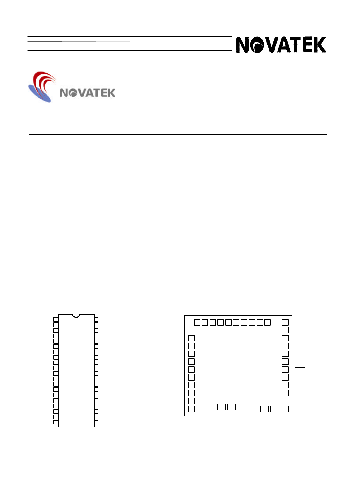
n Available in 40 pin DIP package and 40 pad CHIP
FORM
General Description
NT6868C is a single chip micro-controller for keyboard
applications. It incorporates a 6502 8-bit CPU core, 4K
bytes of ROM and 128 bytes of RAM used as working
RAM and stack area. It also includes 29 programmable
bi-directional I/O pins and one 8-bit pre-loadable base
timer.
Additionally, it includes a built-in low voltage reset, a
4MHz RC oscillator that only requires an externally
applied or a 4MHz ceramic resonator, and a watch-dog
timer that has a resistor preventing system standstill.
Pin Configuration Pad Configuration
P
P
P
P
1
1
5
4
R
V
D
/
D
O
S
C
O
P
1
3
NT6868CH
40393837
O
S
C
I
GND
NC
DATA
CLK
P30
P31
P32
P33
P34
RESET
P00
P01
P02
P03
P05
P06
P07
P10
P11
1
2
3
4
5
6
7
8
NT6868C
9
10
11
12
13
14
15
16 25
17
18
19
20
1
1
7
6
OSCI
40
R/OSCO
39
V
DD
38
LED2
37
LED1
36
LED0
35
P27
34
P26
33
P25
32
31
P24
P23
30
P22
29
P21
28
27
P20
P17P04
26
P16
24
P15
23
P14
22
P13
P12
21
P20
P21
P22
P23
P24
P25
P26
P27
LED0
LED1
26 25 24 23 22 21 20 19 18 17
27
28
29
30
31
32
33
34
35
36
L
E
D
2
P
P
P
P
1
0
NCD
P
0
0
7
6
16
P05
15
P04
14
P03
13
P02
12
P01
11
P00
10
RESET
9
P34
8
P33
7
P32
P31
6 5 4 3 2
C
P
A
L
3
T
K
0
A
1
1
2
1
1
G
N
D
1 V2.0
Page 2
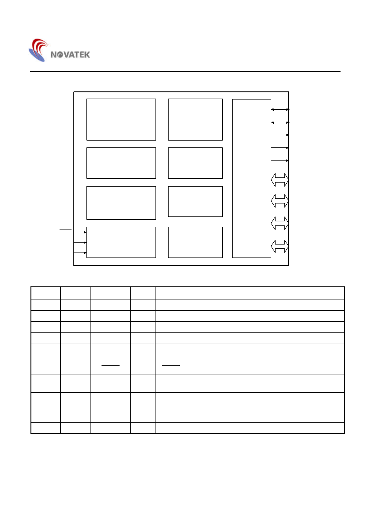
Block Diagram
TIMING GENERATOR
(RC OSC/Ceramic Resonator: 4MHz)
4K BYTES
ROM
NT6868C
CLK
DATA
LED0
LED1
128 BYTES
SRAM + STACK
WATCH DOG
TIMER
BASE TIMER
I/O PORTS
RESET
VDD
GND
6502
CPU
INT. CONTROLLER
POWER-ON RESET/
LOW VOLTAGE RESET
Pin and Pad Descriptions
Pin No. Pad No. Designation I/O Description
1 1 GND P Ground pin
2 2 NC - No connection, recommended to connect V DD or floating
3 3 DATA I/O I/O, 10KΩ pull-up resistor for communication
4 4 CLK I/O I/O, 10KΩ pull-up resistor for communication
LED2
P00 - P07
P10 - P17
P20 - P27
P30 - P34
5 - 9,
11 - 34
10 10
35 - 37 35 - 37 LED0 -
5 - 9,
11 - 34
P30 - P34,
P00 - P27
RESET
I/O Bi-directional I/O pins
I
RESET signal input pin with internal pull-up resistor; Active low
O LED direct sink pins
LED2
38 38
V
DD
P Power supply
39 39 R/OSCO I 47KΩ resistor connected for RC OSC or 4MHz ceramic resonator
connection
40 40 OSCI - No connection for RC OSC connection; for 4MHz ceramic resonator
* Under the constraint of the maximum frequency variation, (∆F/F)
be selected while pins 39 and 40 are connected to a ceramic resonator. If (∆F/F)
, ≤ ±1%, code 3, 7 (ceramic resonator option) must
max
, ≤ ±10%, code 1, 5 (RC OSC option),
max
then it is recommended to be selected. Also, connect pin 39 a 47KΩ resistor with, ≤ ±1% accuracy to V DD while pin 40 is
floating.
2
Page 3
Functional Description
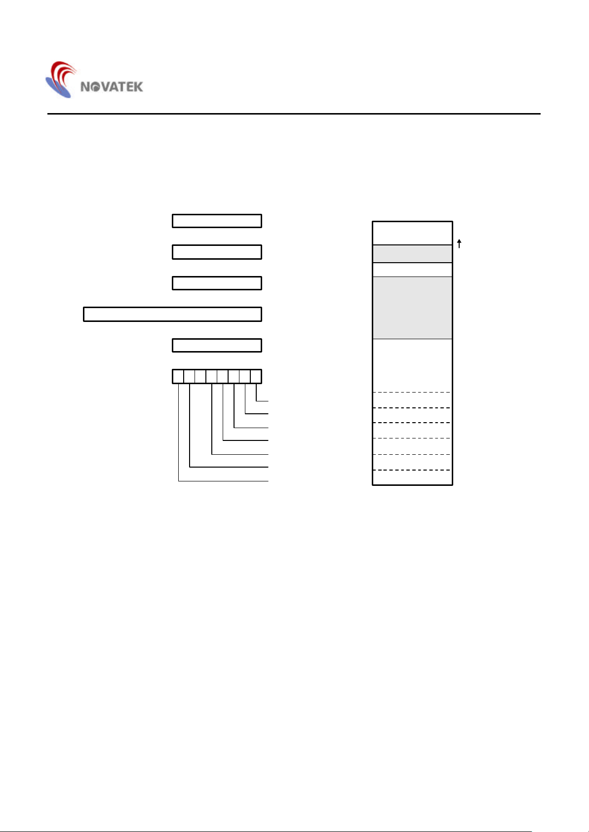
6502 CPU
6502 is an 8-bit CPU. Please refer to 6502 data sheet for more details.
7 0
ACCUMULATOR A
7 0
INDEX REGISTER X
7 0
INDEX REGISTER Y
0000
009F
00C0
00CF
SRAM
UNUSED
SYSTEM REGISTERS
NT6868C
STACK PTR
15 0
PROGRAM COUNTER PC
7 0
S
7 0
S V B D I Z C
STACK POINTER SP
STATUS REGISTER P
CARRY
ZERO
INTERRUPT MASK
DECIMAL MODE
BREAK
OVERFOLW
SIGN
EC00
FFFA
FFFB
FFFC
FFFD
FFFE
FFFF
UNUSED
USER ROM
NMI-L
NMI-H
RST-L
RST-H
IRQ-L
IRQ-H
Figure 1. 6502 CPU Registers and Status Flags Figure 2. NT6868C Memory Map
NMI VECTOR
IRQ VECTOR
3
Page 4
NT6868C
System Reserved Registers
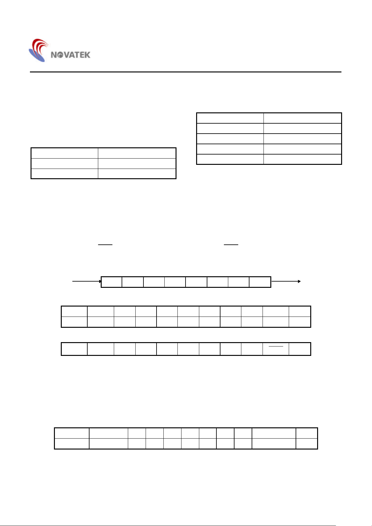
Address Register Bit7 Bit6 Bit5 Bit4 Bit3 Bit2 Bit1 Bit0 R/W
$00C0 BT BT7 BT6 BT5 BT4 BT3 BT2 BT1 BT0 W
$00C1 TCON - - - - - - -
$00C2 CLRIRQX - - - - - - - CLRIRQTMR W
$00C3 PORT0 PD07 PD06 PD05 PD04 PD03 PD02 PD01 PD00 RW
$00C4 PORT1 PD17 PD16 PD15 PD14 PD13 PD12 PD11 PD10 RW
$00C5 PORT2 PD27 PD26 PD25 PD24 PD23 PD22 PD21 PD20 RW
$00C6 PORT3 - - - PD34 PD33 PD32 PD31 PD30 RW
$00C7 CLK - - - - - - - CLK RW
$00C8 DATA - - - - - - - DATA RW
$00C9 LED - - - - - LED2 LED1 LED0 W
$00CA CLRWDT 0 1 0 1 0 1 0 1 W
$00CB X X X X X X X X X X
$00CC X X X X X X X X X X
$00CD X X X X X X X X X X
$00CE X X X X X X X X X X
$00CF X X X X X X X X X X
- : no effect X : access not allowed
ENBT
W
4K X 8 ROM
The built-in ROM program code, executed by the 6502
CPU, has a capacity of 4K X 8 bits and is addressed
from F000H to FFFFH.
128 X 8 SRAM
The built-in SRAM is used for general purpose data
memory and for the stack area. SRAM is addressed from
0000H to 007FH. The user can allocate stack area in the
SRAM by setting the stack pointer register (S). Since
6502C’s default stack pointer is 01FFH, it must be
mapped to 007FH. Mapping from 01XX to 00XX is done
internally by setting the S register to 7FH via software
programming.
For example :
LDX #$7F
TXS
Power-On Reset
The built-in power-on reset circuit can generate a 150ms
pulse to reset the entire chip. The beginning of the
150ms pulse occurs at 60% of VDD when powered on.
power
VDD
60%
The start of 150ms pulse
t
4
Page 5
Timing Generation
NT6868C
This block generates the system timing and control
signal supplied to the CPU and on-chip peripherals.
There are two types of system clock sources: a built-in
RC oscillator or an external ceramic resonator. Both of
them are mask optional and generate a 4MHz system
clock. They also generate 2MHz for the CPU, and 1 MHz
for the base timer. The following shows the relationship
of code type number with oscillation type.
Oscillator Code Number
RC OSC 1, 5
External Resistor 3, 7
The following table provides the relationship between
the external resistor and the RC OSC frequency. (This is
for reference only)
External Resistor (KΩ) RC OSC Frequency (MHz)
39 4.7
43 4.44
47 4
56 3.68
Base Timer
The base timer is an 8-bit counter with a 1MHz clock source. The base timer can be enabled/disabled by the CPU. After a
reset, the base timer is disabled and cleared. The base timer can be preset by writing BT7 - BT0 to the BT register at any
time. When enabled, the base timer starts counting from the preset value. When the value reaches FFH, it generates a
timer interrupt only if the timer interrupt is enabled. When it reaches the maximum value of FFH, the base timer will wrap
around and begin counting at 00H. The timer interval can be programmed from 1 - 256 µsec. The base timer can be
enabled by writing a '0' to 'ENBT' in the TCON (Timer Control) register. The ENBT is a level trigger.
Base timer structure:
8-Bit timer
1µs
BT Pre-loaded Data:
Addr. Bit 7 6 5 4 3 2 1 0 R/W
$00C0 BT BT7 BT6 BT5 BT4 BT3 BT2 BT1 BT0 (W)
Timer Control Register:
$00C1 TCON - - - - - - -
BT7 BT6 BT5 BT4 BT2 BT2 BT1 BT0
ENBT
TMRINT
(W)
INT. Controller
When a BASE TIMER overflow occurs, it will set the IRQTMR flag. The IRQTMR flag cannot be directly accessed by the
software. Once set by an interrupt source, it remains HIGH unless cleared by writing '1' to the corresponding bit in
CLRIRQX ($00C2H). This register is cleared to '0' on initialization by a system reset.
When an interrupt occurs, the CPU will jump to $FFFEH & $FFFFH to execute the interrupt service routine. When a BASE
TIMER interrupt occurs and enters the interrupt service routine, the IRQTMR flag must be cleared by the software.
Interrupt Control Register:
Addr. Bit 7 6 5 4 3 2 1 0 R/W
$00C2 CLRIRQX - - - - - - - CLRIRQTMR (W)
5
Page 6

NT6868C
I/O Ports
The NT6868C has 31 pins dedicated to input and output. These pins are grouped into 6 ports as follows:
PORT 0 (P00 - P07):
Port 0 is an 8-bit bi-directional CMOS I/O port that is internally pulled HIGH by PMOS. Each pin of port 0 can be bit
programmed as an input or output pin under the software control. When programmed as output, data is latched to the port
data register and output to the pin. Port 0 pins with ''1'' written to them are pulled HIGH by the internal PMOS pull-ups, and
are used as input in that state. These input signals can then be read. The port output will be HIGH after reset.
PORT 1 ( P10 - P17 ) : These functions are the same as PORT 0.
PORT 2 ( P20 - P27) : These functions s are the same as PORT 0.
PORT 3 ( P30 - P34) : These functions are the same as PORT 0.
CLK & DATA : These two pins have the same structure as I/O ports.
PORT Registers:
Addr. Bit 7 6 5 4 3 2 1 0 R/W
$00C3 PORT0 PD07 PD06 PD05 PD04 PD03 PD02 PD01 PD00 (RW)
$00C4 PORT1 PD17 PD16 PD15 PD14 PD13 PD12 PD11 PD10 (RW)
$00C5 PORT2 PD27 PD26 PD25 PD24 PD23 PD22 PD21 PD20 (RW)
$00C6 PORT3 - - - PD34 PD33 PD32 PD31 PD30 (RW)
$00C7 CLK - - - - - - - CLK (RW)
$00C8 DATA - - - - - - - DATA (RW)
WREN
DB
RST
RDENB
Latch
L
Q
D
SD
IO Port Structure
VDD
Weak PMOS
IO
6
Page 7

NT6868C
LED Port
There are 3 LED direct sink pins which require no external serial resistors. The address is mapped to address $00C9.
Addr. Bit 7 6 5 4 3 2 1 0 R/W
$00C9 LED - - - - - LED2 LED1 LED0 (W)
WREN
DB
RST
LED [ 0 ]
L
Q
D
SD
WREN
DB
RST
L
Q
D
SD
VDD
LED [ 1:2 ]
LED0 Port Structure LED1, LED2 Port Structures
Watch-Dog Timer
NT6868C implements a watch-dog timer, which protects programs against system standstill. The clock of the watch-dog
timer is derived from the on-chip RC oscillator. The watch-dog timer interval is about 0.175 of a second. The timer must
be cleared within every 0.175 second during normal operation; otherwise, it will overflow and cause a system reset. The
watch-dog timer is cleared and enabled after a system reset. It cannot be disabled by the software. The user can clear the
watch-dog timer by writing #55H to CLRWDT ($00CAH) register.
For example:
LDA #$55
STA $00CA
Addr. Bit 7 6 5 4 3 2 1 0 R/W
$00CA CLRWDT 0 1 0 1 0 1 0 1 (W)
Low Voltage Reset (LVR) Circuit
The NT6868C will check on the voltage level of the power supply. When the voltage level of power supply is below a
threshold of 3.0V (Typical), the LVRC will issue a reset output to the chip until the power voltage level is above a threshold
voltage of 3.0V (Typical) again. As soon as the power voltage reaches 3.0V (Typical), the entire chip will be reset for about
150ms.
RESET
NT6868C can also be externally reset through the RESET pin. A reset is initiated when the signal at the RESET pin is
held LOW for at least 10 system clocks. As soon as the RESET signal goes high, the NT6868C begins to reset for about
150ms. The following shows the definition of the RESET input at LOW pulse width.
VDD
20%VDD 20%VDD
Trstb
VDD
7
Page 8

NT6868C
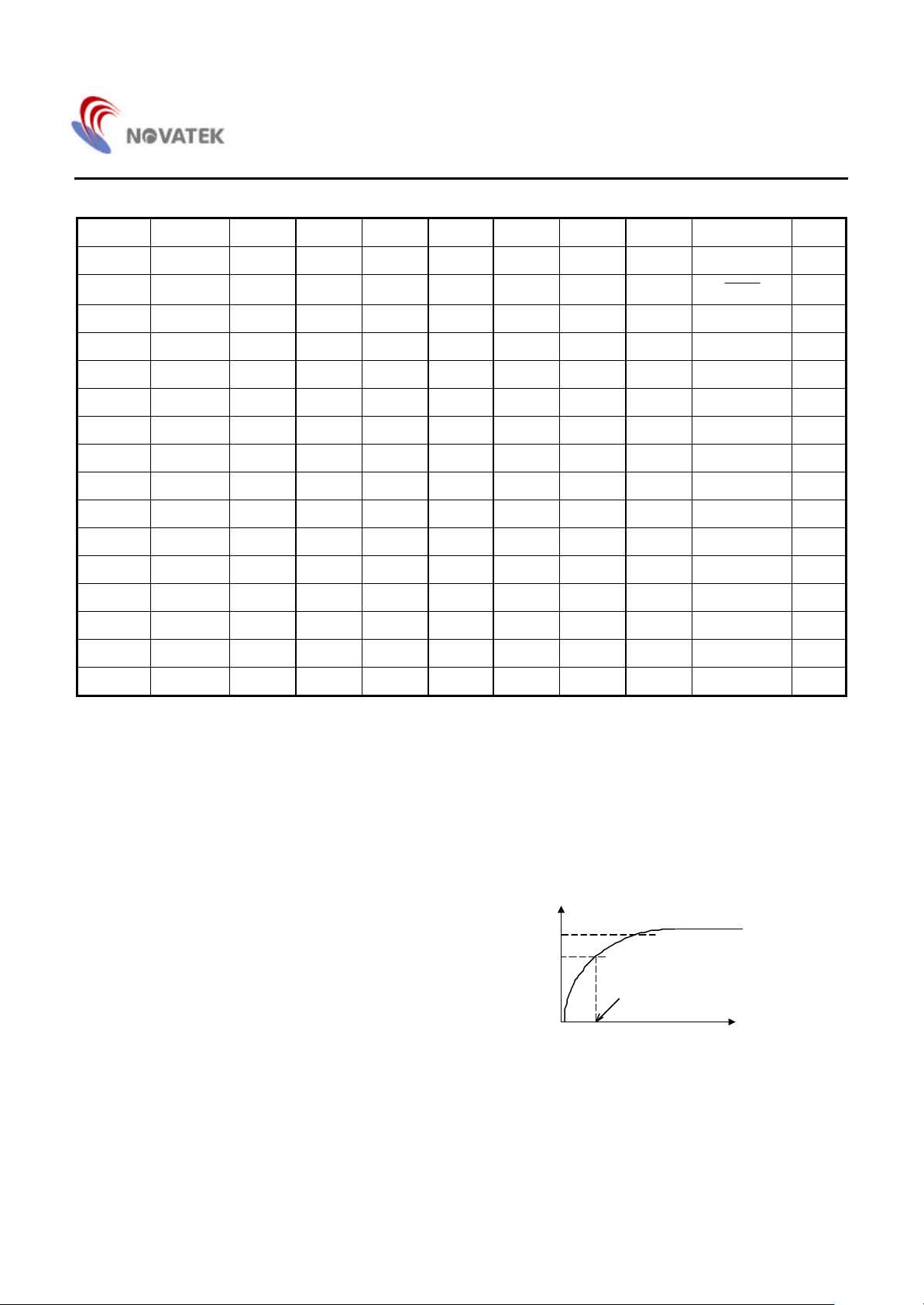
Absolute Maximum Ratings*
DC Supply Voltage . . . . . . . . . . . . . . -0.3V to +7.0V
*Comments
Stresses above those listed under "Absolute Maximum
Ratings" may cause permanent damage to this device.
Input/Output Voltage . . . . . . GND -0.2V to VDD + 0.2V
Operating Ambient Temperature . . . . . . 0° C to +70°C
Storage Temperature . . . . . . . . . . . . . -55 °C to +125°C
Operating Voltage (VDD) . . . . . . . . . .+4.5V to 5.5V
DC Electrical Characteristics (V
= 5V, GND = 0V, TA = 25°C, F
DD
These are stress ratings only. Functional operation of
this device at these or any other conditions above those
indicated in the operational sections of this specification
is not implied or intended. Exposure to the absolute
maximum rating conditions for extended periods may
affect device reliability.
= 4MHz, unless otherwise specified)
OSC
Symbol Parameter Min. Typ. Max. Unit Conditions
I
CC
V
IH
V
IL
V
OH1
V
OH2
Power Supply Current 20 mA No load
Input High Voltage 2 V
Input Low Voltage 0.8 V
Output High Voltage (Port 0, 1, 2, 3) 2.4 V
Output High Voltage (CLK, DATA) 2.4 V
IOH = -100µA
IOH = -400µA, Note 1
V
OH3
V
OL1
V
OL2
V
OL3
Output High Voltage (CLK, DATA) 2.4 V
Output Low Voltage (PORT 0, 1, 2) 0.4 V
Output Low Voltage (PORT 3) 0.4 V
Output Low Voltage (CLK, DATA) 0.4 V
IOH = -800µA, Note 2
IOL = 4mA
IOL = 5mA
IOL = 10mA
∆F/F Initial Frequency Variation 1 +/-10 % For RC OSC option
only; By Lots
∆F/F Frequency Variation 2 +/-1 % For ceramic resonator
option only; By Lots
I
LED
V
LVR
T
POR
T
RSTB RESET Input Low Pulse Width
R
PH RESET Pull High Resistor
LED Sink Current (LED 0, 1, 2) 10 14 17 mA
Low Voltage Reset Threshold 3.0 V
Power-on Reset Time 120 150 180 ms
2.5 µs 10 system clocks
220 KΩ
VOL = 3.2V
Note 1: There are 2 types of DATA/CLK driving capabilities. This condition of VOH2 is the same as the specification of
NT6868A. Under this condition, the user can select mask option 1 or 3.
Note 2: The driving capability of DATA/CLK is higher than V
. Under this condition, the user can select mask option 5 or
OH2
7.
8
Page 9

Application Circuit I (for reference only)
NT6868C
VDD
4.7 - 10 mf
P00
VDD
Esc
(K45)
Macro
F4
G
H
F6
"
'
(L)
Alt
F11
Space
0
Ins
.
Del
GND
LED0
LED1
LED2
RESET
DATA
CLK
R/OSCO
Ctrl
|
\(K42)
Enter
Num
Lock
/
Scroll Lock
Num Lock
Caps Lock
0.1mf
47K (System clock can be decreased
by increasing the resistance)
(R)
Z
K131
X
K132
C
K133
V
B
M
N
<
,
K56
>
.
APP
?
/
(R)
Alt
F12
*
-
P01
P02
P03
P04
P05
P06
P07
P10
P11
P12
P13
P14
P15
P16
P17
P30
NT6868C
P31
P20
P21
P22
P23
P24
P25
P26
P27
R0 R1 R2 R3 R4 R5 R6 R7
S0
Pause
S1
S2
S3
S4
S5
S6
S7
S8
S9
S10
S11
S12
S13
S14
S15
S16
S17
Q
W
R
U
O
Scroll
Lock
K14
7
Home
8
9
PgUp
Tab
E
I
P
Back
Space
+
K107
(L)
Shift
WINL
Caps
Lock
F3
F7
4
5
6
A
S
D
T
F
Y
J
}
]
K
L
{
:
[
;
|
\(K29)
1
End
2
3
PgDn
(R)
Enter
(R)
Shift
WINR
VDD
(L)
Ctrl
~
,
F1
F2
%
5
^
6
+
=
F8
-
F9
Delete
Insert
Page
Up
Home
VDD
Optional
KBD DATA
KBD CLOCK
Print
Screen
Page
Down
End
F5
F10
!
1
@
2
#
3
$
4
&
7
*
8
(
9
)
0
9
Page 10

Application Circuit II (for reference only)
P00
P01
P02
P03
P04
P05
P06
P07
P10
P11
P12
P13
P14
P15
P16
P17
P30
P31
P20
P21
P22
P23
P24
P25
P26
P27
VDD
VDD
NT6868C
4.7 - 10µf
GND
LED0
LED1
LED2
RESET
DATA
CLK
R/OSCO
OSCI
Scroll Lock
Num Lock
Caps Lock
0.1µf
4MHz
Ceramic Resonator
VDD
Optional
NT6868C
KBD
DATA
KBD
CLOCK
R0 R1 R2 R3 R4 R5 R6 R7
Esc
(K45)
F4
G
H
F6
"
'
(L)
Alt
F11
Space
Del
|
/
\(K42)
Num
Lock
(R)
Ctrl
Z
X
C
V
M
<
,
>
.
Enter
*
K131
K132
K133
B
N
K56
APP
?
(R)
Alt
F12
/
-
S0
S1
S2
S3
S4
S5
S6
S7
S8
S9
S10
S11
S12
S13
S14
S15
S16
S17
Pause
Q
W
E
R
U
O
P
Scroll
Lock
K14
7
Home
8
9
PgUp
Tab
Caps
Lock
I
Back
Space
4
5
6
+
K107
(L)
Shift
WINL
A
S
Macro
D
F3
F
T
J
Y
}
K
]
L
F7
:
{
;
[
|
\(K29)
1
End
2
0
Ins
3
.
PgDn
(R)
Enter
(R)
Shift
WINR
Delete
Insert
Page
Up
Home
(L)
Ctrl
F1
~
,
F2
%
5
^ &
6
+
=
F8
-
F9
Print
Screen
Page
Down
End
F5
@
F10
!
1
2
#
3
$
4
7
*
8
(
9
)
0
10
Page 11

Application Circuit For Windows 2000 Standard Code
S0
S1
S2
S3
S4
S5
S6
S7
S8
S9
S10
S11
S12
S13
S14
S15
S16
S17
P15
P30
P31
P00
P01
P02
P03
P04
P13
P14
P12
P10
P07
P06
P05
P11
P16
P17
P32S18
NT6868A/C
R_OSC
LED 0
LED 1
LED 2
VDD
GND
NT6868C
47K
Scroll Lock
.1uF
Num Lock
Caps Lock
VDD
10uF
GND
R0
R1
R2
R3
R4
R5
R6
R7
P20
P21
P22
P23
P24
P25
P26
P27
11
DATA
CLOCK
RESET
DATA
CLOCK
10
0.1uF
Page 12

Key Matrix definition for Windows 2000 Standard Code
NT6868C
Pause R-Ctrl L-Ctrl F5
126 64 58 116
Q Tab A Esc Z (K131)
17 16 31 110 46 131 1 2
W
18 30 32 45 47 132 112 3
E
19 114 33 115 48 133 113 4
R
20 21 34 35 49 50 6 5
U
23 22 37 36 52 51 7 8
I
24 28 38 117 53 56 13 9
O
25 118 39 54 162 119 10
P
26 27 40 41 42 55 12 11
Power Sleep
163 164 165
Caps Lock S
F3
T
Y
}
]
F7
D
F
J
K
L
(K45)
F4
G
H
F6
X
C
V
M
<
,
>
Wake Up
.
{
[
:
;
"
'
|
\
(K132)
(K133)
B
N
(K56)
App
?
/
~
`
F1
F2
%
5
^
6
+
=
F8
_
-
Scroll Lock L-Alt R-Alt Print
125 60 62 124
(K14) Back Space |
14 15 29 122 43 123 120 121
7
91 92 93 61 90 84 76 163
(Home)
8
96 97 98 99 95 89 75 164
( )
9
101 102 103 104 100 105 85 86
(Page Up)
4 1
( )
5 2
(Num)
6
( )
(101)
\
(End)
( )
3
(Page Dn)
+ (K107) Enter
106 107 108 83 79 80 81
(Num)
(Num)
Wake Up L-Shift R-Shift
165 44 57
Volume -
186
Kor_L
134
R0
160
191
195
R1
L-Win
WWW
Forward
Media
Select
WWW Mail
187
R-Win
161
Calculator
196
R2
F11 Enter F12 F9 F10
Space Num Lock Delete Power
Media
Previous
181
WWW
Search
188
WWW Stop
192
My
Computer
197
R3
0
(Ins)
.
(Del)
/ Insert Sleep
(Num)
* - Page Up Page Down
Media
Next
180
Media Stop
WWW
Home
189
WWW
Refresh
193
R4
(Num)
(Num)
Home
Media Play Media Mute
183 184 185182
WWW
Bookmark
194
R5
R6
Screen
End
Volume +
WWW Back
190
Kor_R
135
R7
@
!
S0
1
2
S1
S2
#
3
S3
$
4
S4
&
7
S5
*
8
S6
(
9
S7
)
0
S8
S9
S10
S11
S12
S13
S14
S15
S16
S17
S18
12
Page 13

Bonding Diagram
NT6868C
P
P
P
P
P
P
P
P
P
1
1
1
1
1
1
7
6
5
4
1
3
2
1
P
1
0
0
0
7
6
26 25 24 23 22 21 20 19 18 17
27
P20
28
P21
29
P22
30
P23
31
P24
32
P25
33
P26
34
P27
35
LED0
36
LED1
R
V
L
D
/
E
D
O
D
S
2
C
O
*Substrate Connect to Gnd
Pad No. Designation X Y
NT6868CH
Y
(0, 0)
40393837
1
G
O
N
S
D
C
I
1930.4 µm
16
P05
15
P04
14
P03
13
P02
12
P01
11
P00
1752.6µm
RESET
P34
P33
P32
P31
NCD
X
C
A
L
T
K
A
10
9
8
7
6 5 4 3 2
P
3
0
Pad No. Designation X Y
unit: µm
1 GND -26.70 -680.90
2 NC 103.30 -743.05
3 DATA 233.30 -735.35
4 CLK 497.55 -743.05
5 P30 623.30 -735.35
6 P31 752.55 -735.95
7 P32 765.20 -447.35
8 P33 765.20 -317.35
9 P34 765.20 -187.35
10 RESET 765.20 -57.35
11 P00 765.20 72.65
12 P01 765.20 202.65
13 P02 765.20 332.65
14 P03 765.20 462.65
15 P04 765.20 592.65
16 P05 765.20 735.15
17 P06 537.50 734.15
18 P07 407.50 734.15
19 P10 277.50 734.15
20 P11 147.50 734.15
21 P12 17.50 734.15
22 P13 -112.50 734.15
23 P14 -242.50 734.15
24 P15 -372.50 734.15
25 P16 -502.50 734.15
26 P17 -645.00 734.15
27 P20 -765.55 576.30
28 P21 -765.55 434.30
29 P22 -765.55 304.30
30 P23 -765.55 174.15
31 P24 -765.55 44.00
32 P25 -765.55 -86.00
33 P26 -765.55 -216.00
34 P27 -765.55 -346.00
35 LED0 -765.55 -476.00
36 LED1 -765.55 -622.10
37 LED2 -546.70 -632.30
38 V
DD
-416.70 -617.30
39 R/OSCO -286.70 -617.30
40 OSCI -156.70 -617.30
13
Page 14

Ordering Information
Part No. Package
NT6868CH CHIP FORM
NT6868C 40L DIP
Code Type No. Oscillation Type Data/Clk Driving capacitance
NT6868C
1XXXX Built-in RC OSC
3XXXX Ceramic Resonator
5XXXX Built-in RC OSC
7XXXX Ceramic Resonator
V
V
V
V
OH2
OH2
OH3
OH3
14
Page 15

NT6868C
Package Information
DIP 40L Outline Dimensions unit: inches/mm
D
2140
1
E
1
S
AL
A2
B
B1
20
1
A
Base Plane
Seating Plane
e1
α
E
C
eA
Symbol Dimensions in inches Dimensions in mm
A 0.210 Max. 5.33 Max.
A1 0.010 Min. 0.25 Min.
A2 0.155±0.010 3.94±0.25
B 0.018 +0.004 0.46 +0.10
-0.002 -0.05
B1 0.050 +0.004 1.27 +0.10
-0.002 -0.05
C 0.010 +0.004 0.25 +0.10
-0.002 -0.05
D 2.055 Typ. (2.075 Max.) 52.20 Typ. (52.71 Max.)
E 0.600±0.010 15.24±0.25
E 1 0.550 Typ. (0.562 Max.) 13.97 Typ. (14.27 Max.)
e1 0.100±0.010 2.54±0.25
L 0.130±0.010 3.30±0.25
α 0° ~ 15° 0° ~ 15°
eA 0.655±0.035 16.64±0.89
S 0.093 Max. 2.36 Max.
Notes:
1. The maximum value of dimension D includes end flash.
2. Dimension E1 does not include resin fins.
3. Dimension S includes end flash.
15
 Loading...