

Page 1
NT3967
TFT LCD Source Driver
Features
n Output: 402 output channels
n 6-bit resolution /64 gray scales
n Dot inversion with polarity control
n V1 ~ V10 for adjusting Gamma correction
n Power for analog circuit : 6.5 ~ 10 V
n Output dynamic range : 0.1 ~ AVDD-0.1V
n Power consumption of analog circuit : 3 mA
General Description
The NT3967 is a data driver IC for a color TFT LCD panel, SVGA(800*600) and UXGA(1600*1200) applications. For better
performance, dot inversion and a wide range voltage output are designed in this chip and for reducing EMI, data inversion
control is used. This chip supplies 10 sections of voltage-reference for Gamma correction.
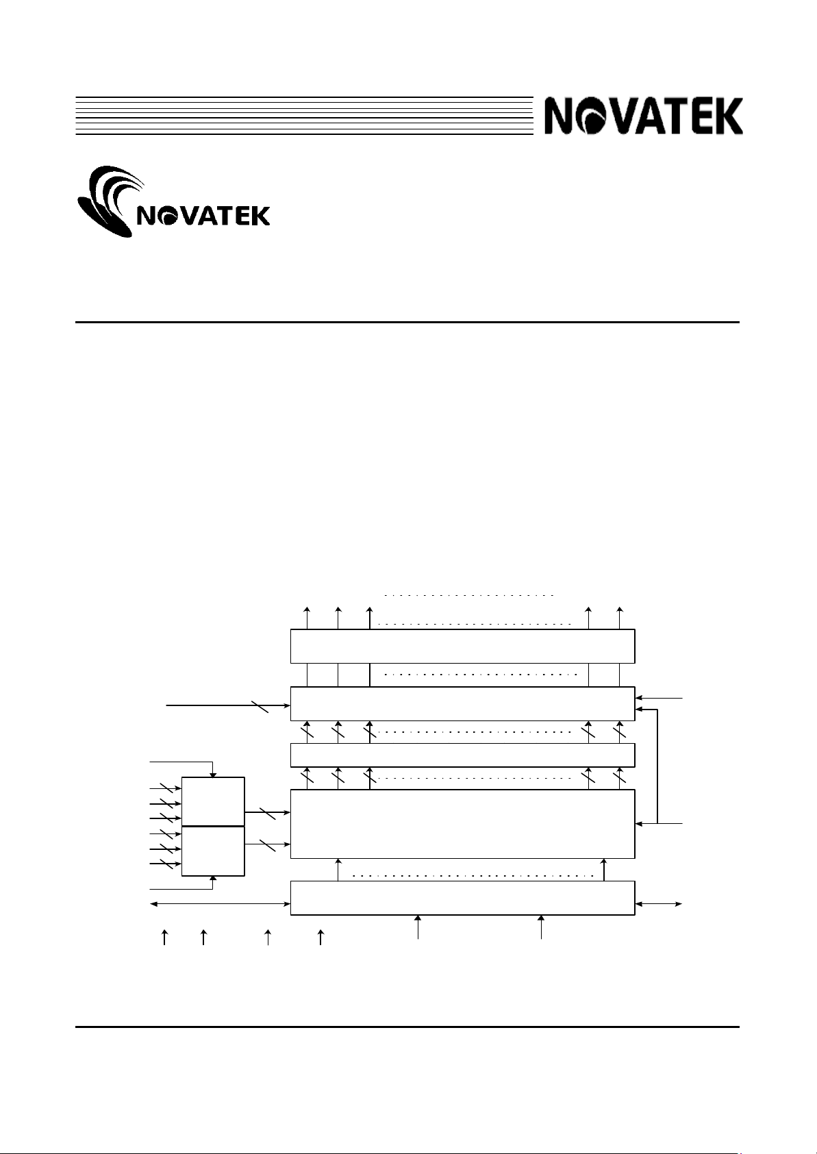
Block diagram
OUT1
OUT2
OUT3
n Power for interface circuit : 2.5~3.6V
n Operating frequency : 65MHz
n Output deviation: 10 ~ 20mV
n Data inversion for reducing EMI
n Cascade function with bi-direction shift control
n CMOS silicon gate ( p-type substrate )
n TCP package
OUT402
OUT401
Out Driver Buffer ( 402 channels )
V1 ~ V10
REV1
D00 ~ D05
D10 ~ D15
D20 ~ D25
D30 ~ D35
D40 ~ D45
D50 ~ D55
REV2
DIO1 DIO2
6
6
Decoder
6
6
6
Decoder
6
Vcc GND AVDD AVSS
10
6
6
18
18
Digit to Analog Converter
6
6
6
Level Shift
6666
Line Latch ( 402 X 6 bits X 2 )
1 67
67-bit Shift Register
CLK
SHL
6
POL
LD
Version 1.0 1 DEC 7 ,2001
Page 2
NT3967
TFT LCD Source Driver
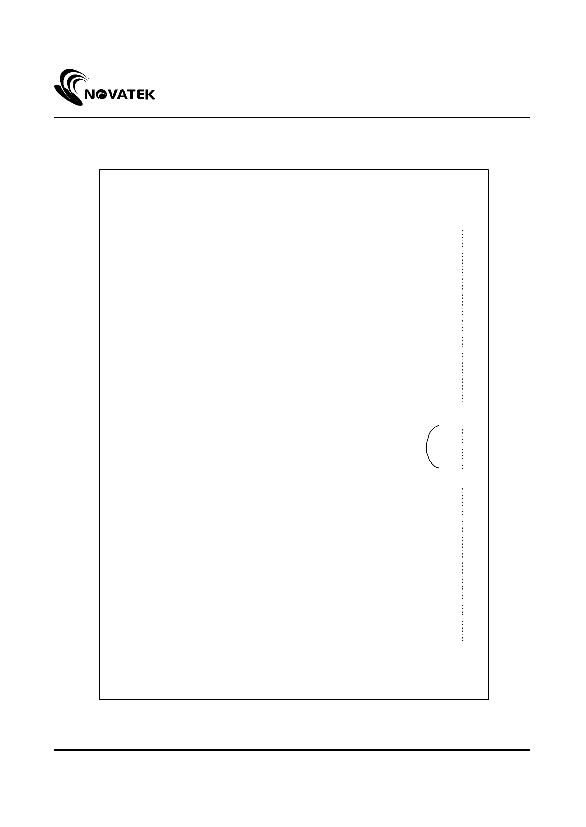
NT3967 Pad configuration (Face up): This figure does not specify the TCP package.
DIO2
D55
D54
D53
D52
D51
D50
D45
D44
D43
D42
D41
D40
D35
D34
D33
D32
D31
D30
Vcc
SHL
V10
V9
V8
V7
V6
AVDD
AVSS
V5
V4
V3
V2
V1
GND
CLK
LD
POL
REV1
REV2
D25
D24
D23
D22
D21
D20
D15
D14
D13
D12
D11
D10
D05
D04
D03
D02
D01
D00
DIO1
OUT402
OUT401
OUT400
OUT399
OUT398
NT3967
OUT206
Dummy
18 pads
Dummy
OUT205
OUT5
OUT4
OUT3
OUT2
OUT1
Version 1.0 2 DEC 7,2001
Page 3
NT3967
“2A”, and so on.
e voltage of these pins must be AVSS< V10< V9<
is latched at the rising edge of the
atched serially onto internal latches at the rising edge of the CLK. After all
with data, 67 clocks, a pulse is shifted out through the DIO2 pin at the rising
ze expansion. In normal
the
start pulse inputs on DIO2, and a pulse outputs through
*Remark: The LD may switch the new data to outputs at anytime even if the line data are not
“POL” value is latched at the rising edge of “LD” to control the polarity of the even or odd outputs.
ive polarity with a voltage range from V1~V5, and
odd outputs are of negative polarity with a voltage range from V6 to V10. On the other hand, if LD
TFT LCD Source Driver
Pin Description
Designation I/O
D05 ~ D00
D15 ~ D10
D25 ~ D20
D35 ~ D30
D45 ~ D40
D55 ~ D50
REV1 I Controls whether the data of D00~D25 are inverted or not.
REV2 I Controls whether the data of D30~D55 are inverted or not, same as REV1.
CLK I Clock input; latching data onto the line latches at the rising edge.
V1 ~ V10 I Gamma correction reference voltage. Th
OUT1 ~
OUT402
SHL I
DIO1
DIO2
LD I Latches the polarity of outputs and switches the new data to outputs.
I Data input. For six 6-bit data,2 pixels, of color data (R, G, B)
DX5 : MSB; DX0 : LSB
When “REV1”=1 these data will be inverted. EX. “00” à “ 3F”, “07”à “ 38”, “15”à
V8<V7<V6; V5<V4 <V3<V2<V1< AVDD
O Output drive signals;
I/O Start pulse signal input/output
Selects left or right shift;
SHL=“1” : DIO1→OUT1,2,3,4,5,6→OUT7,8,9,10,11,12--→OUT397,398,399,400,401,402= DIO2
SHL=“0” : DIO1=OUT1,2,3,4,5,6←OUT7,8,9,10,11,12←-- OUT397,398,399,400,401,402←DIO2
When SHL is applied high (SHL="1"), a start high-pulse on DIO1
CLK. Then the data are l
line latches are filled
edge of the CLK. This function can cascade two or more devices for dot -si
applications, the DIO2 signal of the first device is connected to the DIO1 of the second stage,
DIO2 of the second one is connected to the DIO1 of the third, and so on, like a daisy chain.
In contrast, when SHL is applied low, a
DIO1.
*Remark: The input pulse-width of DIO1/2 may exceed 1 clock-cycle.
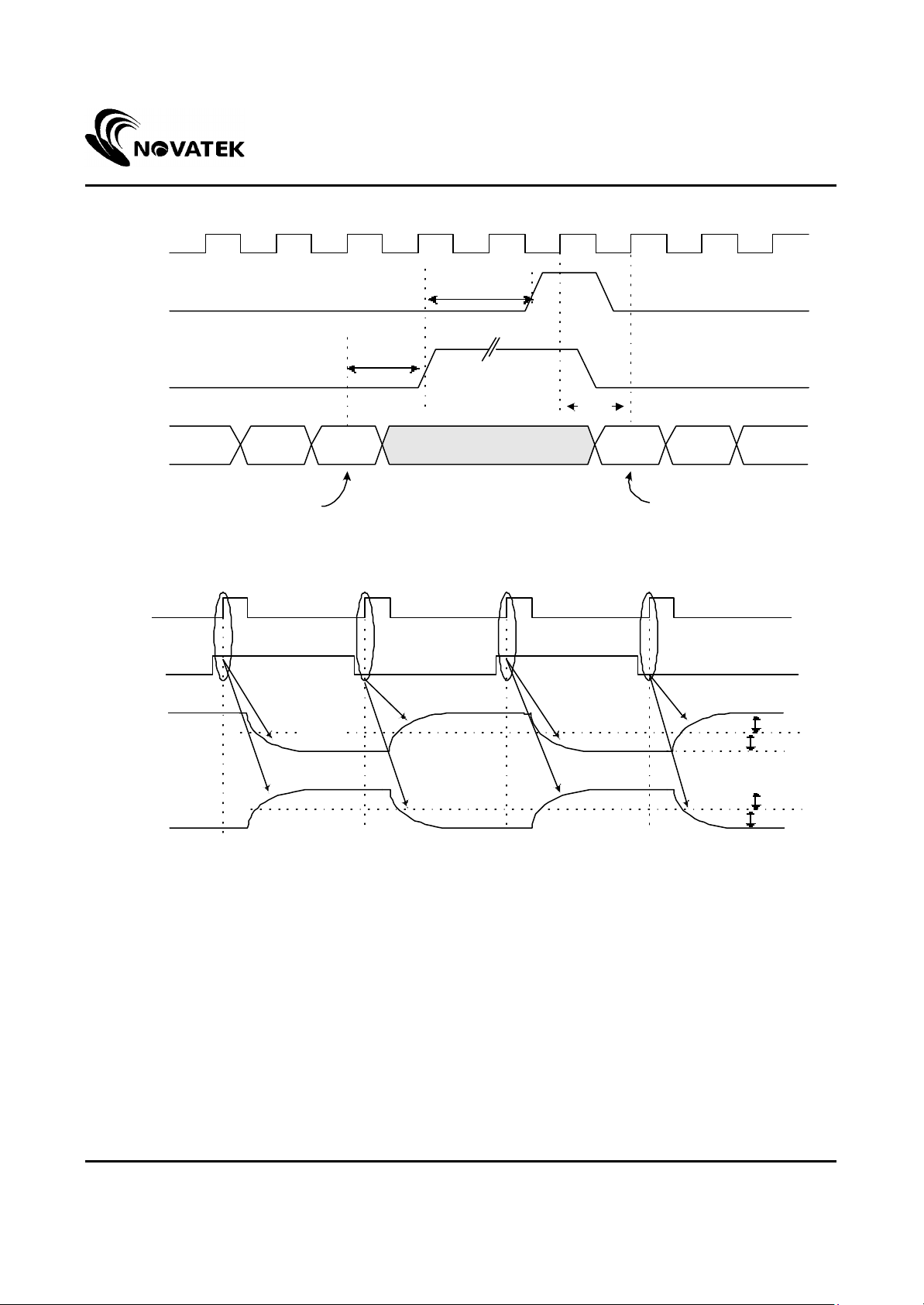
1. At the rising edge, latches the “POL” signal to control the polarity of the outputs.
2. The pin also controls the switch of the line registers that switches the new incoming data
to outputs.
SHL DIO1 DIO2 SHIFT
1 Input Output Right
0 Output Input Left
Description
completely full.
POL I Polarity selector for the dot -inversion control. Available at the rising edge of LD
“POL=1” indicate s that even outputs are of posit
receives low level “POL”, even outputs are of negative polarity and odd outputs are of positive
polarity.
POL=1: Even outputs range from V1 ~ V5
Odd outputs range from V6 ~ V10
POL=0: Even outputs range from V6 ~ V10
Odd outputs range from V1 ~ V5
AVDD I Power supply for analog circuit
AVSS I Ground pin for analog circuit
Vcc I Power supply for digital circuit
GND I Ground pin for digital circuit
Dummy - Dummy pads
Version 1.0 3 DEC 7,2001
Page 4
NT3967
Input Data
TFT LCD Source Driver
Power on/off sequence:
This IC is a high-voltage LCD driver, so it may be damaged by a large current flow when an incorrect power sequence is used.
The recommend ed power on/off sequence is to f irst connect the logical power, Vcc & GND and then the drive power,
AVDD&AVSS with V1~V10 . When shutting off the power, first shut off the drive power and then the logic system, or turn off all
power simultaneously.
Relationship between the order of input data and output channels
(1) SHL=”1”, Start pulse from DIO1, shift right
Output OUT1 OUT2 OUT3 OUT4 OUT5 OUT6 - - - OUT402
Order First data --à Last data
Data D05~D00 D15~D10 D25~D20 D35~D30 D45~D40 D55~D50 - - - D55~D50
(2) SHL=”0”, Start pulse from DIO2, shift left
Output OUT397 OUT398 OUT399 OUT400 OUT401 OUT402 - - - OUT6
Order First data --à Last data
Relationship between input data and output voltage
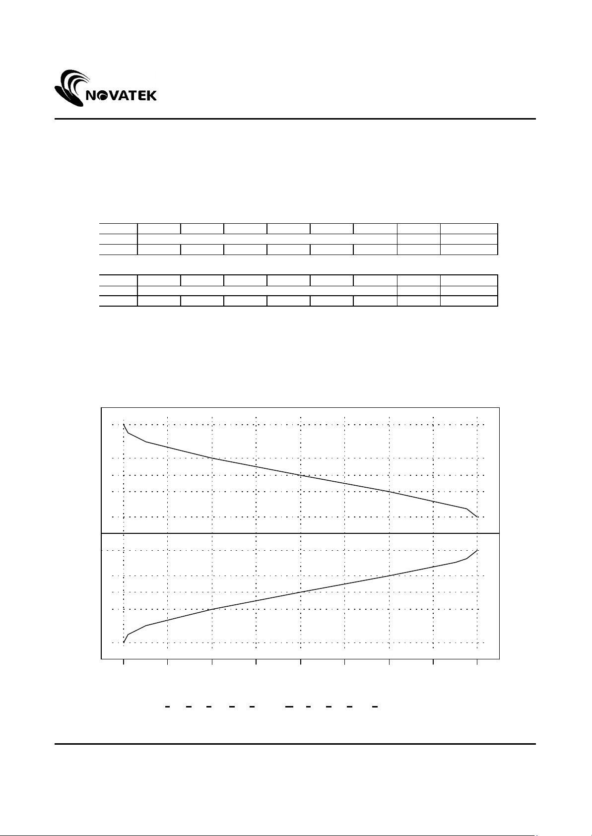
The figure below shows the relationship between the input data and the output voltage with the polarity. The range of
V1~V5 is for positive polarity, and V6 ~ V10 for negative polarity. Please refer to the following page to get the relative resistor
value and voltage calculation method.
Gamma correction diagram
AVDD
Data D05~D00 D15~D10 D25~D20 D35~D30 D45~D40 D55~D50 - - - D55~D50
Vout
V1
V2
V3
V4
V5
Vcom
V6
V7
V8
V9
V10
AVSS
08H
10H00H 18H 20H 28H 30H 38H 3FH
Positive polarity
Negative polarity
Remark: AV DD-0.1 > V1 > V2 > V3 > V4 > V5; V6 > V7 > V8 > V9 > V10 >AVSS+0.1V
Version 1.0 4 DEC 7,2001
Page 5
NT3967
TFT LCD Source Driver
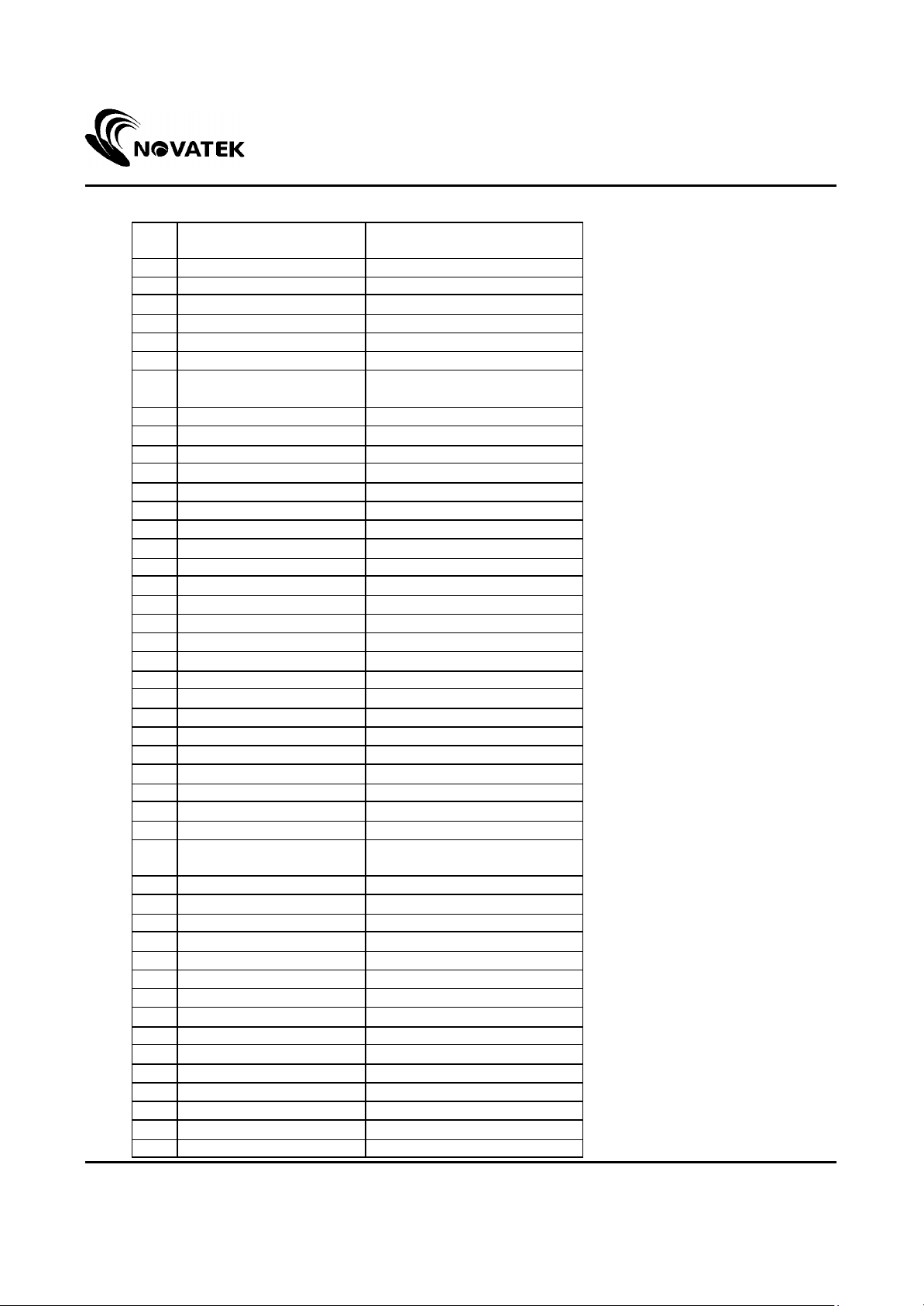
Gamma correction resistor
V1, V10
8.05K
V2, V9
2.75K
V3, V8
Name Resistor
R0 800 R32 100
R1 750 R33
R2 700 R34
R3 650 R35
R4 600 R36
R5 550 R37
R6 550 R38
R7 500 R39
R8 500 R40
R9 400 R41
R10 400 R42
R11 R43
R12 R44
R13 R45
R14 R46
R15 R47
R16 300 R48
R17 R49
R18 R50
R19 R51
R20 R52
R21 R53
R24 R56
R25 R57
R26 R58
R27 R59 250
R28 R60 300
R29 R61 500
R30 R62 800
R31
350
350
350
300
300
250
250
250
200
200
200
150
150
150
150
100
100
100
100
100
Name Resistor
100
100
100
100
100
100
100
100
100
100
100
100
100
100
100
100
100
100
100
100
150
150R22 R54
150R23 R55
200
200
250
V3, V8
1.6K
V4, V7
3.45K
V5, V6
Total impedance, Rn=R0 ~ R62, equals 15.85K
Version 1.0 5 DEC 7,2001
Page 6
NT3967
V3) X2450/2750
V4) X 1500/1600
TFT LCD Source Driver
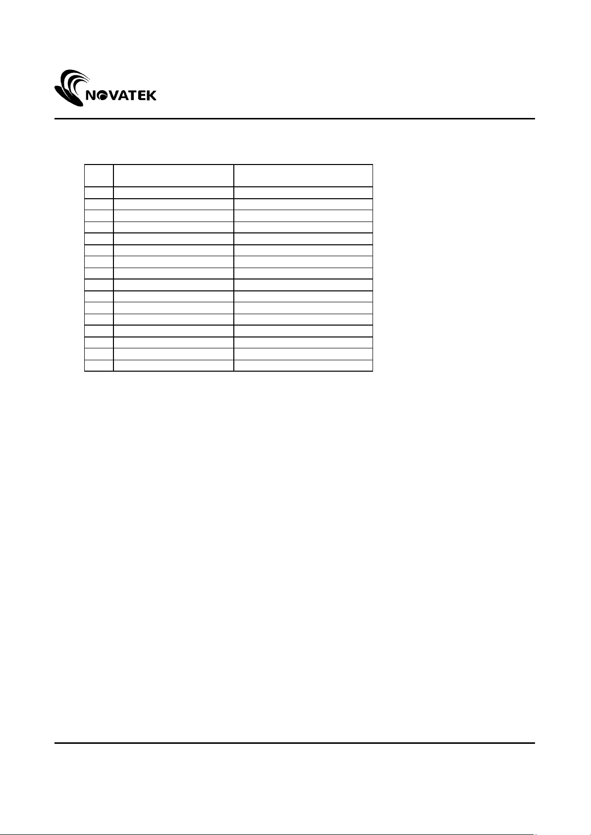
Output Voltage VS Input Data
Data Output Voltage
( Positive polarity )
00H V1 V10
01H
02H
03H
04H
05H
06H
07H
08H
09H
0AH
0BH
0CH
0DH
0EH
0FH
10H
11H
12H
13H
14H
15H
16H
17H
18H
19H
1AH
1BH
1CH
1DH
1EH
1FH
20H
21H
22H
23H
24H
25H
26H
27H
28 H
29H
2AH
2BH
2CH
2DH
2EH
2FH
Version 1.0 6 DEC 7,2001
V2 + ( V1 – V2) X 7250/8050
V2 + ( V1 – V2) X 6500/8050 V10 + ( V9 – V10) X 1550/8050
V2 + ( V1 – V2) X 5800/8050 V10 + ( V9 – V10) X 2250/8050
V2 + ( V1 – V2) X 5150/8050 V10 + ( V9 – V10) X 2900/8050
V2 + ( V1 – V2) X 4550/8050 V10 + ( V9 – V10) X 3500/8050
V2 + ( V1 – V2) X 4000/8050 V10 + ( V9 – V10) X 4050/8050
V2 + ( V1 – V2) X 3450/8050 V10 + ( V9 – V10) X 4600/8050
V2 + ( V1 – V2) X 2950/8050 V10 + ( V9 – V10) X 5100/8050
V2 + ( V1 – V2) X 2450/8050 V10 + ( V9 – V10) X 5600/8050
V2 + ( V1 – V2) X 2050/8050 V10 + ( V9 – V10) X 6000/8050
V2 + ( V1 – V2) X 1650/8050 V10 + ( V9 – V10) X 6400/8050
V2 + ( V1 – V2) X 1300/8050 V10 + ( V9 – V10) X 6750/8050
V2 + ( V1 – V2) X 950/8050
V2 + ( V1 – V2) X 600/8050
V2 + ( V1 – V2) X 300/8050
V3 + (V2 –
V3 + (V2 – V3) X 2200/2750
V3 + (V2 – V3) X 1950/2750
V3 + (V2 – V3) X 1700/2750
V3 + (V2 – V3) X 1500/2750
V3 + (V2 – V3) X 1300/2750
V3 + (V2 – V3) X 1100/2750
V3 + (V2 – V3) X 950/2750
V3 + (V2 – V3) X 800/2750
V3 + (V2 – V3) X 650/2750
V3 + (V2 – V3) X 500/2750
V3 + (V2 – V3) X 400/2750
V3 + (V2 – V3) X 300/2750
V3 + (V2 – V3) X 200/2750
V3 + (V2 – V3) X 100/2750
V4 + (V3 –
V4 + (V3 – V4) X 1400/1600
V4 + (V3 – V4) X 1300/1600
V4 + (V3 – V4) X 1200/1600
V4 + (V3 – V4) X 1100/1600
V4 + (V3 – V4) X 1000/1600
V4 + (V3 – V4) X 900/1600
V4 + (V3 – V4) X 800/1600
V4 + (V3 – V4) X 700/1600
V4 + (V3 – V4) X 600/1600
V4 + (V3 – V4) X 500/1600
V4 + (V3 – V4) X 400/1600
V4 + (V3 – V4) X 300/1600
V4 + (V3 – V4) X 200/1600
V4 + (V3 – V4) X 100/1600
V2 V9
V3 V8
Output Voltage
( Negative polarity )
V10 + ( V9 – V10) X 800/8050
V10 + ( V9 – V10) X 7100/8050
V10 + ( V9 – V10) X 7450/8050
V10 + ( V9 – V10) X 7750/8050
V9 + ( V8 – V9) X 300/2750
V9 + ( V8 – V9) X 550/2750
V9 + ( V8 – V9) X 800/2750
V9 + ( V8 – V9) X 1050/2750
V9 + ( V8 – V9) X 1250/2750
V9 + ( V8 – V9) X 1450/2750
V9 + ( V8 – V9) X 1650/2750
V9 + ( V8 – V9) X 1800/2750
V9 + ( V8 – V9) X 1950/2750
V9 + ( V8 – V9) X 2100/2750
V9 + ( V8 – V9) X 2250/2750
V9 + ( V8 – V9) X 2350/2750
V9 + ( V8 – V9) X 2450/2750
V9 + ( V8 – V9) X 2550/2750
V9 + ( V8 – V9) X 2650/2750
V8 + ( V7 – V8) X 100/1600
V8 + ( V7 – V8) X 200/1600
V8 + ( V7 – V8) X 300/1600
V8 + ( V7 – V8) X 400/1600
V8 + ( V7 – V8) X 500/1600
V8 + ( V7 – V8) X 600/1600
V8 + ( V7 – V8) X 700/1600
V8 + ( V7 – V8) X 800/1600
V8 + ( V7 – V8) X 900/1600
V8 + ( V7 – V8) X 1000/1600
V8 + ( V7 – V8) X 1100/1600
V8 + ( V7 – V8) X 1200/1600
V8 + ( V7 – V8) X 1300/1600
V8 + ( V7 – V8) X 1400/1600
V8 + ( V7 – V8) X 1500/1600
Page 7
NT3967
TFT LCD Source Driver
Output Voltage VS Input Data (continued)
Data Output Voltage
( Positive polarity )
30H
31H
32H
33H
34H
35H
36H
37H
38H
39H
3AH
3BH
3CH
3DH
3EH
3FH
V5 + (V4 – V5) X 3350/3450
V5 + (V4 – V5) X 3250/3450
V5 + (V4 – V5) X 3150/3450
V5 + (V4 – V5) X 3050/3450
V5 + (V4 – V5) X 2950/3450
V5 + (V4 – V5) X 2800/3450
V5 + (V4 – V5) X 2650/3450
V5 + (V4 – V5) X 2500/3450
V5 + (V4 – V5) X 2300/3450
V5 + (V4 – V5) X 2100/3450
V5 + (V4 – V5) X 1850/3450
V5 + (V4 – V5) X 1600/3450
V5 + (V4 – V5) X 1300/3450
V5 + (V4 – V5) X 800/3450
V4 V7
V5 V6
Output Voltage
( Negative polarity )
V7 + ( V6 – V7) X 100/3450
V7 + ( V6 – V7) X 200/3450
V7 + ( V6 – V7) X 300/3450
V7 + ( V6 – V7) X 400/3450
V7 + ( V6 – V7) X 500/3450
V7 + ( V6 – V7) X 650/3450
V7 + ( V6 – V7) X 800/3450
V7 + ( V6 – V7) X 950/3450
V7 + ( V6 – V7) X 1150/3450
V7 + ( V6 – V7) X 1350/3450
V7 + ( V6 – V7) X 1600/3450
V7 + ( V6 – V7) X 1850/3450
V7 + ( V6 – V7) X 2150/3450
V7 + ( V6 – V7) X 2650/3450
Version 1.0 7 DEC 7,2001
Page 8
NT3967
TFT LCD Source Driver
Absolute Maximum Ratings* *Comments
Digital supply voltage, Vcc -0.5V to 5V
Analog supply voltage, AVDD -0.5V to +11V
Supply voltage, V1~ V10 -0.3 ~AVDD+0.3
Digital input voltage -0.5V to Vcc+0.5V
Output voltage, DIO1 & DIO2 -0.5V to Vcc+0.5V
Output voltage,OUT1~OUT420 -0.5V to AV DD+0.5V
Storage temperature
Operating temperature -10℃ to 75℃
-55℃ to 100℃
DC Electrical Characteristics (Vcc =2.5~3.6V , AV DD=6.5~10V, AVSS=GND=0V, TA=-10℃~75℃)
(For the digital circuit)
Supply Voltage Vcc 2.5 - 3.6 V Digital power
Low Level Input Voltage Vil 0 - 0.3xVcc V For the digital circuit
High Level Input Voltage Vih 0.7xVcc - Vcc V For the digital circuit
High Level Output Voltage Voh Vcc-0.3V - - V DIO1/2, Ioh=500uA
Low Level Output Voltage Vol - - GND+0.3V V DIO1/2, Iol=-500uA
Input Leakage Current Ii - - +1
Digital Stand-by current Ist - - 50
Digital Operating Current Icc - 3 5 mA Fclk=40 MHz, FLD=50KHz
Parameter Symbol Min. Typ. Max. Unit Conditions
(For the analog circuit)
Parameter
Supply Voltage AVDD 6.5 8.4 10 V For the analog circuit power
Input level of V1 ~ V5 Vref 0.4AVDD - AVDD-0.1 V Gamma correction voltage
Input level of V6 ~ V10 Vref 0.1 0.6AVDD V Gamma correction voltage
Voltage Output Deviation Vvd
Voltage Output Offset Voc +10 mV
Dynamic Range of Output Vdr 0.1 - AVDD-0.1 V OUT1 ~ OUT402
Sinking Current of outputs IOL -150 -180 -
Driving Current of outputs IOH 150 200 Impedance of Gamma
Correction
Analog Operating Current IDD - 3 6 mA No load, Fclk=33MHz, FLD=50KHz
Symbol Min.
Ri 0.8*Rn Rn 1.3*Rn ohm Rn=15850 ohm, from V1 ~ V5 & V6~V10
Typ.
- +20 +25 mV Vo=0.1V ~ 1.5V & AVDD-1.5 ~ AVDD +10 +20 mV Vo=1.5V ~ AVDD-1.5V
Stresses above those listed under "Absolute Maximum
Ratings" may cause permanent damage to the device.
These are stress ratings only. Functional operation of this
device at these or under any other conditions above those
indicated in the operational sections of this specification are
not implied and exposure to absolute maximum rating
conditions for extended periods may affect device reliability.
For the digital circuit
µA
CLK is stoppe d, DIO1/2 No load
µA
Max.
Unit
µA
µA
0.1V
OUT1 ~ OUT402; Vo=0.1V V.S 1.1V
OUT1 ~ OUT402; Vo=9.9V V.S 8.9V
Conditions
Version 1.0 8 DEC 7,2001
Page 9

NT3967
TFT LCD Source Driver
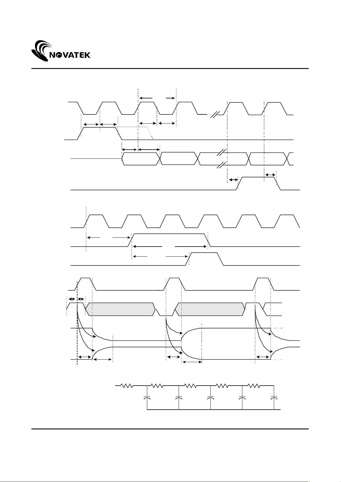
AC Electrical Characteristics 1 (Vcc =3.0~3.6V , AVDD=6.5~10V, AVSS=GND=0V, TA= - 10~75℃)
Parameter Symbol Min. Typ. Max. Unit Conditions
CLK frequency Fclk - - 65 Mhz
CLK period cycle Tcph 15 - - ns
CLK pulse width Tcw 6 - - ns
Data set -up time Tsu 4 - - ns D00 ~ D55, REVx and DIO1/2 to CLK
Data hold time Thd 2 - - ns D00 ~ D55, REVx and DIO1/2 to CLK
Propagation delay of DIO2/1 Tphl 6 - 11 ns CL=25pF ( Output )
Time that the last data to LD Tld 1 - - Tcph
Pulse width of LD Twld 2 - - Tcph
Time that LD to DIO1/2 Tlds 2 - - Tcph
POL set-up time Tpsu 6 - - ns POL to LD
POL hold time Tphd 6 - - ns POL to LD
Output stable time Tst - 4.5 9 us 96% final value or below with 30mV
Output loading
CL
-
-
75
AC Electrical Characteristics 2 (Vcc =2.5~3.0V , AV DD=6.5~10V, AVSS=GND=0V, TA= -10~75℃)
precision , CL=75pF, R=5K ohm
pF For OUT1 ~ OUT402
CLK frequency Fclk - - 45 Mhz
CLK period cycle Tcph 22 - - ns
CLK pulse width Tcw 8 - - ns
Data set -up time Tsu 6 - - ns D00 ~ D55, REVx and DIO1/2 to CLK
Data hold time Thd 2 - - ns D00 ~ D55, REVx and DIO1/2 to CLK
Propagation delay of DIO2/1 Tphl - - 15 ns CL=25pF ( Output )
Time that the last data to LD Tld 1 - - Tcph
Pulse width of LD Twld 2 - - Tcph
Time that LD to DIO1/2 Tlds 2 - - Tcph
POL set -up time Tpsu 6 - - ns POL to LD
POL hold time Tphd 6 - - ns POL to LD
Output stable time Tst - 4.5 9 us 96% final value or below with 30mV
Output loading CL - -
Parameter Symbol Min. Typ. Max. Unit Conditions
precision , CL=75pF, R=5K ohm
75
pF For OUT1 ~ OUT402
Version 1.0 9 DEC 7,2001
Page 10
NT3967
TFT LCD Source Driver
Timing Diagram
Tcph
CLK
DIO1/2
( Input )
Data,
REVx
DIO1/2
( Output )
CLK
LD
DIO1/2
( Input )
Tsu Thd
Last
Tld
Tsu
Thd
TcwTcw
Second data
Twld
Tlds
66 67
Last dataFirst data
Tphl
Tphl
LD
Tpdh
Tpsu
POL
96%
Odd outputs
High-Z High-Z
Even outputs Negative
Output load condition :
Tst
1K
High-Z
1K
Tst
1K
96%
1K
1K
Positive
Output
15P
15P
15P
15P
15P
Vcom
Version 1.0 10 DEC 7,2001
Page 11
NT3967
TFT LCD Source Driver
Function opera tion
CLK
DIO1/2
( Input )
LD
Data,
REVx
LD
POL
Odd Outputs
2CLK ( min.)
1CLK ( min.)
1CLK
N-2 3
N-1 N 1 2
Last Data First Data
Vcom
V1 ~V5
V6 ~V10
Even Outputs
Version 1.0 11 DEC 7,2001
V1 ~V5
V6 ~V10
 Loading...