

Page 1
TL/C/5171
NSC800 High-Performance Low-Power CMOS Microprocessor
June 1992
NSC800TMHigh-Performance
Low-Power CMOS Microprocessor
General Description
The NSC800 is an 8-bit CMOS microprocessor that functions as the central processing unit (CPU) in National Semiconductor’s NSC800 microcomputer family. National’s
microCMOS technology used to fabricate this device provides system designers with performance equivalent to
comparable NMOS products, but with the low power advantage of CMOS. Some of the many system functions incorporated on the device, are vectored priority interrupts, refresh
control, power-save feature and interrupt acknowledge. The
NSC800 is available in dual-in-line and surface mounted
chip carrier packages.
The system designer can choose not only from the dedicated CMOS peripherals that allow direct interfacing to the
NSC800 but from the full line of National’s CMOS products
to allow a low-power system solution. The dedicated peripherals include NSC810A RAM I/O Timer, NSC858 UART,
and NSC831 I/O.
All devices are available in commercial, industrial and military temperature ranges along with two added reliability
flows. The first is an extended burn in test and the second is
the military class C screening in accordance with Method
5004 of MIL-STD-883.
Features
Y
Fully compatible with Z80Éinstruction set:
Powerful set of 158 instructions
10 addressing modes
22 internal registers
Y
Low power: 50 mW at 5V V
CC
Y
Unique power-save feature
Y
Multiplexed bus structure
Y
Schmitt trigger input on reset
Y
On-chip bus controller and clock generator
Y
Variable power supply 2.4Vb6.0V
Y
On-chip 8-bit dynamic RAM refresh circuitry
Y
Speed: 1.0 ms instruction cycle at 4.0 MHz
NSC800-4 4.0 MHz
NSC800-35 3.5 MHz
NSC800-3 2.5 MHz
NSC800-1 1.0 MHz
Y
Capable of addressing 64k bytes of memory and 256
I/O devices
Y
Five interrupt request lines on-chip
Block Diagram
TL/C/5171– 73
NSC800TMis a trademark of National Semiconductor Corp.
TRI-STATE
É
is a registered trademark of National Semiconductor Corp.
Z80
É
is a registered trademark of Zilog Corp.
C
1995 National Semiconductor Corporation RRD-B30M105/Printed in U. S. A.
Page 2

Table of Contents
1.0 ABSOLUTE MAXIMUM RATINGS
2.0 OPERATING CONDITIONS
3.0 DC ELECTRICAL CHARACTERISTICS
4.0 AC ELECTRICAL CHARACTERISTICS
5.0 TIMING WAVEFORMS
NSC800 HARDWARE
6.0 PIN DESCRIPTIONS
6.1 Input Signals
6.2 Output Signals
6.3 Input/Output Signals
7.0 CONNECTION DIAGRAMS
8.0 FUNCTIONAL DESCRIPTION
8.1 Register Array
8.2 Dedicated Registers
8.2.1 Program Counter
8.2.2 Stack Pointer
8.2.3 Index Register
8.2.4 Interrupt Register
8.2.5 Refresh Register
8.3 CPU Working and Alternate Register Sets
8.3.1 CPU Working Registers
8.3.2 Alternate Registers
8.4 Register Functions
8.4.1 Accumulator
8.4.2 F RegisterÐFlags
8.4.3 Carry (C)
8.4.4 Adds/Subtract (N)
8.4.5 Parity/Overflow (P/V)
8.4.6 Half Carry (H)
8.4.7 Zero Flag (Z)
8.4.8 Sign Flag (S)
8.4.9 Additional General Purpose Registers
8.4.10 Alternate Configurations
8.5 Arithmetic Logic Unit (ALU)
8.6 Instruction Register and Decoder
9.0 TIMING AND CONTROL
9.1 Internal Clock Generator
9.2 CPU Timing
9.3 Initialization
9.4 Power Save Feature
9.0 TIMING AND CONTROL
9.5 Bus Access Control
9.6 Interrupt Control
NSC800 SOFTWARE
10.0 INTRODUCTION
11.0 ADDRESSING MODES
11.1 Register
11.2 Implied
11.3 Immediate
11.4 Immediate Extended
11.5 Direct Addressing
11.6 Register Indirect
11.7 Indexed
11.8 Relative
11.9 Modified Page Zero
11.10 Bit
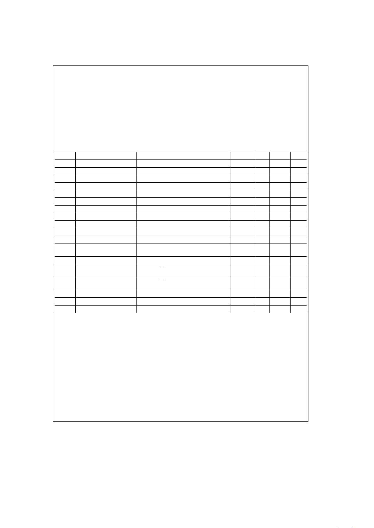
12.0 INSTRUCTION SET
12.1 Instruction Set Index/Alphabetical
12.2 Instruction Set Mnemonic Notation
12.3 Assembled Object Code Notation
12.4 8-Bit Loads
12.5 16-Bit Loads
12.6 8-Bit Arithmetic
12.7 16-Bit Arithmetic
12.8 Bit Set, Reset, and Test
12.9 Rotate and Shift
12.10 Exchanges
12.11 Memory Block Moves and Searches
12.12 Input/Output
12.13 CPU Control
12.14 Program Control
12.15 Instruction Set: Alphabetical Order
12.16 Instruction Set: Numerical Order
13.0 DATA ACQUISITION SYSTEM
14.0 NSC800M/883B MIL STD 883/CLASS C
SCREENING
15.0 BURN-IN CIRCUITS
16.0 ORDERING INFORMATION
17.0 RELIABILITY INFORMATION
2
Page 3
1.0 Absolute Maximum Ratings (Note 1)
If Military/Aerospace specified devices are required,
please contact the National Semiconductor Sales
Office/Distributors for availability and specifications.
Storage Temperature
b
65§Ctoa150§C
Voltage on Any Pin
with Respect to Ground
b
0.3V to V
CC
a
0.3V
Maximum V
CC
7V
Power Dissipation 1W
Lead Temp. (Soldering, 10 seconds) 300
§
C
2.0 Operating Conditions
NSC800-1
x
T
A
e
0§Ctoa70§C
T
A
eb
40§Ctoa85§C
NSC800-3
x
T
A
e
0§Ctoa70§C
T
A
eb
40§Ctoa85§C
T
A
eb
55§Ctoa125§C
NSC800-35/883C
x
T
A
eb
55§Ctoa125§C
NSC800-4
x
T
A
e
0§Ctoa70§C
T
A
eb
40§Ctoa85§C
NSC800-4MIL
x
T
A
eb
55§Ctoa90§C
3.0 DC Electrical Characteristics V
CC
e
5Vg10%, GNDe0V, unless otherwise specified.
Symbol Parameter Conditions Min Typ Max Units
V
IH
Logical 1 Input Voltage 0.8 V
CC
V
CC
V
V
IL
Logical 0 Input Voltage 0 0.2 V
CC
V
V
HY
Hysteresis at RESET IN input V
CC
e
5V 0.25 0.5 V
V
OH1
Logical 1 Output Voltage I
OUT
eb
1.0 mA 2.4 V
V
OH2
Logical 1 Output Voltage I
OUT
eb
10 mAV
CC
b
0.5 V
V
OL1
Logical 0 Output Voltage I
OUT
e
2 mA 0 0.4 V
V
OL2
Logical 0 Output Voltage I
OUT
e
10 mA 0 0.1 V
I
IL
Input Leakage Current 0sV
IN
s
V
CC
b
10.0 10.0 mA
I
OL
Output Leakage Current 0sV
IN
s
V
CC
b
10.0 10.0 mA
I
CC
Active Supply Current I
OUT
e
0, f
(XIN)
e
2 MHz, T
A
e
25§C 8 11 mA
I
CC
Active Supply Current I
OUT
e
0, f
(XIN)
e
5 MHz, T
A
e
25§C1015mA
I
CC
Active Supply Current I
OUT
e
0, f
(XIN)
e
7 MHz,
15 21 mA
T
A
e
25§C
I
CC
Active Supply Current I
OUT
e
0, f
(XIN)
e
8 MHz, T
A
e
25§C1521mA
I
Q
Quiescent Current I
OUT
e
0, PSe0, V
IN
e
0orV
IN
e
V
CC
25mA
f
(XIN)
e
0 MHz, T
A
e
25§C, X
IN
e
0, CLKe1
I
PS
Power-Save Current I
OUT
e
0, PSe0, V
IN
e
0orV
IN
e
V
CC
57mA
f
(XIN)
e
5.0 MHz , T
A
e
25
§
C
IN
Input Capacitance 610pF
C
OUT
Output Capacitance 812pF
VCCPower Supply Voltage (Note 2) 2.4 5 6 V
Note 1: Absolute Maximum Ratings indicate limits beyond which permanent damage may occur. Continuous operation at these limits is not intended and should be
limited to those conditions specified under DC Electrical Characteristics.
Note 2: CPU operation at lower voltages will reduce the maximum operating speed. Operation at voltages other than 5V
g
10% is guaranteed by design, not
tested.
3
Page 4
4.0 AC Electrical Characteristics V
CC
e
5Vg10%, GNDe0V, unless otherwise specified
Symbol Parameter
NSC800-1 NSC800-3 NSC800-35 NSC800-4
Units Notes
Min Max Min Max Min Max Min Max
t
X
Period at XIN and XOUT 500 3333 200 3333 142 3333 125 3333 ns
Pins
T Period at Clock Output 1000 6667 400 6667 284 6667 250 6667 ns
(
e
2tX)
t
R
Clock Rise Time 110 110 90 80 ns Measured from
10%–90% of signal
t
F
Clock Fall Time 70 60 55 50 ns Measured from
10%–90% of signal
t
L
Clock Low Time 435 150 90 80 ns 50% duty cycle, square
wave input on XIN
t
H
Clock High Time 450 145 85 75 ns 50% duty cycle, square
wave input on XIN
t
ACC(OP)
ALE to Valid Data 1340 490 340 300 ns Add t for each WAIT STATE
t
ACC(MR)
ALE to Valid Data 1875 620 405 360 ns Add t for each WAIT STATE
t
AFR
AD(0–7) Float after 0 0 0 0 ns
RD
Falling
t
BABE
BACK Rising to Bus 1000 400 300 250 ns
Enable
t
BABF
BACK Falling to 50 50 50 50 ns
Bus Float
t
BACL
BACK Fall to CLK 425 125 60 55 ns
Falling
t
BRH
BREQ Hold Time 0 0 0 0 ns
t
BRS
BREQ Set-Up Time 100 50 50 45 ns
t
CAF
Clock Falling ALE 0 70 0 65 0 60 0 55 ns
Falling
t
CAR
Clock Rising to ALE 0 100 0 100 0 90 0 80 ns
Rising
t
CRD
Clock Rising to 100 90 90 80 ns
Read Rising
t
CRF
Clock Rising to 80 70 70 65 ns
Refresh Falling
t
DAI
ALE Falling to INTA 445 160 95 85 ns
Falling
t
DAR
ALE Falling to 400 575 160 250 100 180 90 160 ns
RD
Falling
t
DAW
ALE Falling to 900 1010 350 420 225 300 200 265 ns
WR
Falling
t
D(BACK)1
ALE Falling to BACK 2460 975 635 560 ns Add t for each WAIT state
Falling Add t for opcode fetch cycles
t
D(BACK)2
BREQ Rising to BACK 500 1610 200 700 140 540 125 475 ns
Rising
t
D(I)
ALE Falling to INTR, 1360 475 284 250 ns Add t for each WAIT state
NMI
, RSTA-C,PS, Add t for opcode fetch cycles
BREQ
, Inputs Valid
t
DPA
Rising PS to 500 1685 200 760 140 580 125 510 ns See
Figure 14
also
Falling ALE
t
D(WAIT)
ALE Falling to 550 250 170 125 ns
WAIT
Input Valid
OPÐ Opcode Fetch
MRÐ Memory Read
4
Page 5
4.0 AC Electrical Characteristics V
CC
e
5Vg10%, GNDe0V, unless otherwise specified (Continued)
Symbol Parameter
NSC800-1 NSC800-3 NSC800-35 NSC800-4
Units Notes
Min Max Min Max Min Max Min Max
T
H(ADH)1
A(8–15) Hold Time During 0 0 0 0 ns
Opcode Fetch
T
H(ADH)2
A(8–15) Hold Time During 400 100 85 60 ns
Memory or IO, RD
and WR
T
H(ADL)
AD(0–7) Hold Time 100 60 35 30 ns
T
H(WD)
Write Data Hold Time 400 100 85 75 ns
t
INH
Interrupt Hold Time 0 0 0 0 ns
t
INS
Interrupt Set-Up Time 100 50 50 45 ns
t
NMI
Width of NMI Input 50 30 25 20 ns
t
RDH
Data Hold after Read 0 0 0 0 ns
t
RFLF
RFSH Rising to ALE 60 50 45 40 ns
Falling
t
RL(MR)
RD Rising to ALE Rising 390 100 50 45 ns
(Memory Read)
t
S(AD)
AD(0–7) Set-Up Time 300 45 45 40 ns
t
S(ALE)
A(8–15), SO, SI, IO/M 350 70 55 50 ns
Set-Up Time
t
S(WD)
Write Data Set-Up Time 385 75 35 30 ns
t
W(ALE)
ALE Width 430 130 115 100 ns
t
WH
WAIT Hold Time 0 0 0 0 ns
t
W(I)
Width of INTR, RSTA-C, 500 200 140 125 ns
PS
, BREQ
t
W(INTA)
INTA Strobe Width 1000 400 225 200 ns Add two t states for first
INTA of each interrupt
response string Add t for
each WAIT state
t
WL
WR Rising to ALE Rising 450 130 70 70 ns
t
W(RD)
Read Strobe Width During 960 360 210 185 ns Add t for each WAIT
State Add t/2 for Memory
Opcode Fetch
Read Cycles
t
W(RFSH)
Refresh Strobe Width 1925 725 450 395 ns
t
WS
WAIT Set-Up Time 100 70 60 55 ns
t
W(WAIT)
WAIT Input Width 550 250 195 175 ns
t
W(WR)
Write Strobe Width 985 370 250 220 ns Add t for each WAIT state
t
XCF
XIN to Clock Falling 25 100 15 95 5 90 5 80 ns
t
XCR
XIN to Clock Rising 25 85 15 85 5 90 5 80 ns
Note 1: Test conditions: te1000 ns for NSC800-1, 400 ns for NSC800, 285 ns for NSC800-35, 250 ns for NSC800-4.
Note 2: Output timings are measured with a purely capacitive load of 100 pF.
5
Page 6
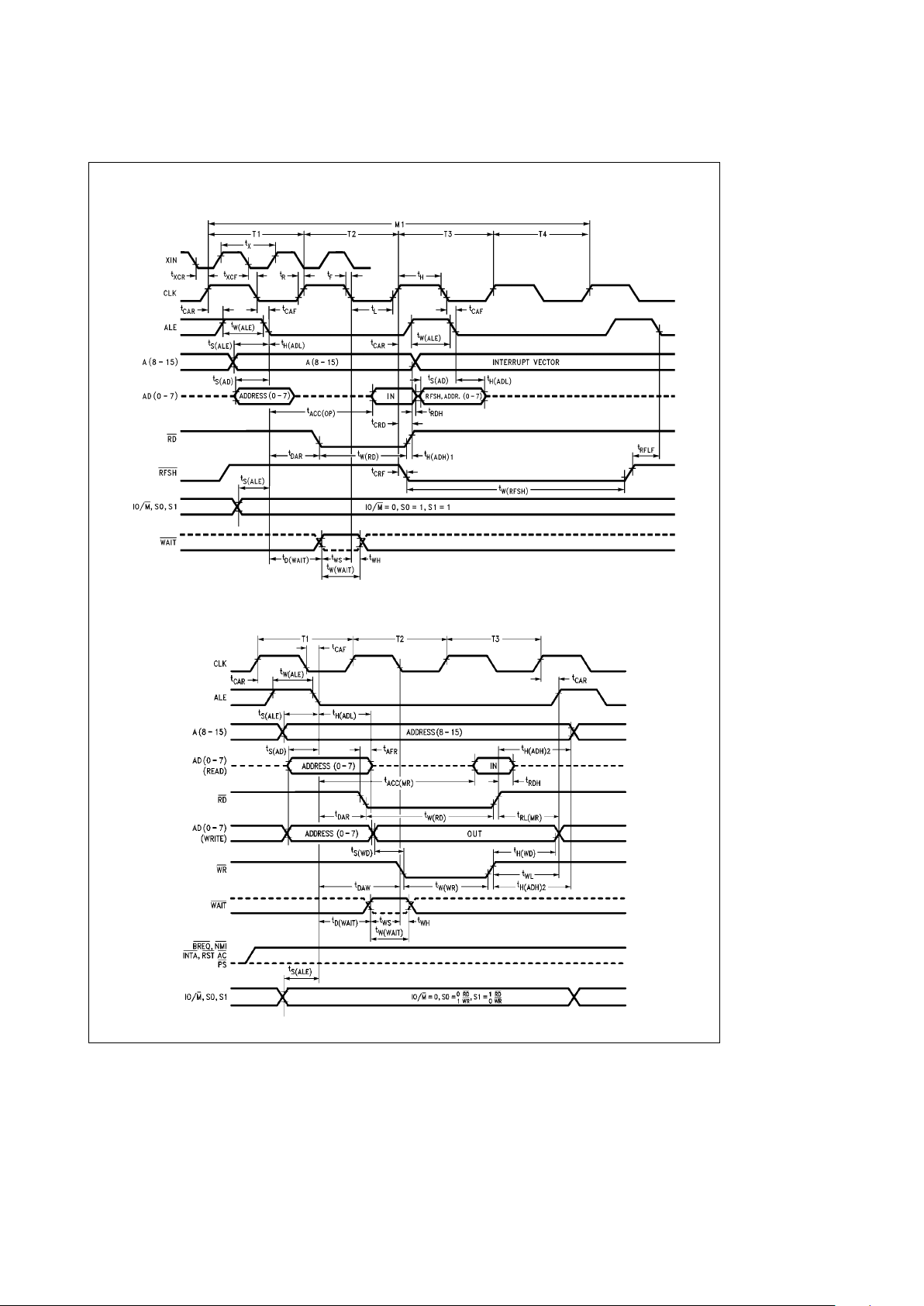
5.0 Timing Waveforms
Opcode Fetch Cycle
TL/C/5171– 3
Memory Read and Write Cycle
TL/C/5171– 4
6
Page 7
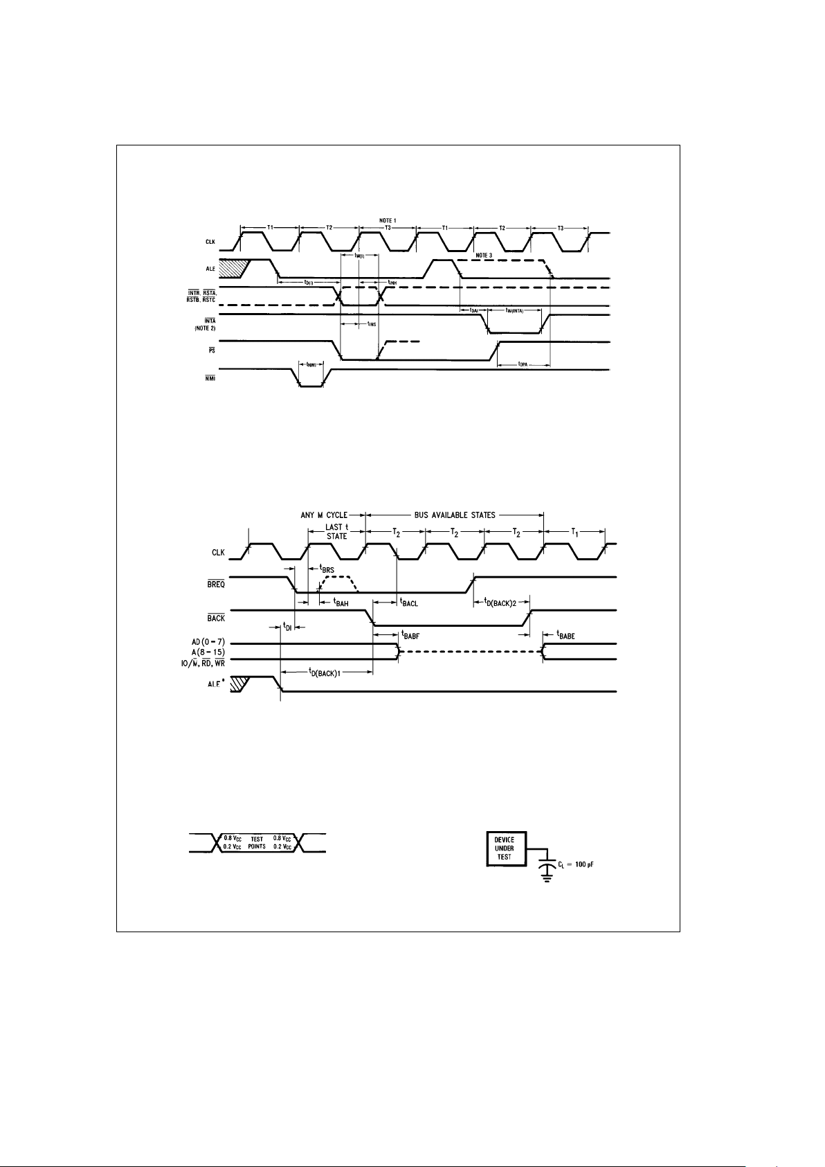
5.0 Timing Waveforms (Continued)
InterruptÐPower-Save Cycle
TL/C/5171– 5
Note 1: This t state is the last t state of the last M cycle of any instruction.
Note 2: Response to INTR input.
Note 3: Response to PS input.
Bus Acknowledge Cycle
TL/C/5171– 6
*Waveform not drawn to proportion. Use only for specifying test points.
AC Testing Input/Output Waveform
TL/C/5171– 7
AC Testing Load Circuit
TL/C/5171– 8
7
Page 8

NSC800 HARDWARE
6.0 Pin Descriptions
6.1 INPUT SIGNALS
Reset Input (RESET IN): Active low. Sets A (8 –15) and AD
(0–7) to TRI-STATE
É
(high impedance). Clears the contents of PC, I and R registers, disables interrupts, and activates reset out.
Bus Request (BREQ
): Active low. Used when another de-
vice requests the system bus. The NSC800 recognizes
BREQ
at the end of the current machine cycle, and sets
A(8–15), AD(0–7), IO/M
,RD, and WR to the high imped-
ance state. RFSH
is high during a bus request cycle. The
CPU acknowledges the bus request via the BACK
output
signal.
Non-Maskable Interrupt (NMI
): Active low. The non-mask-
able interrupt, generated by the peripheral device(s), is the
highest priority interrupt. The edge sensitive interrupt requires only a pulse to set an internal flip-flop which generates the internal interrupt request. The NMI
flip-flop is monitored on the same clock edge as the other interrupts. It
must also meet the minimum set-up time spec for the interrupt to be accepted in the current machine instruction.
When the processor accepts the interrupt the flip-flop resets
automatically. Interrupt execution is independent of the interrupt enable flip-flop. NMI
execution results in saving the
PC on the stack and automatic branching to restart address
X’0066 in memory.
Restart Interrupts, A, B, C (RSTA
, RSTB, RSTC): Active
low level sensitive. The CPU recognizes restarts generated
by the peripherals at the end of the current instruction, if
their respective interrupt enable and master enable bits are
set. Execution is identical to NMI
except the interrupts vec-
tor to the following restart addresses:
Name
Restart
Address (X’)
NMI
0066
RSTA
003C
RSTB
0034
RSTC
002C
INTR
(Mode 1) 0038
The order of priority is fixed. The list above starts with the
highest priority.
Interrupt Request (INTR
): Active low, level sensitive. The
CPU recognizes an interrupt request at the end of the current instruction provided that the interrupt enable and master interrupt enable bits are set. INTR
is the lowest priority
interrupt. Program control selects one of three response
modes which determines the method of servicing INTR
in
conjunction with INTA
. See Interrupt Control.
Wait (WAIT): Active low. When set low during RD,WRor
INTA
machine cycles (during the WR machine cycle, wait
must be valid prior to write going active) the CPU extends its
machine cycle in increments of t (wait) states. The wait machine cycle continues until the WAIT
input returns high.
The wait strobe input will be accepted only during machine
cycles that have RD
,WRor INTA strobes and during the
machine cycle immediately after an interrupt has been accepted by the CPU. The later cycle has its RD strobe suppressed but it will still accept the wait.
Power-Save (PS
): Active low. PS is sampled during the last
t state of the current instruction cycle. When PS
is low, the
CPU stops executing at the end of current instruction and
keeps itself in the low-power mode. Normal operation resumes when PS
returns high (see Power Save Feature de-
scription).
CRYSTAL (X
IN,XOUT
): XINcan be used as an external
clock input. A crystal can be connected across X
IN
and
X
OUT
to provide a source for the system clock.
6.2 OUTPUT SIGNALS
Bus Acknowledge (BACK
): Active low. BACK indicates to
the bus requesting device that the CPU bus and its control
signals are in the TRI-STATE mode. The requesting device
then commands the bus and its control signals.
Address Bits 8 – 15[A(8–15)]: Active high. These are the
most significant 8 bits of the memory address during a
memory instruction. During an I/O instruction, the port address on the lower 8 address bits gets duplicated onto A(8–
15). During a BREQ/BACK cycle, the A(8 –15) bus is in the
TRI-STATE mode.
Reset Out (RESET OUT): Active high. When RESET OUT
is high, it indicates the CPU is being reset. This signal is
normally used to reset the peripheral devices.
Input/Output/Memory (IO/M
): An active high on the IO/M
output signifies that the current machine cycle is an input/
output cycle. An active low on the IO/M
output signifies that
the current machine cycle is a memory cycle. It is TRISTATE during BREQ
/BACK cycles.
Refresh (RFSH): Active low. The refresh output indicates
that the dynamic RAM refresh cycle is in progress. RFSH
goes low during T3 and T4 states of all M1 cycles. During
the refresh cycle, AD(0–7) has the refresh address and
A(8–15) indicates the interrupt vector register data. RFSH
is
high during BREQ
/BACK cycles.
Address Latch Enable (ALE): Active high. ALE is active
only during the T1 state of any M cycle and also T3 state of
the M1 cycle. The high to low transition of ALE indicates
that a valid memory, I/O or refresh address is available on
the AD(0 – 7) lines.
Read Strobe (RD
): Active low. The CPU receives data via
the AD(0 –7) lines on the trailing edge of the RD
strobe. The
RD
line is in the TRI-STATE mode during BREQ/BACK cy-
cles.
Write Strobe (WR
): Active low. The CPU sends data via the
AD(0–7) lines while the WR
strobe is low. The WR line is in
the TRI-STATE mode during BREQ
/BACK cycles.
Clock (CLK): CLK is the output provided for use as a system clock. The CLK output is a square wave at one half the
input frequency.
Interrupt Acknowledge (INTA
): Active low. This signal
strobes the interrupt response vector from the interrupting
peripheral devices onto the AD(0–7) lines. INTA
is active
during the M1 cycle immediately following the t state where
the CPU recognized the INTR
interrupt request.
Two of the three interrupt request modes use INTA.In
mode 0 one to four INTA
signals strobe a one to four byte
instruction onto the AD(0 –7) lines. In mode 2 one INTA
signal strobes the lower byte of an interrupt response vector
onto the bus. In mode 1, INTA
is inactive and the CPU re-
sponse to INTR
is the same as for an NMI or restart inter-
rupt.
8
Page 9
6.0 Pin Descriptions (Continued)
Status (SO, S1): Bus status outputs provide encoded infor-
mation regarding the current M cycle as follows:
Machine Cycle
Status Control
S0 S1 IO/M RD WR
Opcode Fetch 1 1 0 0 1
Memory Read 0 1 0 0 1
Memory Write 1 0 0 1 0
I/O Read 0 1 1 0 1
I/O Write 1 0 1 1 0
Halt* 00 0 0 1
Internal Operation* 01 0 1 1
Acknowledge of Int** 11 0 1 1
*ALE is not suppressed in this cycle.
**This is the cycle that occurs immediately after the CPU accepts an inter-
rupt (RSTA
, RSTB, RSTC, INTR, NMI).
Note 1: During halt, CPU continues to do dummy opcode fetch from location
following the halt instruction with a halt status. This is so CPU can continue
to do its dynamic RAM refresh.
Note 2: No early status is provided for interrupt or hardware restarts.
6.3 INPUT/OUTPUT SIGNALS
Multiplexed Address/Data[AD(0–7)]: Active high
At RD
Time: Input data to CPU.
At WR
Time: Output data from CPU.
At Falling Edge Least significant byte of address
of ALE Time: during memory reference cycle. 8-bit
port address during I/O reference
cycle.
During BREQ
/ High impedance.
BACK
Cycle:
7.0 Connection Diagrams
Dual-In-Line Package
Top View
TL/C/5171– 10
Order Number NSC800D or N
See NS Package D40C or N40A
Chip Carrier Package
Top View
TL/C/5171– 11
Order Number NSC800E or V
See NS Package E44B or V44A
9
Page 10
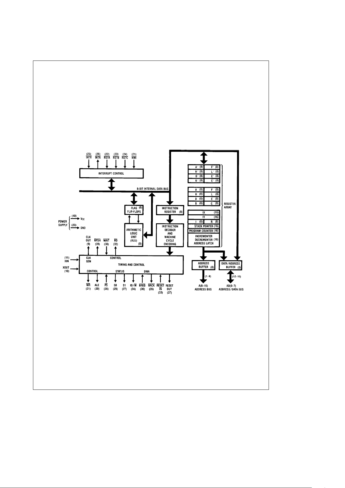
8.0 Functional Description
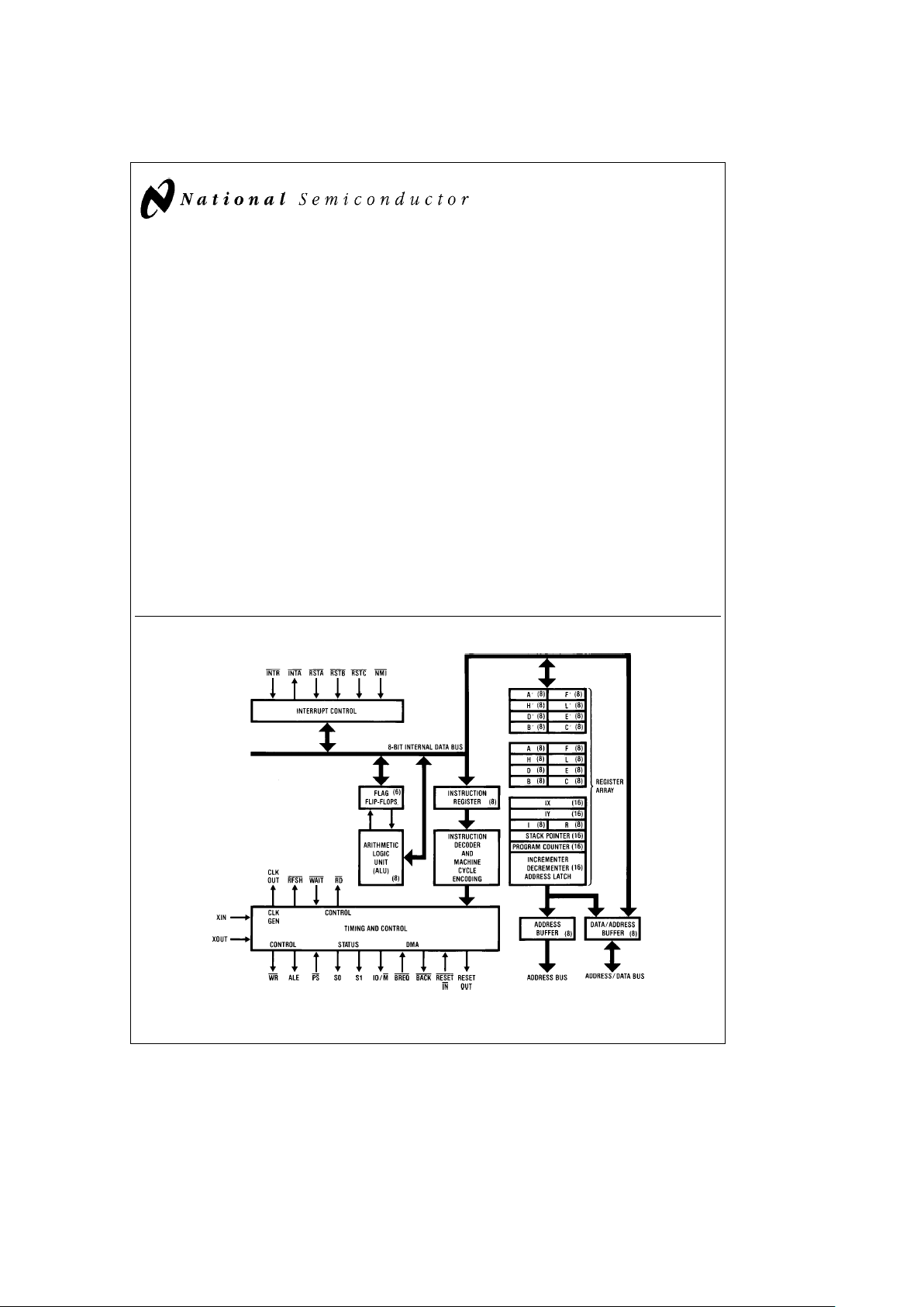
This section reviews the CPU architecture shown below, focusing on the functional aspects from a hardware perspective, including timing details.
As illustrated in
Figure 1
, the NSC800 is an 8-bit parallel
device. The major functional blocks are: the ALU, register
array, interrupt control, timing and control logic. These areas
are connected via the 8-bit internal data bus. Detailed descriptions of these blocks ae provided in the following sections.
TL/C/5171– 9
Note: Applicable pinout for 40-pin
dual-in-line package within parentheses
FIGURE 1. NSC800 CPU Functional Block Diagram
10
Page 11
8.0 Functional Description (Continued)
8.1 REGISTER ARRAY
The NSC800 register array is divided into two parts: the
dedicated registers and the working registers, as shown in
Figure 2
.
Main Reg. Set Alternate Reg. Set
V â WV â W
Accumulator Flags Accumulator Flags
AFA
Ê
F
Ê
BCB
Ê
C
Ê
Working
DED
Ê
E
Ê
Registers
HLH
Ê
L
Ê
*
Interrupt Memory
Vector I Refresh R
Index Register IX Dedicated
Index Register IY
Registers
Stack Pointer SP
Program Counter PC
–
FIGURE 2. NSC800 Register Array
8.2 DEDICATED REGISTERS
There are 6 dedicated registers in the NSC800: two 8-bit
and four 16-bit registers (see
Figure 3
).
Although their contents are under program control, the program has no control over their operational functions, unlike
the CPU working registers. The function of each dedicated
register is described as follows:
CPU Dedicated Registers
Program Counter PC (16)
Stack Pointer SP (16)
Index Register IX (16)
Index Register IY (16)
Interrupt Vector Register I (8)
Memory Refresh Register R (8)
FIGURE 3. Dedicated Registers
8.2.1 Program Counter (PC)
The program counter contains the 16-bit address of the current instruction being fetched from memory. The PC increments after its contents have been transferred to the address lines. When a program jump occurs, the PC receives
the new address which overrides the incrementer.
There are many conditional and unconditional jumps, calls,
and return instructions in the NSC800’s instruction repertoire that allow easy manipulation of this register in controlling the program execution (i.e. JP NZ nn, JR Zd2, CALL
NC, nn).
8.2.2 Stack Pointer (SP)
The 16-bit stack pointer contains the address of the current
top of stack that is located in external system RAM. The
stack is organized in a last-in, first-out (LIFO) structure. The
pointer decrements before data is pushed onto the stack,
and increments after data is popped from the stack.
Various operations store or retrieve, data on the stack. This,
along with the usage of subroutine calls and interrupts, allows simple implementation of subroutine and interrupt
nesting as well as alleviating many problems of data manipulation.
8.2.3 Index Register (IX and IY)
The NSC800 contains two index registers to hold independent, 16-bit base addresses used in the indexed addressing
mode. In this mode, an index register, either IX or IY, contains a base address of an area in memory making it a pointer for data tables.
In all instructions employing indexed modes of operation,
another byte acts as a signed two’s complement displacement. This addressing mode enables easy data table manipulations.
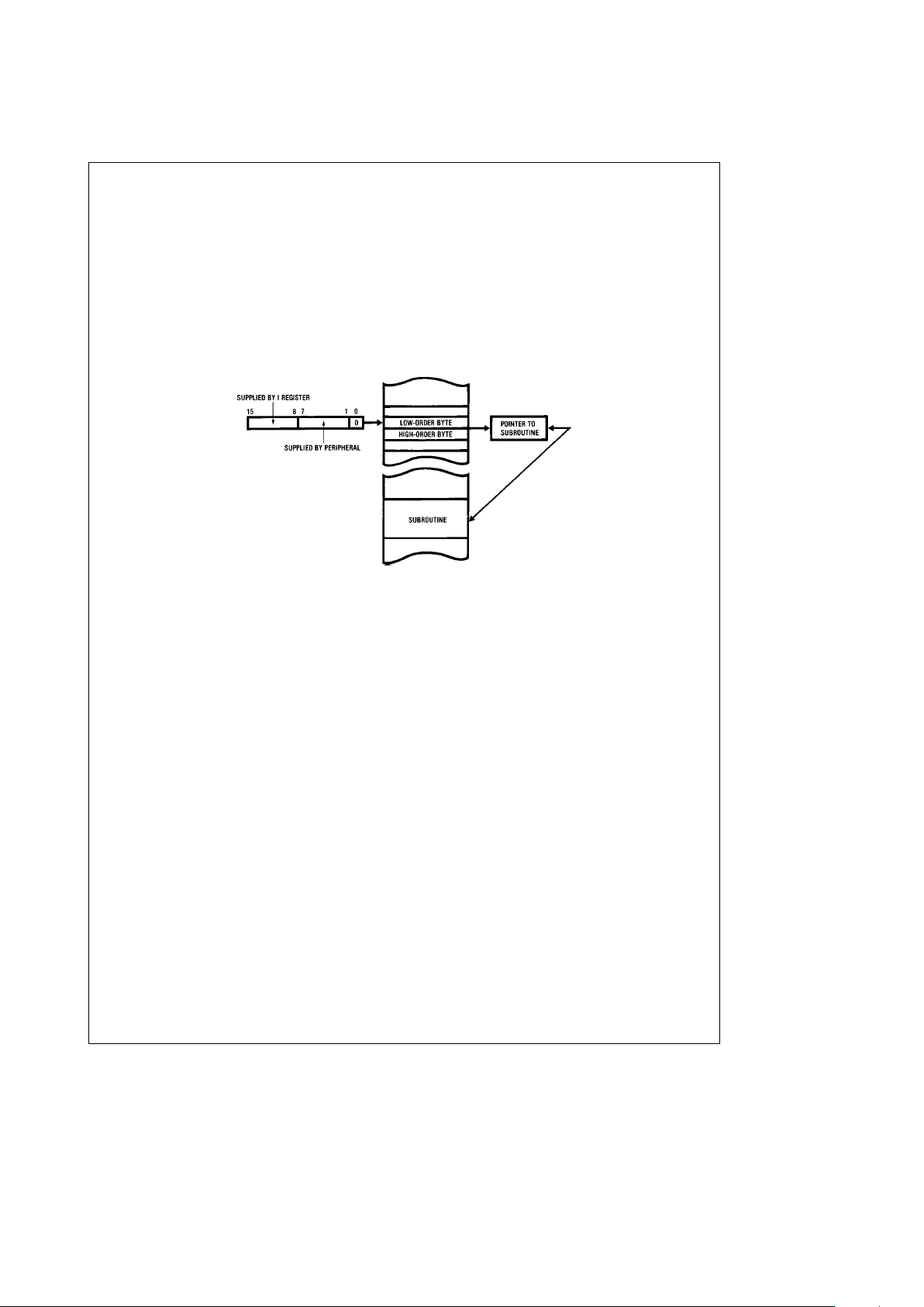
8.2.4 Interrupt Register (I)
When the NSC800 provides a Mode 2 response to INTR
,
the action taken is an indirect call to the memory location
containing the service routine address. The pointer to the
address of the service routine is formed by two bytes, the
high-byte is from the I Register and the low-byte is from the
interrupting peripheral. The peripheral always provides an
even address for the lower byte (LSB
e
0). When the processor receives the lower byte from the peripheral it concatenates it in the following manner:
I Register External byte
8 bits 0
u
The LSB of the external byte must be zero.
FIGURE 4a. Interrupt Register
The even memory location contains the low-order byte, the
next consecutive location contains the high-order byte of
the pointer to the beginning address of the interrupt service
routine.
8.2.5 Refresh Register (R)
For systems that use dynamic memories rather than static
RAM’s, the NSC800 provides an integral 8-bit memory refresh counter. The contents of the register are incremented
after each opcode fetch and are sent out on the lower portion of the address bus, along with a refresh control signal.
This provides a totally transparent refresh cycle and does
not slow down CPU operation.
The program can read and write to the R register, although
this is usually done only for test purposes.
11
Page 12
8.0 Functional Description (Continued)
8.3 CPU WORKING AND ALTERNATE REGISTER SETS
8.3.1 CPU Working Registers
The portion of the register array shown in
Figure 4b
represents the CPU working registers. These sixteen 8-bit registers are general-purpose registers because they perform a
multitude of functions, depending on the instruction being
executed. They are grouped together also due to the types
of instructions that use them, particularly alternate set operations.
The F (flag) register is a special-purpose register because
its contents are more a result of machine status rather than
program data. The F register is included because of its interaction with the A register, and its manipulations in the alternate register set operations.
8.3.2 Alternate Registers
The NSC800 registers designated as CPU working registers
have one common feature: the existence of a duplicate register in an alternate register set. This architectural concept
simplifies programming during operations such as interrupt
response, when the machine status represented by the contents of the registers must be saved.
The alternate register concept makes one set of registers
available to the programmer at any given time. Two instructions (EX AF, A‘F’ and EXX), exchange the current working
set of registers with their alternate set. One exchange between the A and F registers and their respective duplicates
(A’ and F’) saves the primary status information contained in
the accumulator and the flag register. The second exchange
instruction performs the exchange between the remaining
registers, B, C, D, E, H, and L, and their respective alternates B’, C’, D’, E’, H’, and L’. This essentially saves the
contents of the original complement of registers while providing the programmer with a usable alternate set.
CPU Main Working Register Set
Accumulator A (8) Flags F (8)
Register B (8) Register C (8)
Register D (8) Register E (8)
Register H (8) Register L (8)
CPU Alternate Working Register Set
Accumulator A’ (8) Flags F’ (8)
Register B’ (8) Register C’ (8)
Register D’ (8) Register E’ (8)
Register H’ (8) Register L’ (8)
FIGURE 4b. CPU Working and Alternate Registers
8.4 REGISTER FUNCTIONS
8.4.1 Accumulator (A Register)
The A register serves as a source or destination register for
data manipulation instructions. In addition, it serves as the
accumulator for the results of 8-bit arithmetic and logic operations.
The A register also has a special status in some types of
operations; that is, certain addressing modes are reserved
for the A register only, although the function is available for
all the other registers. For example, any register can be
loaded by immediate, register indirect, or indexed addressing modes. The A register, however, can also be loaded via
an additional register indirect addressing.
Another special feature of the A register is that it produces
more efficient memory coding than equivalent instruction
functions directed to other registers. Any register can be
rotated; however, while it requires a two-byte instruction to
normally rotate any register, a single-byte instruction is
available for rotating the contents of the accumulator (A register).
8.4.2 F Register - Flags
The NSC800 flag register consists of six status bits that
contain information regarding the results of previous CPU
operations. The register can be read by pushing the contents onto the stack and then reading it, however, it cannot
be written to. It is classified as a register because of its
affiliation with the accumulator and the existence of a duplicate register for use in exchange instructions with the accumulator.
Of the six flags shown in
Figure 5
, only four can be directly
tested by the programmer via conditional jump, call, and
return instructions. They are the Sign (S), Zero (Z), Parity/
Overflow (P/V), and Carry (C) flags. The Half Carry (H) and
Add/Subtract (N) flags are used for internal operations related to BCD arithmetic.
TL/C/5171– 23
FIGURE 5. Flag Register
12
Page 13

8.0 Functional Description (Continued)
8.4.3 Carry (C)
A carry from the highest order bit of the accumulator during
an add instruction, or a borrow generated during a subtraction instruction sets the carry flag. Specific shift and rotate
instructions also affect this bit.
Two specific instructions in the NSC800 instruction repertoire set (SCF) or complement (CCF) the carry flag.
Other operations that affect the C flag are as follows:
#
Adds
#
Subtracts
#
Logic Operations (always resets C flag)
#
Rotate Accumulator
#
Rotate and Shifts
#
Decimal Adjust
#
Negation of Accumulator
Other operations do not affect the C flag.
8.4.4 Adds/Subtract (N)
This flag is used in conjunction with the H flag to ensure that
the proper BCD correction algorithm is used during the decimal adjust instruction (DAA). The correction algorithm depends on whether an add or subtract was previously done
with BCD operands.
The operations that set the N flag are:
#
Subtractions
#
Decrements (8-bit)
#
Complementing of the Accumulator
#
Block I/O
#
Block Searches
#
Negation of the Accumulator
The operations that reset the N flag are:
#
Adds
#
Increments
#
Logic Operations
#
Rotates
#
Set and Complement Carry
#
Input Register Indirect
#
Block Transfers
#
Load of the I or R Registers
#
Bit Tests
Other operations do not affect the N flag.
8.4.5 Parity/Overflow (P/V)
The Parity/Overflow flag is a dual-purpose flag that indicates results of logic and arithmetic operations. In logic operations, the P/V flag indicates the parity of the result; the
flag is set (high) if the result is even, reset (low) if the result
is odd. In arithmetic operations, it represents an overflow
condition when the result, interpreted as signed two’s complement arithmetic, is out of range for the eight-bit accumulator (i.e.
b
128 toa127).
The following operations affect the P/V flag according to
the parity of the result of the operation:
#
Logic Operations
#
Rotate and Shift
#
Rotate Digits
#
Decimal Adjust
#
Input Register Indirect
The following operations affect the P/V flag according to
the overflow result of the operation.
#
Adds (16 bit with carry, 8-bit with/without carry)
#
Subtracts (16 bit with carry, 8-bit with/without carry)
#
Increments and Decrements
#
Negation of Accumulator
The P/V flag has no significance immediately after the following operations.
#
Block I/O
#
Bit Tests
In block transfers and compares, the P/V flag indicates the
status of the BC register, always ending in the reset state
after an auto repeat of a block move. Other operations do
not affect the P/V flag.
8.4.6 Half Carry (H)
This flag indicates a BCD carry, or borrow, result from the
low-order four bits of operation. It can be used to correct the
results of a previously packed decimal add, or subtract, operation by use of the Decimal Adjust Instruction (DAA).
The following operations affect the H flag:
#
Adds (8-bit)
#
Subtracts (8-bit)
#
Increments and Decrements
#
Decimal Adjust
#
Negation of Accumulator
#
Always Set by: Logic AND
Complement Accumulator
Bit Testing
#
Always Reset By: Logic OR’s and XOR’s
Rotates and Shifts
Set Carry
Input Register Indirect
Block Transfers
Loads of I and R Registers
The H flag has no significance immediately after the following operations.
#
16-bit Adds with/without carry
#
16-Bit Subtracts with carry
#
Complement of the carry
#
Block I/O
#
Block Searches
Other operations do not affect the H flag.
13
Page 14

8.0 Functional Description (Continued)
8.4.7 Zero Flag (Z)
Loading a zero in the accumulator or when a zero results
from an operation sets the zero flag.
The following operations affect the zero flag.
#
Adds (16-bit with carry, 8-bit with/without carry)
#
Subtracts (16-bit with carry, 8-bit with/without carry)
#
Logic Operations
#
Increments and Decrements
#
Rotate and Shifts
#
Rotate Digits
#
Decimal Adjust
#
Input Register Indirect
#
Block I/O (always set after auto repeat block I/O)
#
Block Searches
#
Load of I and R Registers
#
Bit Tests
#
Negation of Accumulator
The Z flag has no signficance immediately after the following operations:
#
Block Transfers
Other operations do not affect the zero flag.
8.4.8 Sign Flag (S)
The sign flag stores the state of bit 7 (the most-significant bit and sign bit) of the accumulator following an arithmetic operation. This flag is of use when dealing with signed
numbers.
The sign flag is affected by the following operation according to the result:
#
Adds (16-bit with carry, 8-bit with/without carry)
#
Subtracts (16-bit with carry, 8-bit with/without carry)
#
Logic Operations
#
Increments and Decrements
#
Rotate and Shifts
#
Rotate Digits
#
Decimal Adjust
#
Input Register Indirect
#
Block Search
#
Load of I and R Registers
#
Negation of Accumulator
The S flag has no significance immediately after the following operations:
#
Block I/O
#
Block Transfers
#
Bit Tests
Other operations do not affect the sign bit.
8.4.9 Additional General-Purpose Registers
The other general-purpose registers are the B, C, D, E, H
and L registers and their alternate register set, B’, C’, D’, E’,
H’ and L’. The general-purpose registers can be used interchangeably.
In addition, the B and C registers perform special functions
in the NSC800 expanded I/O capabilities, particularly block
I/O operations. In these functions, the C register can address I/O ports; the B register provides a counter function
when used in the register indirect address mode.
When used with the special condition jump instruction
(DJNZ) the B register again provides the counter function.
8.4.10 Alternate Configurations
The six 8-bit general purpose registers (B,C,D,E,H,L) will
combine to form three 16-bit registers. This occurs by concatenating the B and C registers to form the BC register, the
D and E registers form the DE register, and the H and L
registers form the HL register.
Having these 16-bit registers allows 16-bit data handling,
thereby expanding the number of 16-bit registers available
for memory addressing modes. The HL register typically
provides the pointer address for use in register indirect addressing of the memory.
The DE register provides a second memory pointer register
for the NSC800’s powerful block transfer operations. The
BC register also provides an assist to the block transfer
operations by acting as a byte-counter for these operations.
8.5 ARITHMETIC-LOGIC UNIT (ALU)
The arithmetic, logic and rotate instructions are performed
by the ALU. The ALU internally communicates with the registers and data buffer on the 8-bit internal data bus.
8.6 INSTRUCTION REGISTER AND DECODER
During an opcode fetch, the first byte of an instruction is
transferred from the data buffer (i.e. its on the internal data
bus) to the instruction register. The instruction register feeds
the instruction decoder, which gated by timing signals, generates the control signals that read or write data from or to
the registers, control the ALU and provide all required external control signals.
14
Page 15
9.0 Timing and Control
9.1 INTERNAL CLOCK GENERATOR
An inverter oscillator contained on the NSC800 chip provides all necessary timing signals. The chip operation frequency is equal to one half of the frequency of this oscillator.
The oscillator frequency can be controlled by one of the
following methods:
1. Leaving the X
OUT
pin unterminated and driving the X
IN
pin with an externally generated clock as shown in
Figure
6
. When driving XINwith a square wave, the minimum
duty cycle is 30% high.
TL/C/5171– 13
FIGURE 6. Use of External Clock
2. Connecting a crystal with the proper biasing network between X
IN
and X
OUT
as shown in
Figure 7
. Recommend-
ed crystal is a parallel resonance AT cut crystal.
Note 1: If the crystal frequency is between 1 MHz and 2 MHz a series
resistor, R
S
, (470X to 1500X) should be connected between
X
OUT
and R, XTAL and CZ. Additionally, the capacitance of C1
and C2 should be increased by 2 to 3 times the recommended
value. For crystal frequencies less than 1 MHz higher values of
C1 and C2 may be required. Crystal parameters will also affect
the capacitive loading requirements.
2 MHz
k
f(XTAL)
2
R
e
1MX
C1
e
20 pF
C2
e
34 pF
(Recommended)
TL/C/5171– 14
FIGURE 7. Use Of Crystal
The CPU has a minimum clock frequency input (@XIN)of
300 kHz, which results in 150 kHz system clock speed. All
registers internal to the chip are static, however there is
dynamic logic which limits the minimum clock speed. The
input clock can be stopped without fear of losing any data or
damaging the part. You stop it in the phase of the clock that
has X
IN
low and CLK OUT high. When restarting the CPU,
precautions must be taken so that the input clock meets
these minimum specification. Once started, the CPU will
continue operation from the same location at which it was
stopped. During DC operation of the CPU, typical current
drain will be 2 mA. This current drain can be reduced by
placing the CPU in a wait state during an opcode fetch cycle
then stopping the clock. For clock stop circuit, see
Figure 8
.
TL/C/5171– 36
FIGURE 8. Clock Stop Circuit
15
Page 16
9.0 Timing and Control (Continued)
9.2 CPU TIMING
The NSC800 uses a multiplexed bus for data and addresses. The 16-bit address bus is divided into a high-order 8-bit
address bus that handles bits 8 – 15 of the address, and a
low-order 8-bit multiplexed address/data bus that handles
bits 0 – 7 of the address and bits 0 –7 of the data. Strobe
outputs from the NSC800 (ALE, RD
and WR) indicate when
a valid address or data is present on the bus. IO/M
indi-
cates whether the ensuing cycle accesses memory or I/O.
During an input or output instruction, the CPU duplicates the
lower half of the address[AD(0–7)]onto the upper address
bus[A(8–15)]. The eight bits of address will stay on A(8 –
15) for the entire machine cycle and can be used for chip
selection directly.
Figure 9
illustrates the timing relationship for opcode fetch
cycles with and without a wait state.
TL/C/5171– 15
FIGURE 9a. Opcode Fetch Cycles without WAIT
States
TL/C/5171– 16
FIGURE 9b. Opcode Fetch Cycles with WAIT States
16
Page 17
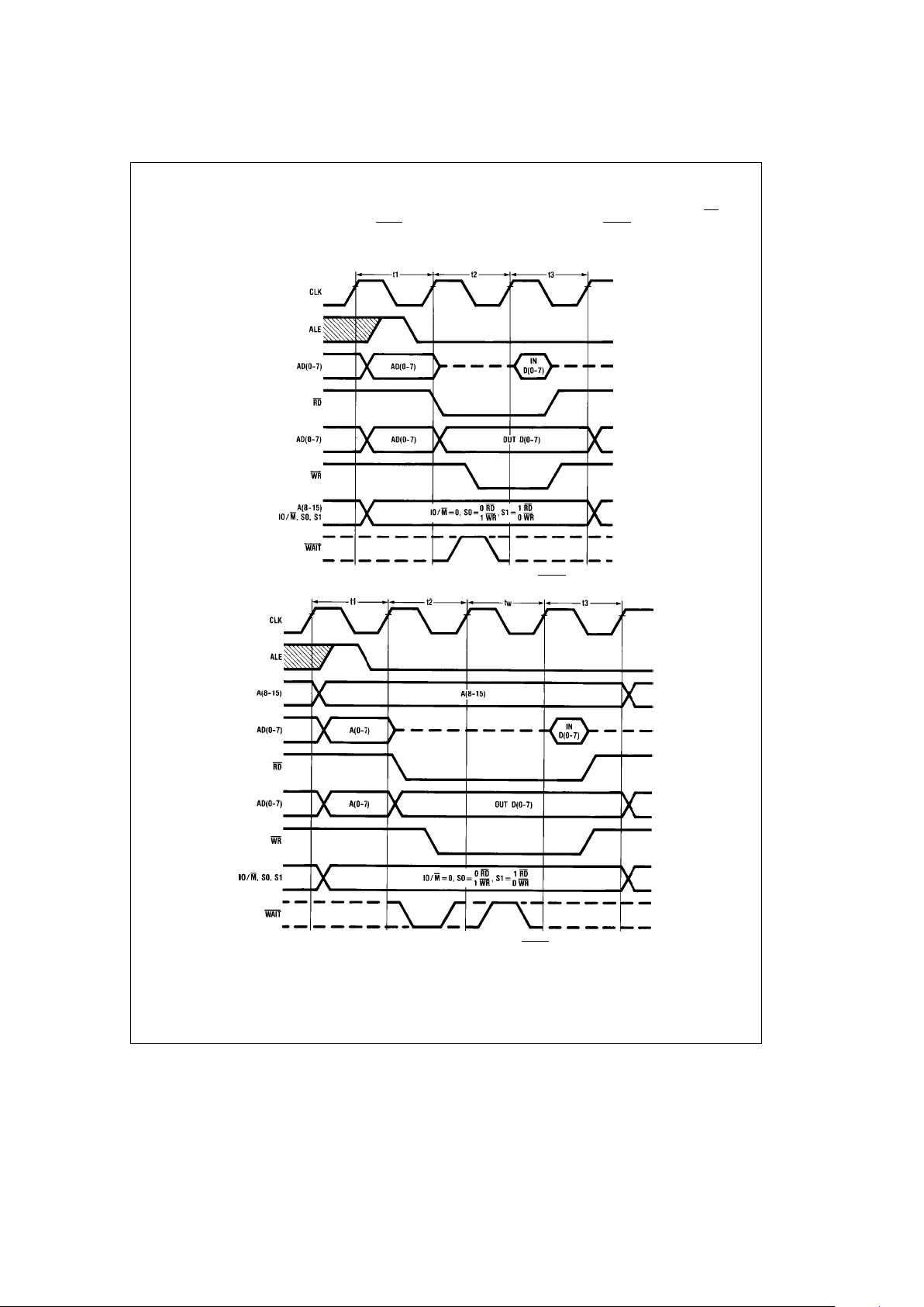
9.0 Timing and Control (Continued)
During the opcode fetch, the CPU places the contents of
the PC on the address bus. The falling edge of ALE indicates a valid address on the AD(0 –7) lines. The WAIT
input
is sampled during t
2
and if active causes the NSC800 to
insert a wait state (t
w
). WAIT is sampled again during twso
that when it goes inactive, the CPU continues its opcode
fetch by latching in the data on the rising edge of RD
from
the AD(0 – 7) lines. During t
3
, RFSH goes active and AD(0–
7) has the dynamic RAM refresh address from register R
and A(8 – 15) the interrupt vector from register I.
TL/C/5171– 17
FIGURE 10a. Memory Read/Write Cycles without WAIT States
TL/C/5171– 18
FIGURE 10b. Memory Read and Write with WAIT States
17
Page 18
9.0 Timing and Control (Continued)
Figure 10
shows the timing for memory read (other than
opcode fetchs) and write cycles with and without a wait
state. The RD
stobe is widened by
t
2
(half the machine
state) for memory reads so that the actual latching of the
input data occurs later.
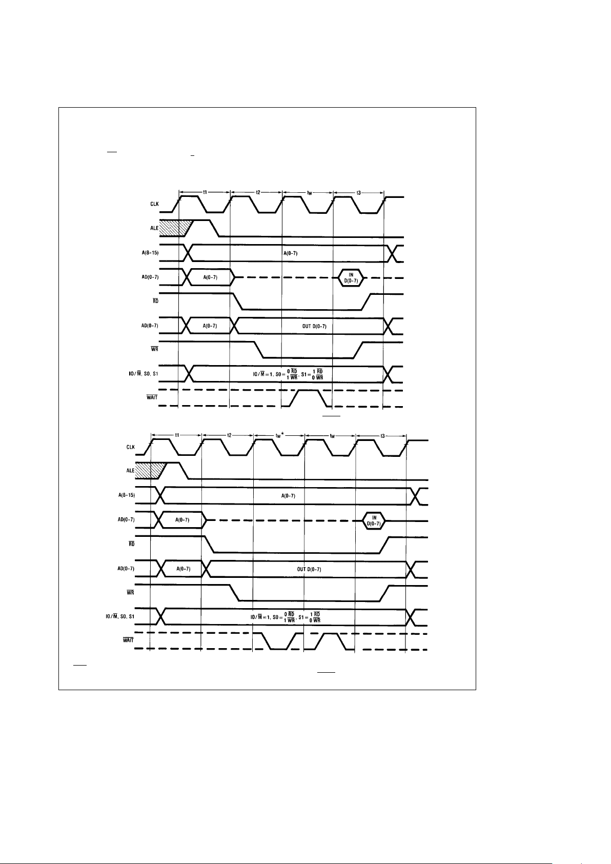
Figure 11
shows the timing for input and output cycles with
and without wait states. The CPU automatically inserts one
wait state into each I/O instruction to allow sufficient time
for an I/O port to decode the address.
TL/C/5171– 19
FIGURE 11a. Input and Output Cycles without WAIT States
TL/C/5171– 20
*WAIT state automatically inserted during IO operation.
FIGURE 11b. Input and Output Cycles with WAIT States
18
Page 19
9.0 Timing and Control (Continued)
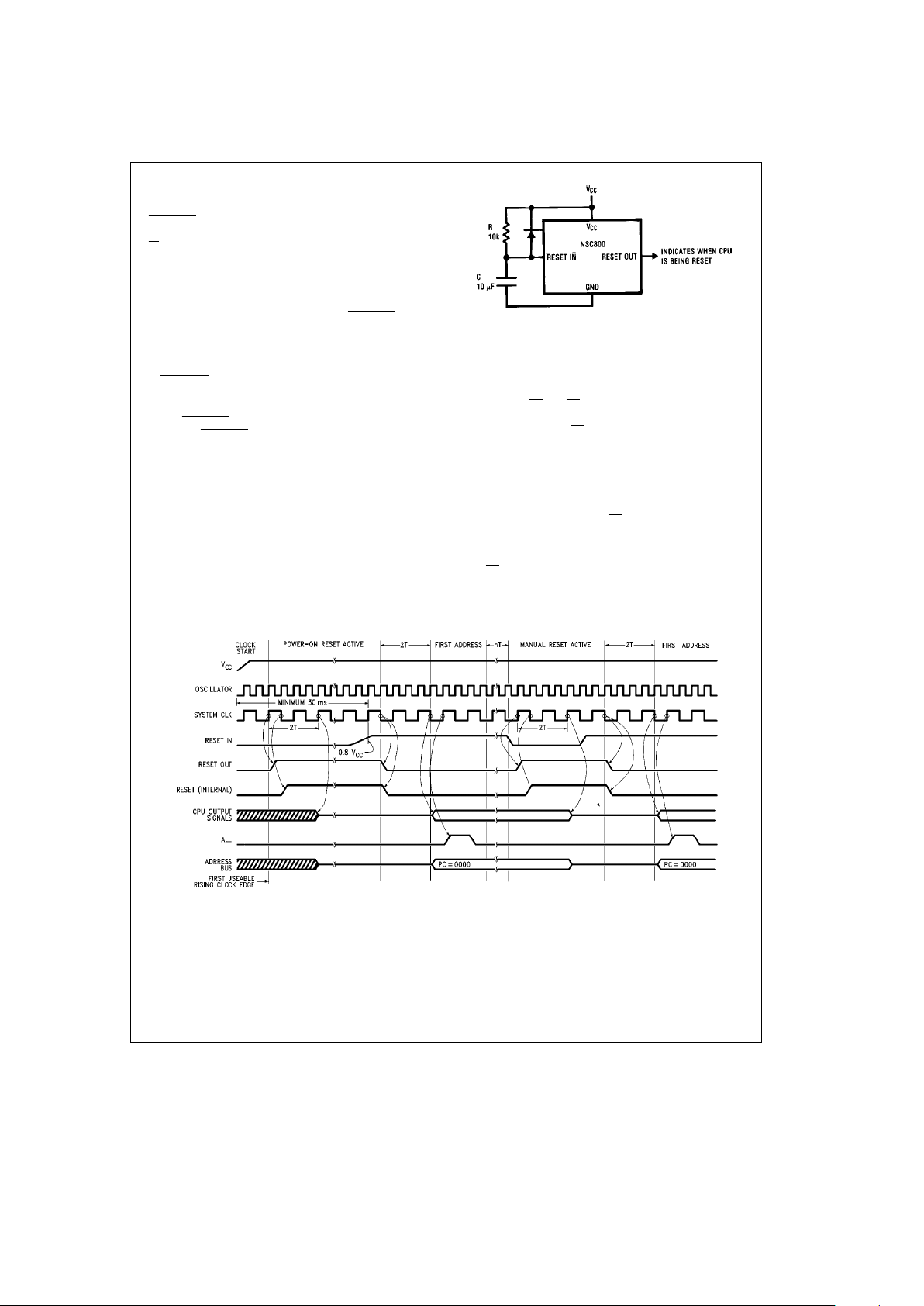
9.3 INITIALIZATION
RESET IN
initializes the NSC800; RESET OUT initializes the
peripheral components. The Schmitt trigger at the RESET
IN input facilitates using an R-C network reset scheme during power up (see
Figure 12
).
To ensure proper power-up conditions for the NSC800, the
following power-up and initialization procedure is recommended:
1. Apply power (V
CC
and GND) and set RESET IN active
(low). Allow sufficient time (approximately 30 ms if a crystal is used) for the oscillator and internal clocks to stabilize. RESET IN
must remain low for at least 3t state (CLK)
times. RESET OUT goes high as soon as the active
RESET IN
signal is clocked into the first flip-flop after the
on-chip Schmitt trigger. RESET OUT signal is available to
reset the peripherals.
2. Set RESET IN
high. RESET OUT then goes low as the
inactive RESET IN
signal is clocked into the first flip-flop
after the on-chip Schmitt trigger. Following this the CPU
initiates the first opcode fetch cycle.
Note: The NSC800 initialization includes: Clear PC to
X’0000 (the first opcode fetch, therefore, is from memory
location X’0000). Clear registers I (Interrupt Vector Base)
and R (Refresh Counter) to X’00. Clear interrupt control register bits IEA, IEB and IEC. The interrupt control bit IEI is set
to 1 to maintain INS8080A/Z80A compatibility (see INTERRUPTS for more details). The CPU disables maskable interrupts and enters INTR
Mode 0. While RESET IN is active
(low), the A(8 – 15) and AD(0–7) lines go to high impedance
(TRI-STATE) and all CPU strobes go to the inactive state
(see
Figure 13
).
TL/C/5171– 21
FIGURE 12. Power-On Reset
9.4 POWER-SAVE FEATURE
The NSC800 provides a unique power-save mode by the
means of the PS
pin. PS input is sampled at the last t state
of the last M cycle of an instruction. After recognizing an
active (low) level on PS
, The NSC800 stops its internal
clocks, thereby reducing its power dissipation to one half of
operating power, yet maintaining all register values and internal control status. The NSC800 keeps its oscillator running, and makes the CLK signal available to the system.
When in power-save the ALE strobe will be stopped high
and the address lines[AD(0–7), A(8 – 15)]will indicate the
next machine address. When PS
returns high, the opcode
fetch (or M1 cycle) of the CPU begins in a normal manner.
Note this M1 cycle could also be an interrupt acknowledge
cycle if the NSC800 was interrupted simultaneously with PS
(i.e. PS has priority over a simultaneously occurring interrupt). However, interrupts are not accepted during power
save.
Figure 14
illustrates the power save timing.
TL/C/5171– 74
FIGURE 13. NSC800 Signals During Power-On and Manual Reset
19
Page 20
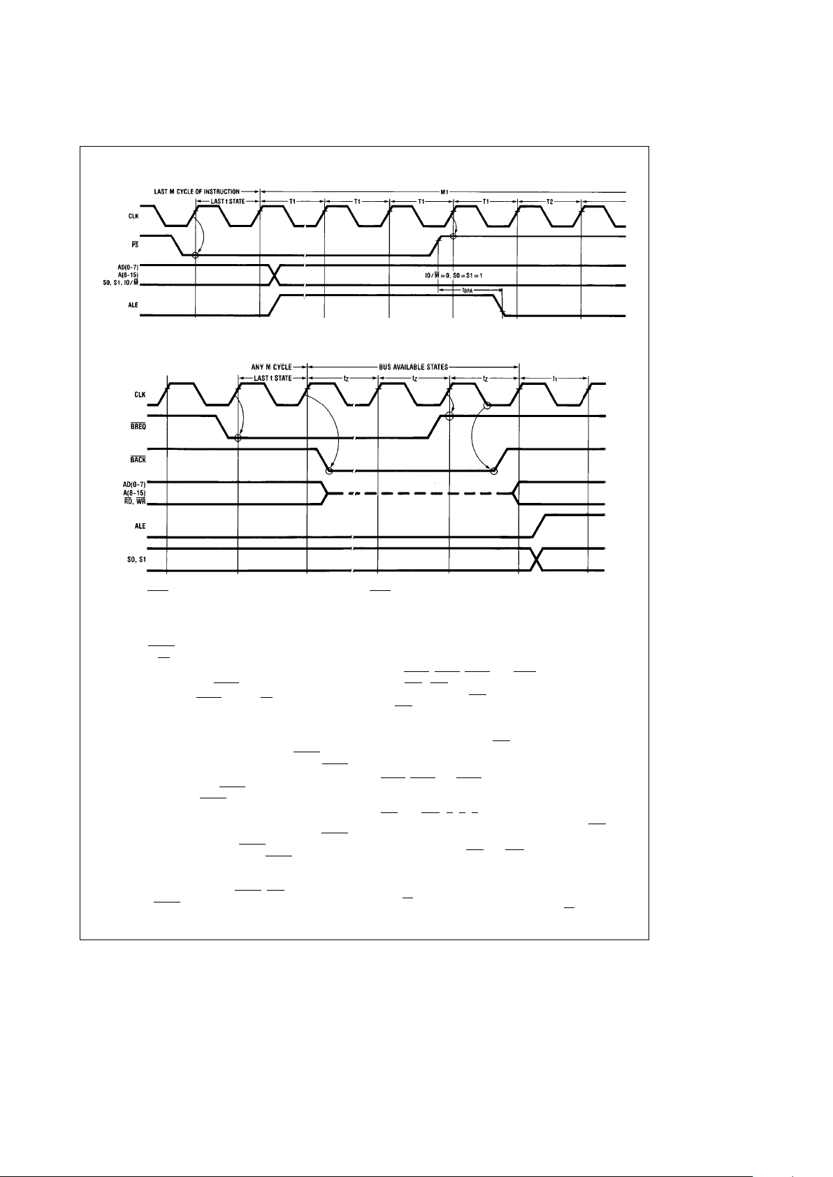
9.0 Timing and Control (Continued)
TL/C/5171– 28
FIGURE 14. NSC800 Power-Save
TL/C/5171– 22
*S0, S1 during BREQ will indicate same machine cycle as during the cycle when BREQ was accepted.
t
Z
e
time states during which bus and control signals are in high impedance mode.
FIGURE 15. Bus Acknowledge Cycle
In the event BREQ
is asserted (low) at the end of an instruc-
tion cycle and PS
is active simultaneously, the following oc-
curs:
1. The NSC800 will go into BACK
cycle.
2. Upon completion of BACK cycle if PS is still active the
CPU will go into power-save mode.
9.5 BUS ACCESS CONTROL
Figure 15
illustrates bus access control in the NSC800. The
external device controller produces an active BREQ
signal
that requests the bus. When the CPU responds with BACK
then the bus and related control strobes go to high impedance (TRI-STATE) and the RFSH
signal remains high. It
should be noted that (1) BREQ
is sampled at the last t state
of any M machine cycle only. (2) The NSC800 will not acknowledge any interrupt/restart requests, and will not peform any dynamic RAM refresh functions until after BREQ
input signal is inactive high. (3) BREQ signal has priority
over all interrupt request signals, should BREQ
and interrupt
request become active simultaneously. Therefore, interrupts
latched at the end of the instruction cycle will be serviced
after a simultaneously occurring BREQ
. NMI is latched dur-
ing an active BREQ
.
9.6 INTERRUPT CONTROL
The NSC800 has five interrupt/restart inputs, four are maskable (RSTA
, RSTB, RSTC, and INTR) and one is non-mask-
able (NMI
). NMI has the highest priority of all interrupts; the
user cannot disable NMI
. After recognizing an active input
on NMI
, the CPU stops before the next instruction, pushes
the PC onto the stack, and jumps to address X’0066, where
the user’s interrupt service routine is located (i.e., restart to
memory location X’0066). NMI
is intended for interrupts requiring immediate attention, such as power-down, control
panel, etc.
RSTA
, RSTB and RSTC are restart inputs, which, if enabled,
execute a restart to memory location X’003C, X’0034, and
X’002C, respectively. Note that the CPU response to the
NMI
and RST (A,B,C) request input is basically identical,
except for the restored memory location. Unlike NMI
, how-
ever, restart request inputs must be enabled.
Figure 16
illustrates NMI and RST interrupt machine cycles.
M1 cycle will be a dummy opcode fetch cycle followed by
M2 and M3 which are stack push operations. The following
instruction then starts from the interrupts restart location.
Note: RD does
not
go low during this dummy opcode fetch. A unique indica-
tion of INTA can be decoded using 2 ALEs and RD
.
20
Page 21
9.0 Timing and Control (Continued)
TL/C/5171– 24
Note 1: This is the only machine cycle that does not have an RD,WR, or INTA strobe but will accept a wait strobe.
FIGURE 16. Non-Maskable and Restart Interrupt Machine Cycle
The NSC800 also provides one more general purpose interrupt request input, INTR
. When enabled, the CPU responds
to INTR
in one of the three modes defined by instruction
IM0, IM1, and IM2 for modes 0, 1, and 2, respectively. Following reset, the CPU automatically enables mode 0.
Interrupt (INTR
) Mode 0: The CPU responds to an interrupt
request by providing an INTA (interrupt acknowledge)
strobe, which can be used to gate an instruction from a
peripheral onto the data bus. The CPU inserts two wait
states during the first INTA
cycle to allow the interrupting
device (or its controller) ample time to gate the instruction
and determine external priorities (
Figure 18
). This can be
any instruction from one to four bytes. The most popular
instruction is one-byte call (restart instruction) or a threebyte call (CALL NN instruction). If it is a three-byte call, the
CPU issues a total of three INTA
strobes. The last two
(which do not include wait states) read NN.
Note: If the instruction stored in the ICU doesn’t require the PC to be
pushed onto the stack (eq. JP nn), then the PC will not be pushed.
Interrupt (INTR) Mode 1: Similar to restart interrupts except the restart location is X’0038 (
Figure 18
).
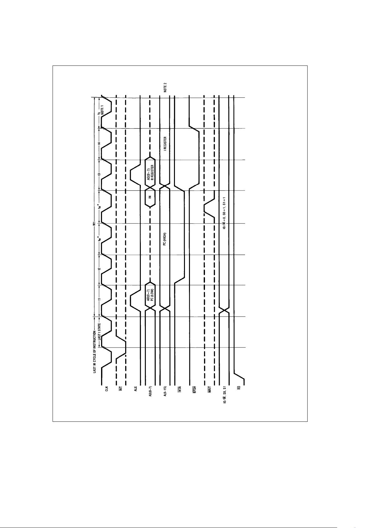
Interrupt (INTR
) Mode 2: With this mode, the programmer
maintains a table that contains the 16-bit starting address of
every interrupt service routine. This table can be located
anywhere in memory. When the CPU accepts a Mode 2
interrupt (
Figure 17
), it forms a 16-bit pointer to obtain the
desired interrupt service routine starting address from the
table. The upper 8 bits of this pointer are from the contents
of the I register. The lower 8 bits of the pointer are supplied
by the interrupting device with the LSB forced to zero. The
programmer must load the interrupt vector prior to the interrupt occurring. The CPU uses the pointer to get the two
adjacent bytes from the interrupt service routine starting address table to complete 16-bit service routine starting ad-
dress. The first byte of each entry in the table is the least
significant (low-order) portion of the address. The programmer must obviously fill this table with the desired addresses
before any interrupts are to be accepted.
Note that the programmer can change this table at any time
to allow peripherals to be serviced by different service routines. Once the interrupting device supplies the lower portion of the pointer, the CPU automatically pushes the program counter onto the stack, obtains the starting address
from the table and does a jump to this address.
The interrupts have fixed priorities built into the NSC800 as:
NMI
0066 (Highest Priority)
RSTA
003C
RSTB
0034
RSTC
002C
INTR
0038 (Lowest Priority)
Interrupt Enable, Interrupt Disable. The NSC800 has two
types of interrupt inputs, a non-maskable interrupt and four
software maskable interrupts. The non-maskable interrupt
(NMI
) cannot be disabled by the programmer and will be
accepted whenever a peripheral device requests an interrupt. The NMI
is usually reserved for important functions
that must be serviced when they occur, such as imminent
power failure. The programmer can selectively enable or
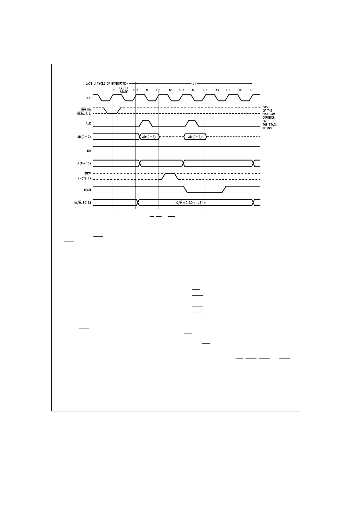
disable maskable interrupts (INT
, RSTA, RSTB and RSTC).
This selectivity allows the programmer to disable the maskable interrupts during periods when timing constraints don’t
allow program interruption.
There are two interrupt enable flip-flops (IFF
1
and IFF2)on
the NSC800. Two instructions control these flip-flops. Enable Interrupt (EI) and Disable Interrupt (DI). The state of
IFF
1
determines the enabling or disabling of the maskable
interrupts, while IFF
2
is used as a temporary storage loca-
tion for the state of IFF
1
.
21
Page 22
9.0 Timing and Control (Continued)
A reset to the CPU will force both IFF
1
and IFF2to the reset
state disabling maskable interrupts. They can be enabled by
an EI instruction at any time by the programmer. When an EI
instruction is executed, any pending interrupt requests will
not be accepted until after the instruction following EI has
been executed. This single instruction delay is necessary in
situations where the following instruction is a return instruction and interrupts must not be allowed until the return has
been completed. The EI instruction sets both IFF
1
and IFF
2
to the enable state. When the CPU accepts an interrupt,
both IFF
1
and IFF2are automatically reset, inhibiting further
interrupts until the programmer wishes to issue a new EI
instruction. Note that for all the previous cases, IFF
1
and
IFF
2
are always equal.
The function of IFF
2
is to retain the status of IFF1when a
non-maskable interrupt occurs. When a non-maskable interrupt is accepted, IFF
1
is reset to prevent further interrupts
until reenabled by the programmer. Thus, after a non-maskable interrupt has been accepted, maskable interrupts are
disabled but the previous state of IFF
1
is saved by IFF
2
TL/C/5171– 27
FIGURE 17. Interrupt Mode 2
22
Page 23
9.0 Timing and Control (Continued)
TL/C/5171– 25
*t
W
is the CPU generated WAIT state in response to an interrupt request.
Note 1: t5 will only occur in mode 1 and mode 2. During t5 the stack pointer is decremented.
Note 2: A jump to the appropriate address occurs here in mode 1 and mode 2. The CPU continues gathering data from the interrupting peripheral in mode 0 for a total of 2 –4
machine cycles. In mode 0 cycles M2 –M4 have only 1 wait state.
FIGURE 18. Interrupt Acknowledge Machine Cycle
23
Page 24

9.0 Timing and Control (Continued)
so that the complete state of the CPU just prior to the nonmaskable interrupt may be restored. The method of restoring the status of IFF
1
is through the execution of a Return
Non-Maskable Interrupt (RETN) instruction. Since this instruction indicates that the non-maskable interrupt service
routine is completed, the contents of IFF
2
are now copied
back into IFF
1
, so that the status of IFF1just prior to the
acceptance of the non-maskable interrupt will be automatically restored.
Figure 19
depicts the status of the flip flops during a sample
series of interrupt instructions.
Interrupt Control Register. The interrupt control register
(ICR) is a 4-bit, write only register that provides the programmer with a second level of maskable control over the four
maskable interrupt inputs.
The ICR is internal to the NSC800 CPU, but is addressed
through the I/O space at I/O address port X’BB. Each bit in
the register controls a mask bit dedicated to each maskable
interrupt, RSTA
, RSTB, RSTC and INTR. For an interrupt
request to be accepted on any of these inputs, the corresponding mask bit in the ICR must be set (
e
1) and IFF
1
and IFF2must be set. This provides the programmer with
control over individual interrupt inputs rather than just a system wide enable or disable.
TL/C/5171– 26
Bit Name Function
0 IEI Interrupt Enable for INTR
1 IEC Interrupt Enable for RSTC
2 IEB Interrupt Enable for RSTB
3 IEA Interrupt Enable for RSTA
For example: In order to enable RSTB, CPU interrupts must
be enabled and IEB must be set.
At reset, IEI bit is set and other mask bits IEA, IEB, IEC are
cleared. This maintains the software compatibility between
NSC800 and Z80A.
Execution of an I/O block move instruction will not affect
the state of the interrupt control bits. The only two instructions that will modify this write only register are OUT (C), r
and OUT (N), A.
Operation IFF1IFF
2
Comment
Initialize 0 0 Interrupt Disabled
#
#
#
EI 1 1 Interrupt Enabled after
#
next instruction
#
#
INTR 0 0 Interrupt Disable and INTR
Being Serviced
#
#
#
EI 1 1 Interrupt Enabled after
next instruction
RET 1 1 Interrupt Enabled
#
#
#
NMI 0 1 Interrupt Disabled
#
#
#
RETN 1 1 Interrupt Enabled
#
INTR 0 0 Interrupt Disabled
#
#
#
NMI 0 0 Interrupt Disabled and NMI
#
Being Serviced
#
#
RETN 0 0 Interrupt Disabled and INTR
#
Being Serviced
#
#
EI 1 1 Interrupt Enabled after
next instruction
RET 1 1 Interrupt Enabled
#
#
#
FIGURE 19. IFF1and IFF2States Immediately after the
Operation has been Completed
24
Page 25

NSC800 SOFTWARE
10.0 Introduction
This chapter provides the reader with a detailed description
of the NSC800 software. Each NSC800 instruction is described in terms of opcode, function, flags affected, timing,
and addressing mode.
11.0 Addressing Modes
The following sections describe the addressing modes supported by the NSC800. Note that particular addressing
modes are often restricted to certain types of instructions.
Examples of instructions used in the particular addressing
modes follow each mode description.
The 10 addressing modes and 158 instructions provide a
flexible and powerful instruction set.
11.1 REGISTER
The most basic addressing mode is that which addresses
data in the various CPU registers. In these cases, bits in the
opcode select specific registers that are to be addressed by
the instruction.
Example:
Instruction: Load register B from register C
Mnemonic: LD B,C
Opcode:
TL/C/5171– 50
In this instruction, both the B and C registers are addressed
by opcode bits.
11.2 IMPLIED
The implied addressing mode is an extension to the register
addressing mode. In this mode, a specific register, the accumulator, is used in the execution of the instruction. In particular, arithmetic operations employ implied addressing, since
the A register is assumed to be the destination register for
the result without being specifically referenced in the opcode.
Example:
Instruction: Subtract the contents of register D from the
Accumulator (A register)
Mnemonic: SUB D
Opcode:
TL/C/5171– 51
In this instruction, the D register is addressed with register
addressing, while the use of the A register is implied by the
opcode.
11.3 IMMEDIATE
The most straightforward way of introducing data to the
CPU registers is via immediate addressing, where the data
is contained in an additional byte of multi-byte instructions.
Example:
Instruction: Load the E register with the constant value
X’7C.
Mnemonic: LD E,X’7C
Opcode:
TL/C/5171– 52
In this instruction, the E register is addressed with register
addressing, while the constant X’7C is immediate data in the
second byte of the instruction.
11.4 IMMEDIATE EXTENDED
As immediate addressing allows 8 bits of data to be supplied by the operand, immediate extended addressing allows 16 bits of data to be supplied by the operand. These
are in two additional bytes of the instruction.
Example:
Instruction: Load the 16-bit IX register with the constant
value X’ABCD.
Mnemonic: LD IX,X’ABCD
Opcode:
TL/C/5171– 53
In this instruction, register addressing selects the IX register, while the 16-bit quanity X’ABCD is immediate data supplied as immediate extended format.
25
Page 26

11.0 Addressing Modes (Continued)
11.5 DIRECT ADDRESSING
Direct addressing is the most straightforward way of addressing supplies a location in the memory space. Direct
addressing, 16-bits of memory address information in two
bytes of data as part of the instruction. The memory address
could be either data, source of destination, or a location for
program execution, as in program control instructions.
Example:
Instruction: Jump to location X’0377
Mnemonic: JP X’0377
Opcode:
11000011 ÐDefines jump opcode
01110111
ÐConstant X’0377
00000011(
This instruction loads the Program Counter (PC) is loaded
with the constant in the second and third bytes of the instruction. The program counter contents are transferred via
direct addressing.
11.6 REGISTER INDIRECT
Next to direct addressing, register indirect addressing provides the second most straightforward means of addressing
memory. In register indirect addressing, a specified register
pair contains the address of the desired memory location.
The instruction references the register pair and the register
contents define the memory location of the operand.
Example:
Instruction: Add the contents of memory location X’0254 to
the A register. The HL register contains X’0254.
Mnemonic: ADD A,(HL)
Opcode
10000110
This instruction uses implied addressing of the A and HL
registers and register indirect addressing to access the data
pointed to by the HL register.
11.7 INDEXED
The most flexible mode of memory addressing is the indexed mode. This is similar to the register indirect mode of
addressing because one of the two index registers (IX or IY)
contains the base memory address. In addition, a byte of
data included in the instruction acts as a displacement to
the address in the index register.
Indexed addressing is particularly useful in dealing with lists
of data.
Example:
Instruction: Increment the data in memory location X’1020.
The IY register contains X’1000.
Mnemonic: INC (IY
a
X’20)
Opcode:
TL/C/5171– 54
The indexed addressing mode uses the contents of index
registers IX or IY along with the displacement to form a
pointer to memory.
11.8 RELATIVE
Certain instructions allow memory locations to be addressed as a position relative to the PC register. These instructions allow jumps to memory locations which are offsets around the program counter. The offset, together with
the current program location, is determined through a displacement byte included in the instruction. The formation of
this displacement byte is explained more fully in the ‘‘Instructions Set’’ section.
Example:
Instruction: Jump to a memory location 7 bytes beyond the
current location.
Mnemonic: JR $
a
7
Opcode:
00011000ÐDefines relative jump
opcode
00000101ÐDisplacement to be
applied to the PC
The program will continue at a location seven locations past
the current PC.
26
Page 27

11.0 Addressing Modes (Continued)
11.9 MODIFIED PAGE ZERO
A subset of NSC800 instructions (the Restart instructions)
provides a code-efficient single-byte instruction that allows
CALLs to be performed to any one of eight dedicated locations in page zero (locations X’0000 to X’00FF). Normally, a
CALL is a 3-byte instruction employing direct memory addressing.
Example:
Instruction: Perform a restart call to location X’0028.
Mnemonic: RST X’28
Opcode:
TL/C/5171– 55
p 00H 08H 10H 18H 20H 28H 30H 38H
t 000 001 010 011 100 101 110 111
Program execution continues at location X’0028 after execution of a single-byte call employing modified page zero
addressing.
11.10 BIT
The NSC800 allows setting, resetting, and testing of individual bits in registers and memory data bytes.
Example:
Operation: Set bit 2 in the L register
Mnemonic: SET 2,L
Opcode:
TL/C/5171– 56
Bit addressing allows the selection of bit 2 in the L register
selected by register addressing.
27
Page 28

12.0 Instruction Set
This section details the entire NSC800 instruction set in
terms of
#
Opcode
#
Instruction
#
Function
#
Timing
#
Addressing Mode
The instructions are grouped in order under the following
functional headings:
#
8-Bit Loads
#
16-Bit Loads
#
8-Bit Arithmetic
#
16-Bit Arithmetic
#
Bit Set, Reset, and Test
#
Rotate and Shift
#
Exchanges
#
Memory Block Moves and Searches
#
Input/Output
#
CPU Control
#
Program Control
12.1 Instruction Set Index
Alphabetical
Assembly Operation Page
Mnemonic
ADC A,m
1
Add, with carry, memory location contents to Accumulator 40
ADC A,n Add, with carry, immediate data n to Accumulator 38
ADC A,r Add, with carry, register r contents to Accumulator 36
ADC HL,pp Add, with carry, register pair pp to HL 43
ADD A,m
1
Add memory location contents to Accumulator 40
ADD A,n Add immediate data n to Accumulator 38
ADD A,r Add register r contents to Accumulator 36
ADD HL,pp Add register pair pp to HL 43
ADD IX,pp Add register pair pp to IX 43
ADD IY,pp Add register pair pp to IY 43
ADD ss,pp Add register pair pp to contents of register pair ss 43
AND m
1
Logical ‘AND’ memory contents to Accumulator 41
AND n Logical ‘AND’ immediate data to Accumulator 39
AND r Logical ‘AND’ register r contents to Accumulator 36
BIT b,m
1
Test bit b of location m
1
45
BIT b,r Test bit b of register r 44
CALL cc,nn Call subroutine at location nn if condition cc is true 56
CALL nn Unconditional call to subroutine at location nn 56
CCF Complement carry flag 38
CP m
1
Compare memory contents with Accumulator 42
CP n Compare immediate data n with Accumulator 40
CP r Compare register r to contents with Accumulator 37
CPD Compare location (HL) and Accumulator, decrement HL and BC 50
CPDR Compare location (HL) and Accumulator, decrement HL and BC; 51
repeat until BC
e
0
CPI Compare location (HL) and Accumulator, increment HL, decrement BC 50
CPIR Compare location (HL) and Accumulator, increment HL, decrement BC; 51
repeat until BC
e
0
CPL Complement Accumulator (1’s complement) 37
DAA Decimal adjust Accumulator 38
DEC m
1
Decrement data in memory location m
1
42
DEC r Decrement register r contents 37
DEC rr Decrement register pair rr contents 44
28
Page 29

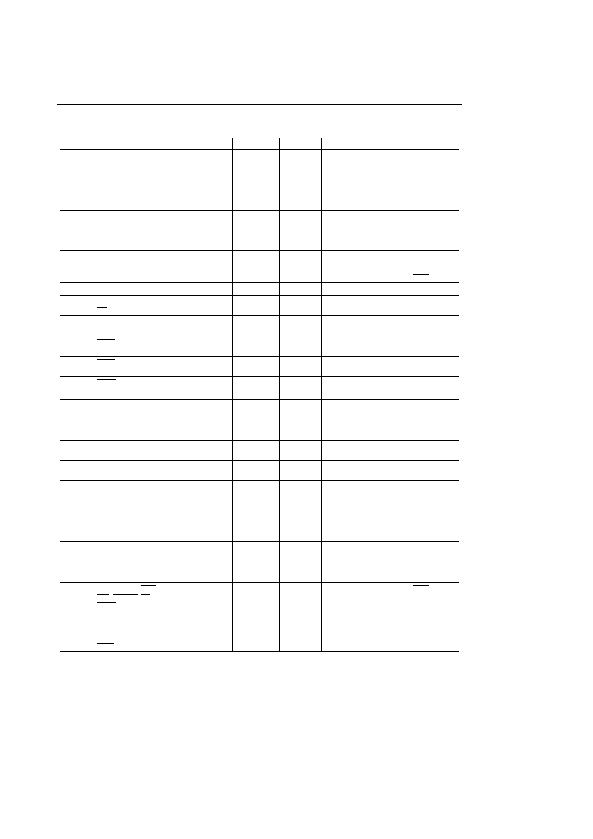
12.1 Instruction Set Index (Continued)
Alphabetical
Assembly Operation Page
Mnemonic
DI Disable interrupts 54
DJNZ,d Decrement B and jump relative B
i
056
EI Enable interrupts 54
EX (SP),ss Exchange the location (SP) with register ss 50
EX AF,A’F’ Exchange the contents of AF and A’F’ 49
EX DE,HL Exchange the contents of DE and HL 49
EXX Exchange the contents of BC, DE and HL with the contents 50
of B’C, D’E’ and H’L’, respectively
HALT Halt (wait for interrupt or reset) 54
IM 0 Set interrupt mode 0 54
IM 1 Set interrupt mode 1 55
IM 2 Set interrupt mode 2 55
IN A,(n) Load Accumulator with input from device (n) 52
IN r,(C) Load register r with input from device (C) 52
INC m
1
Increment data in memory location m
1
42
INC r Increment register r 37
INC rr Increment contents of register pair rr 43
IND Load location (HL) with input from port (C), decrement HL and B 52
INDR Load location (HL) with input from port (C), decrement HL and B; repeat until B
e
054
INI Load location (HL) with input from port (C), increment HL, decrement B 52
INIR Load location (HL) with input from port (C), increment HL, decrement B; 53
repeat until B
e
0
JP cc,nn Jump to location nn, if condition cc is true 55
JP nn Unconditional jump to location nn 55
JP (ss) Unconditional jump to location (ss) 55
JR d Unconditional jump relative to PC
a
d55
JR kk,d Jump relative to PC
a
d, if kk true 55
LD A,I Load Accumulator with register I contents 32
LD A,m
2
Load Accumulator from location m
2
33
LD A,R Load Accumulator with register R contents 32
LD I,A Load register I with Accumulator contents 32
LD m
1
,n Load memory with immediate data n 33
LD m
1
,r Load memory from register r 32
LD m
2
,A Load memory from Accumulator 33
LD (nn),rr Load memory location nn with register pair rr 34
LD r,m
1
Load register r from memory 33
LD r,n Load register with immediate data n 32
LD R,A Load register R from Accumulator 32
LD r
d,rs
Load destination register rdfrom source register r
s
32
LD rr,(nn) Load register pair rr from memory location nn 35
LD rr,nn Load register pair rr with immediate data nn 34
LD SP,ss Load SP from register pair ss 34
LDD Load location (DE) with location (HL), decrement DE, HL and BC 50
LDDR Load location (DE) with location (HL), decrement DE, HL and BC; repeat until BC
e
051
LDI Load location (DE) with location (HL), increment DE and HL, decrement BC 50
LDIR Load location (DE) with location (HL), increment DE and HL, decrement BC; 51
repeat until BC
e
0
NEG Negate Accumulator (2’s complement) 38
NOP No operation 54
29
Page 30

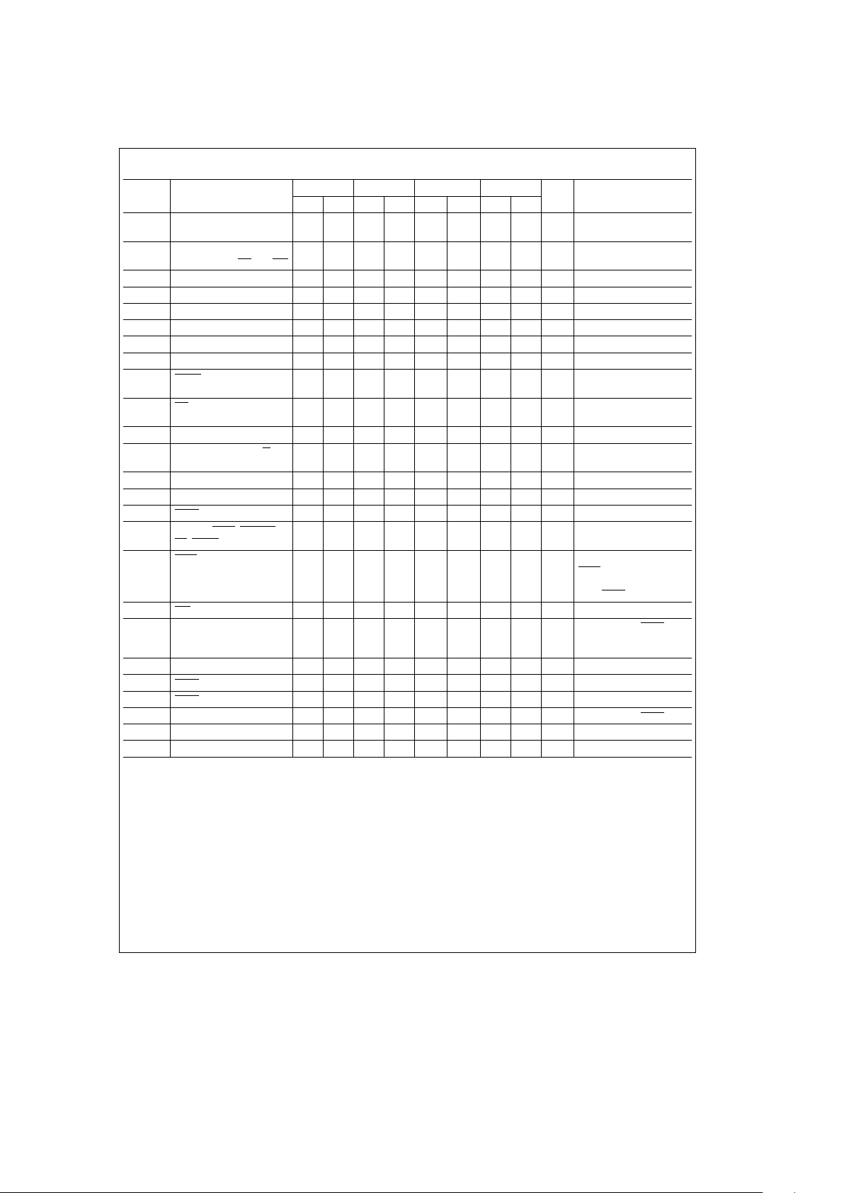
12.1 Instruction Set Index (Continued)
Alphabetical
Assembly Operation Page
Mnemonic
OR m
1
Logical ‘OR’ of memory location contents and accumulator 41
OR n Logical ‘OR’ of immediate data n and Accumulator 39
OR r Logical ‘OR’ of register r and Accumulator 37
OTDR Load output port (C) with location (HL), decrement HL and B; repeat until B
e
054
OTIR Load output port (C) with location (HL), increment HL, decrement B; 53
repeat until B
e
0
OUT (C),r Load output port (C) with register r 52
OUT (n),A Load output port (n) with Accumulator 53
OUTD Load output port (C) with location (HL), decrement HL and B 53
OUTI Load output port (C) with location (HL), increment HL, decrement B 52
POP qq Load register pair qq with top of stack 35
PUSH qq Load top of stack with register pair qq 35
RES b,m
1
Reset bit b of memory location m
1
44
RES b,r Reset bit b of register r 44
RET Unconditional return from subroutine 56
RET cc Return from subroutine, if cc true 56
RETI Unconditional return from interrupt 56
RETN Unconditional return from non-maskable interrupt 57
RL m
1
Rotate memory contents left through carry 47
RL r Rotate register r left through carry 45
RLA Rotate Accumulator left through carry 45
RLC m
1
Rotate memory contents left circular 47
RLC r Rotate register r left circular 45
RLCA Rotate Accumulator left circular 45
RLD Rotate digit left and right between Accumulator and memory (HL) 49
RR m
1
Rotate memory contents right through carry 48
RR r Rotate register r right through carry 46
RRA Rotate Accumulator right through carry 48
RRC m
1
Rotate memory contents right circular 47
RRC r Rotate register r right circular 45
RRCA Rotate Accumulator right circular 46
RRD Rotate digit right and left between Accumulator and memory (HL) 49
RST P Restart to location P 57
SBC A,m
1
Subtract, with carry, memory contents from Accumulator 41
SBC A,n Subtract, with carry, immediate data n from Accumulator 39
SBC A,r Subtract, with carry, register r from Accumulator 36
SBC HL,pp Subtract, with carry, register pair pp from HL 43
SCF Set carry flag 38
SET b,m
1
Set bit b in memory location m1contents 44
SET b,r Set bit b in register r 44
SLA m
1
Shift memory contents left, arithmetic 48
SLA r Shift register r left, arithmetic 46
SRA m
1
Shift memory contents right, arithmetic 48
SRA r Shift register r right, arithmetic 46
SRL m
1
Shift memory contents right, logical 48
SRL r Shift register r right, logical 46
SUB m
1
Subtract memory contents from Accumulator 40
SUB n Subtract immediate data n from Accumulator 39
SUB r Subtract register r from Accumulator 36
XOR m
1
Exclusive ‘OR’ memory contents and Accumulator 42
XOR n Exclusive ‘OR’ immediate data n and Accumulator 39
XOR r Exclusive ‘OR’ register r and Accumulator 37
30
Page 31

12.0 Instruction Set (Continued)
12.2 INSTRUCTION SET MNEMONIC NOTATION
In the following instruction set listing, the notations used are
shown below.
b: Designates one bit in a register or memory location.
Bit address mode uses this indicator.
cc: Designates condition codes used in conditional
Jumps, Calls, and Return instruction; may be:
NZ
e
Non-Zero (Z flage0)
ZeZero (Z flage1)
NCeNon-Carry (C flage0)
C
e
Carry (C flage1)
POeParity Odd or No Overflow (P/Ve0)
PEeParity Even or Overflow (P/Ve1)
PePositive (Se0)
M
e
Negative (Se1)
d: Designates an 8-bit signed complement displace-
ment. Relative or indexed address modes use this
indicator.
kk: Subset of cc condition codes used in conjunction with
conditional relative jumps; may be NZ, Z, NC or C.
m
1
: Designates (HL), (IXad) or (IYad). Register indirect
or indexed address modes use this indicator.
m
2
: Designates (BC), (DE) or (nn). Register indirect or di-
rect address modes use this indicator.
n: Any 8-bit binary number.
nn: Any 16-bit binary number.
p: Designates restart vectors and may be the hex values
0, 8, 10, 18, 20, 28, 30 or 38. Restart instructions
employing the modified page zero addressing mode
use this indicator.
pp: Designates the BC, DE, SP or any 16-bit register used
as a destination operand in 16-bit arithmetic operations employing the register address mode.
qq: Designates BC, DE, HL, A, F, IX, or IY during opera-
tions employing register address mode.
r: Designates A, B, C, D, E, H or L. Register addressing
modes use this indicator.
rr: Designates BC, DE, HL, SP, IX or IY. Register ad-
dressing modes use this indicator.
ss: Designates HL, IX or IY. Register addressing modes
use this indicator.
X
L
: Subscript L indicates the lower-order byte of a 16-bit
register.
X
H
: Subscript H indicates the high-order byte of a 16-bit
register.
( ): parentheses indicate the contents are considered a
pointer address to a memory or I/O location.
12.3 ASSEMBLED OBJECT CODE NOTATION
Register Codes:
r Register rp Register rs Register
000 B 00BC00BC
001 C 01DE01DE
010 D 10HL10HL
011 E 11SP11AF
100 H pp Register qq Register
101 L 00BC00BC
111 A 01DE01DE
10 IX 10 HL
11 SP 11 AF
Conditions Codes:
cc Mnemonic True Flag Condition
000 NZ Z
e
0
001 Z Z
e
1
010 NC C
e
0
011 C C
e
1
100 PO P/V
e
0
101 PE P/V
e
1
110 P S
e
0
111 M S
e
1
kk Mnemonic True Flag Condition
00 NZ Z
e
0
01 Z Z
e
1
10 NC C
e
0
11 C C
e
1
Restart Addresses:
tT
000 X’00
001 X’08
010 X’10
011 X’18
100 X’20
101 X’28
110 X’30
111 X’38
31
Page 32

12.4 8-Bit Loads
REGISTER TO REGISTER
LD r
d,rs
Load register rdwith rs:
r
d
w
r
s
No flags affected
76543210
01 r
d
r
s
Timing: M cycles Ð 1
T states Ð 4
Addressing Mode: Register
LD A, I
Load Accumulator with the contents of the I register.
A
w
I S: Set if negative result
Z: Set if zero result
H: Reset
P/V: Set according to IFF
2
(zero if
interrupt occurs during operation)
N: Reset
C: Not affected
76543210
11101101
01010111
Timing: M cycles Ð 2
T states Ð 9 (4, 5)
Addressing Mode: Register
LD I, A
Load Interrupt vector register (I) with the contents of A.
I
w
A No flags affected
76543210
11101101
01000111
Timing: M cycles Ð 2
T states Ð 9 (4, 5)
Addressing Mode: Register
LD A, R
Load Accumulator with contents of R register.
A
w
R S: Set if negative result
Z: Set if zero result
H: Reset
P/V: Set according to IFF
2
(zero if
interrupt occurs during operation)
N: Reset
C: Not affected
76543210
11101101
01011111
Timing: M cycles Ð 2
T states Ð 9 (4, 5)
Addressing Mode: Register
LD R, A
Load Refresh register (R) with contents of the Accumulator.
R
w
A No flags affected
76543210
11101101
01001111
Timing: M cycles Ð 2
T states Ð 9 (4, 5)
Addressing Mode: Register
LD r, n
Load register r with immediate data n.
r
w
n No flags affected
76543210
00 r 110
n
Timing: M cycles Ð 2
T states Ð 7 (4, 3)
Addressing Mode: Source Ð Immediate
Destination Ð Register
REGISTER TO MEMORY
LD m
1
,r
Load memory from reigster r.
m
1
w
r No flags affected
76543210
01110 r LD(HL), r
Timing: M cycles Ð 2
T states Ð 7 (4,3)
Addressing Mode: Source Ð Register
Destination Ð Register Indirect
76 5 43210
LD (IX
a
d), r(for N
X
e
0)
11NX11101
LD (IY
a
d), r(for N
X
e
1)
01110 r
d
Timing: M cycles Ð 2
T states Ð 19 (4, 4, 3, 5, 3)
Addressing Mode: Source Ð Register
Destination Ð Indexed
32
Page 33

12.4 8-Bit Loads (Continued)
LD m
2
,A
Load memory from the Accumulator.
m
2
w
A No flags affected
76543210
00000010LD(BC), A
00010010LD(DE), A
Timing: M cycles Ð 2
T states Ð 7 (4, 3)
Addressing Mode: Source Ð Register (Implied)
Destination Ð Register Indirect
76543210
00110010LD(nn), A
n (low-order byte)
n (high-order byte)
Timing: M cycles Ð 4
T states Ð 3 (4, 3, 3, 3)
Addressing Mode: Source Ð Register (Implied)
Destination Ð Direct
LD m
1
,n
Load memory with immediate data.
m
1
w
n No flags affected
76543210
00110110 LD(HL), n
n
Timing: M cyclesÐ3
T statesÐ10 (4, 3, 3)
Addressing Mode: SourceÐImmediate
DestinationÐRegister Indirect
76 5 43210
LD (IX
a
d), n(for N
X
e
0)
11NX11101
LD (IY
a
d), n(for N
X
e
1)
00 1 10110
d
n
Timing: M cyclesÐ5
T statesÐ19 (4, 4, 3, 5, 3)
Addressing Mode: SourceÐImmediate
DestinationÐIndexed
MEMORY TO REGISTER
LD r, m
1
Load register r from memory location m1.
rwm
1
No flags affected
76543210
0 1 r 1 1 0 LD R, (HL)
Timing: M cyclesÐ2
T statesÐ7 (4, 3)
Addressing Mode: SourceÐRegister Indirect
DestinationÐRegister
76 5 43210
LD r, (IX
a
d) (for N
X
e
0)
11NX11101
LD r, (IY
a
d) (for N
X
e
1)
01 r 110
d
Timing: M cyclesÐ5
T statesÐ19 (4, 4, 3, 5, 3)
Addressing Mode: SourceÐIndexed
DestinationÐRegister
LD A, m
2
Load the Accumulator from memory location m2.
A
w
m
2
No flags affected
76543210
LD A, (BC)
00001010
00011010 LDA,(DE)
Timing: M cyclesÐ2
T statesÐ7 (4, 3)
Addressing Mode: SourceÐRegister Indirect
DestinationÐRegister (Implied)
76543210
00111010 LDA,(nn)
n (low-order byte)
n (high-order byte)
Timing: M cyclesÐ4
T statesÐ13 (4, 3, 3, 3)
Addressing Mode: SourceÐImmediate Extended
DestinationÐRegister (Implied)
33
Page 34

12.5 16-Bit Loads
REGISTER TO REGISTER
LD rr, nn
Load 16-bit register pair with immediate data.
rr,
w
nn No flags affected
76543210
LD BC, nn
LD DE, nn
00 rp 0001
LD HL, nn
LD SP, nn
n (low-order byte)
n (high-order byte)
Timing: M cyclesÐ3
T statesÐ10 (4, 3, 3)
Addressing Mode: SourceÐImmediate Extended
DestinationÐRegister
76 5 43210
LD IX, nn (for N
X
e
0)
11NX11101
LD IY, nn (for N
X
e
1)
00 1 00001
n (low-order byte)
n (high-order byte)
Timing: M cyclesÐ4
T statesÐ14 (4, 4, 3, 3)
Addressing Mode: SourceÐImmediate Extended
DestinationÐRegister
LD SP, ss
Load the SP from 16-bit register ss.
SP
w
ss No flags affected
76543210
11111001 LDSP,HL
Timing: M cyclesÐ1
T statesÐ6
Addressing Mode: SourceÐRegister
DestinationÐRegister (Implied)
76 5 43210
LD SP, IX (for N
X
e
0)
11NX11101
LD SP, IY (for N
X
e
1)
11 1 11001
Timing: M cyclesÐ2
T statesÐ10 (4, 6)
Addressing Mode: SourceÐRegister
DestinationÐRegister (Implied)
REGISTER TO MEMORY
LD (nn), rr
Load memory location nn with contents of 16-bit register, rr.
(nn)
w
rr
L
No flags affected
(nna1)wrr
H
76543210
LD (nn), HL
(note an alternate
00100010
opcode below)
n (low-order byte)
n (high-order byte)
Timing: M cyclesÐ5
T statesÐ16 (4, 3, 3, 3, 3)
Addressing Mode: SourceÐRegister
DestinationÐDirect
76543210
LD (nn), BC
LD (nn), DE
11101101
LD (nn), HL
LD (nn), SP
01 rp 0011
n (low-order byte)
n (high-order byte)
Timing: M cyclesÐ6
T statesÐ20 (4, 4, 3, 3, 3, 3)
Addressing Mode: SourceÐRegister
DestinationÐDirect
76 5 43210
LD (nn), IX (for N
X
e
0)
11NX11101
LD (nn) IY (for N
X
e
1)
00 1 00010
n (low-order byte)
n (high-order byte)
Timing: M cyclesÐ6
T statesÐ20 (4, 4, 3, 3, 3, 3)
Addressing Mode: SourceÐRegister
DestinationÐDirect
34
Page 35

12.5 16-Bit Loads (Continued)
PUSH qq
Push the contents of register pair qq onto the memory
stack.
(SP–1)
w
qq
H
No flags affected
(SP–2)wqq
L
SPwSPb2
76543210PUSH BC
11 rs 0101
PUSH DE
PUSH HL
PUSH AF
Timing: M cyclesÐ3
T statesÐ11 (5, 3, 3)
Addressing Mode: SourceÐRegister
DestinationÐRegister Indirect
(Stack)
76 5 43210
PUSH IX (for N
X
e
0)
11NX11101
PUSH IY (for N
X
e
1)
11 1 00101
Timing: M cyclesÐ3
T statesÐ15 (4, 5, 3, 3)
Addressing Mode: SourceÐRegister
DestinationÐRegister Indirect
(Stack)
MEMORY TO REGISTER
LD rr, (nn)
Load 16-bit register from memory location nn.
rr
L
w
(nn) No flags affected
rr
H
w
(nna1)
76543210
LD HL, (nn)
00101010
(note an alternate
opcode below)
n (low-order byte)
n (high-order byte)
Timing: M cyclesÐ5
T statesÐ16 (4, 3, 3, 3, 3)
Addressing Mode: SourceÐDirect
DestinationÐRegister
76543210
LD BC, (nn)
LD DE, (nn)
11101101
LD HL, (nn)
LD SP, (nn)
01 rp 0011
n (low-order byte)
n (high-order byte)
Timing: M cyclesÐ6
T statesÐ20 (4, 4, 3, 3, 3, 3)
Addressing Mode: SourceÐDirect
DestinationÐRegister
76 5 43210
LD IX, (nn)(for N
X
e
0)
11NX11101
LD IY, (nn) (for N
X
e
1)
00 1 01010
n (low-order byte)
n (high-order byte)
Timing: M cyclesÐ6
T statesÐ20 (4, 4, 3, 3, 3, 3)
Addressing Mode: SourceÐDirect
DestinationÐRegister
POP qq
Pop the contents of the memory stack to register qq.
qq
L
w
(SP) No flags affected
qq
H
w
(SPa1)
SPwSPa2
76543210POP BC
11 rs 0001
POP DE
POP HL
POP AF
Timing: M cyclesÐ3
T statesÐ10 (4, 3, 3)
Addressing Mode: SourceÐRegister Indirect
(Stack)
DestinationÐRegister
76 5 43210
POP IX (for N
X
e
0)
11NX11101
POP IY (for N
X
e
1)
11 1 00001
Timing: M cyclesÐ4
T statesÐ14 (4, 4, 3, 3)
Addressing Mode: SourceÐRegister Indirect
(Stack)
DestinationÐRegister
35
Page 36

12.6 8-Bit Arithmetic
REGISTER ADDRESSING ARITHMETIC
Hex Hex
C
Value
H
Value Number
C
Op Before
In
Before
In Added
After
DAA
Upper
DAA
Lower To
DAA
Digit Digit Byte
(Bits 7-4) (Bits 3-0)
0 0-9 0 0-9 00 0
0 0-8 0 A-F 06 0
0 0-9 1 0-3 06 0
ADD 0 A-F 0 0-9 60 1
ADC 0 9-F 0 A-F 66 1
INC 0 A-F 1 0-3 66 1
1 0-2 0 0-9 60 1
1 0-2 0 A-F 66 1
1 0-3 1 0-3 66 1
SUB 0 0-9 0 0-9 00 0
SBC 0 0-8 1 6-F FA 0
DEC 1 7-F 0 0-9 A0 1
NEG 1 6-F 1 6-F 9A 1
ADD A, r
Add contents of register r to the
Accumulator.
A
w
Aar S: Set if negative result
Z: Set if zero result
H: Set if carry from bit 3
P/V: Set according to overflow
condition
N: Reset
C: Set if carry from bit 7
76543210
10000 r
Timing: M cyclesÐ1
T statesÐ4
Addressing Mode: SourceÐRegister
DestinationÐImplied
ADC A, r
Add contents of register r, plus the carry flag, to the Accumulator.
A
w
AaraCY S: Set if negative result
Z: Set if zero result
H: Set if carry from bit 3
P/V: Set if result exceeds 2’s com-
plement range
N: Reset
C: Set if carry from bit 7
76543210
10001 r
Timing: M cyclesÐ1
T statesÐ4
Addressing Mode: SourceÐRegister
DestinationÐImplied
SUB r
Subtract the contents of register r from the Accumulator.
A
w
Abr S: Set if result is negative
Z: Set if result is zero
H: Set if borrow from bit 4
P/V: Set if result exceeds 8-bit 2’s
complement range
N: Set
C: Set according to borrow
76543210
10010 r
Timing: M cyclesÐ1
T statesÐ4
Addressing Mode: SourceÐRegister
DestinationÐImplied
SBC A, r
Subtract contents of register r and the carry bit C from the
Accumulator.
A
w
AbrbCY S: Set if result is negative
Z: Set if result is zero
H: Set if borrow from bit 4
P/V: Set if result exceeds 8-bit 2’s
complement range
N: Set
C: Set according to borrow
76543210
10011 r
Timing: M cyclesÐ1
T statesÐ4
Addressing Mode: SourceÐRegister
DestinationÐImplied
AND r
Logically AND the contents of the r register and the Accumulator.
A
w
A ! r S: Set if result is negative
Z: Set if result is zero
H: Set
P/V: Set if result parity is even
N: Reset
C: Reset
36
Page 37

12.6 8-Bit Arithmetic (Continued)
76543210
10100 r
Timing: M cyclesÐ1
T statesÐ4
Addressing Mode: SourceÐRegister
DestinationÐImplied
OR r
Logically OR the contents of the r register and the Accumulator.
A
w
A ¶ r S: Set if result is negative
Z: Set if result is zero
H: Reset
P/V: Set if result parity is even
N: Reset
C: Reset
76543210
10110 r
Timing: M cyclesÐ1
T statesÐ4
Addressing Mode: SourceÐRegister
DestinationÐImplied
XOR r
Logically exclusively OR the contents of the r register with
the Accumulator.
A
w
AZr S: Set if result is negative
Z: Set if result is zero
H: Reset
P/V: Set if result parity is even
N: Reset
C: Reset
76543210
10101 r
Timing: M cyclesÐ1
T statesÐ4
Addressing Mode: SourceÐRegister
DestinationÐImplied
INC r
Increment register r.
r
w
ra1 S: Set if result is negative
Z: Set if result is zero
H: Set if carry from bit 3
P/V: Set only if r was X’7F before
operation
N: Reset
C: N/A
76543210
00 r 100
Timing: M cyclesÐ1
T statesÐ4
Addressing Mode: SourceÐRegister
DestinationÐRegister
CP r
Compare the contents of register r with the Accumulator
and set the flags accordingly.
A
b
r S: Set if result is negative
Z: Set if result is zero
H: Set if borrow from bit 4
P/V: Set if result exceeds 8-bit 2’s
complement range
N: Set
C: Set according to borrow
76543210
10111 r
Timing: M cyclesÐ1
T statesÐ4
Addressing Mode: SourceÐRegister
DestinationÐImplied
DEC r
Decrement the contents of register r.
r
w
rb1 S: Set if result is negative
Z: Set if result is zero
H: Set according to a borrow from
bit 4
P/V: Set only if r was X’80 prior to
operation
N: Set
C: N/A
76543210
00 r 101
Timing: M cyclesÐ1
T statesÐ4
Addressing Mode: SourceÐRegister
DestinationÐRegister
CPL
Complement the Accumulator (1’s complement).
A
w
A S: N/A
Z: N/A
H: Set
P/V: N/A
N: Set
C: N/A
37
Page 38

12.6 8-Bit Arithmetic (Continued)
76543210
00101111
Timing: M cyclesÐ1
T statesÐ4
Addressing Mode: Implied
NEG
Negate the Accumulator (2’s complement).
A
w
0bA S: Set if result is negative
Z: Set if result is zero
H: Set according to borrow from
bit 4
P/V: Set only if Accumulator was
X’80 prior to operation
N: Set
C: Set only if Accumulator was not
X’00 prior to operation
76543210
11101101
01000100
Timing: M cyclesÐ2
T statesÐ8 (4, 4)
Addressing Mode: Implied
CCF
Complement the carry flag.
CY
w
CY S: N/A
Z: N/A
H: Previous carry
P/V: N/A
N: Reset
C: Complement of previous carry
76543210
00111111
Timing: M cyclesÐ1
T statesÐ4
Addressing Mode: Implied
SCF
Set the carry flag.
CY
w
1 S: N/A
Z: N/A
H: Reset
P/V: N/A
N: Reset
C: Set
76543210
00110111
Timing: M cyclesÐ1
T statesÐ4
Addressing Mode: Implied
DAA
Adjust the Accumulator for BCD addition and subtraction
operations. To be executed after BCD data has been operated upon the standard binary ADD, ADC, INC, SUB, SBC,
DEC or NEG instructions (see ‘‘Register Addressing Arithmetic’’ table).
ÐÐÐ S: Set according to bit 7 of result
Z: Set if result is zero
H: Set according to instructions
P/V: Set according to parity of result
N: N/A
C: Set according to instructions
76543210
00100111
Timing: M cyclesÐ1
T statesÐ4
Addressing Mode: Implied
IMMEDIATELY ADDRESSED ARITHMETIC
ADD A, n
Add the immediate data n to the Accumulator.
A
w
Aan S: Set if result is negative
Z: Set if result is zero
H: Set if carry from bit 3
P/V: Set if result exceeds 8-bit 2’s
complement range
N: Reset
C: Set if carry from bit 7
76543210
11000110
n
Timing: M cyclesÐ2
T statesÐ7 (4, 3)
Addressing Mode: SourceÐImmediate
DestinationÐImplied
ADC A, n
Add, with carry, the immediate data n and the Accumulator.
A
w
AanaCY S: Set if result is negative
Z: Set if result is zero
H: Set if carry from bit 3
P/V: Set if result exceeds 8-bit 2’s
complement range
N: Reset
C: Set according to carry from bit
7
38
Page 39

12.6 8-Bit Arithmetic (Continued)
76543210
11001110
n
Timing: M cyclesÐ2
T statesÐ7 (4, 3)
Addressing Mode: SourceÐImmediate
DestinationÐImplied
SUB n
Subtract the immediate data n from the Accumulator.
A
w
Abn S: Set if result is negative
Z: Set if result is zero
H: Set if borrow from bit 4
P/V: Set if result exceeds 8-bit 2’s
complement range
N: Set
C: Set according to borrow
condition
76543210
11010110
n
Timing: M cyclesÐ2
T statesÐ7 (4, 3)
Addressing Mode: SourceÐImmediate
DestinationÐImplied
SBC A, n
Subtract, with carry, the immediate data n from the Accumulator.
A
w
AbnbCY S: Set if result is negative
Z: Set if result is zero
H: Set if borrow from bit 4
P/V: Set if result exceeds 8-bit 2’s
complement range
N: Set
C: Set according to borrow
condition
76543210
11011110
n
Timing: M cyclesÐ2
T statesÐ7 (4, 3)
Addressing Mode: SourceÐImmediate
DestinationÐImplied
AND n
The immediate data n is logically AND’ed to the Accumulator.
A
w
A ! n S: Set if result is negative
Z: Set if result is zero
H: Set
P/V: Set if result parity is even
N: Reset
C: Reset
76543210
11100110
n
Timing: M cyclesÐ2
T statesÐ7 (4, 3)
Addressing Mode: SourceÐImmediate
DestinationÐImplied
OR n
The immediate data n is logically OR’ed to the contents of
the Accumulator.
A
w
A ¶ s S: Set if result is negative
Z: Set if result is zero
H: Reset
P/V: Set if result parity is even
N: Reset
C: Reset
76543210
11110110
n
Timing: M cyclesÐ2
T statesÐ7 (4, 3)
Addressing Mode: SourceÐImmediate
DestinationÐImplied
XOR n
The immediate data n is exclusively OR’ed with the Accumulator.
A
w
AZn S: Set if result is negative
Z: Set if result is zero
H: Reset
P/V: Set if result parity is even
N: Reset
C: Reset
39
Page 40

12.6 8-Bit Arithmetic (Continued)
76543210
11101110
n
Timing: M cyclesÐ2
T statesÐ7 (4, 3)
Addressing Mode: SourceÐImmediate
DestinationÐImplied
CP n
Compare the immediate data n with the contents of the Accumulator via subtraction and return the appropriate flags.
The contents of the Accumulator are not affected.
A
b
n S: Set if result is negative
Z: Set if result is zero
H: Set if borrow from bit 4
P/V: Set if result exceeds 8-bit 2’s
complement range
N: Set
C: Set according to borrow condi-
tion
76543210
11111110
n
Timing: M cyclesÐ2
T statesÐ7 (4, 3)
Addressing Mode: Immediate
MEMORY ADDRESSED ARITHMETIC
ADD A, m1
Add the contents of the memory location m
1
to the Accumu-
lator.
A
w
Aam
1
S: Set if result is negative
Z: Set if result is zero
H: Set if carry from bit 3
P/V: Set if result exceeds 8-bit 2’s
complement range
N: Reset
C: Set according to carry from bit
7
76543210
10000110 ADDA,(HL)
Timing: M cyclesÐ2
T statesÐ7 (4, 3)
Addressing Mode: SourceÐRegister Indirect
DestinationÐImplied
76 5 43210
ADD A, (IX
a
d) (for N
X
e
0)
11NX11101
ADD A, (IY
a
d) (for N
X
e
1)
10 0 00110
d
Timing: M cyclesÐ5
T statesÐ19 (4, 4, 3, 5, 3)
Addressing Mode: SourceÐIndexed
DestinationÐImplied
ADC A, m
1
Add the contents of the memory location m1plus the carry
to the Accumulator.
A
w
Aam
1
a
CY S: Set if result is negative
Z: Set if result is zero
H: Set if carry from bit 3
P/V: Set if result exceeds 8-bit 2’s
complement range
N: Reset
C: Set according to carry from bit
7
76543210
10001110 ADCA,(HL)
Timing: M cyclesÐ2
T statesÐ7 (4, 3)
Addressing Mode: SourceÐRegister Indirect
DestinationÐImplied
76 5 43210
ADC A, (IX
a
d) (for N
X
e
0)
11NX11101
ADC A, (IY
a
d) (for N
X
e
1)
10 0 01110
d
Timing: M cyclesÐ5
T statesÐ19 (4, 4, 3, 5, 3)
Addressing Mode: SourceÐIndexed
DestinationÐImplied
SUB m
1
Subtract the contents of memory location m1from the Accumulator.
A
w
Abm
1
S: Set if result is negative
Z: Set if result is zero
H: Set if borrow from bit 4
P/V: Set if result exceeds 8-bit 2’s
complement range
N: Set
C: Set according to borrow condi-
tion
40
Page 41

12.6 8-Bit Arithmetic (Continued)
76543210
10010110 SUB(HL)
Timing: M cyclesÐ2
T statesÐ7 (4, 3)
Addressing Mode: SourceÐRegister Indirect
DestinationÐImplied
76 5 43210
SUB (IX
a
d) (for N
X
e
0)
11NX11101
SUB (IY
a
d) (for N
X
e
1)
10 0 10110
d
Timing: M cyclesÐ5
T statesÐ19 (4, 4, 3, 5, 3)
Addressing Mode: SourceÐIndexed
DestinationÐImplied
SBC A, m
1
Subtract, with carry, the contents of memory location m
1
from the Accumulator.
AwAbm
1
b
CY S: Set if result is negative
Z: Set if result is zero
H: Set if carry from bit 3
P/V: Set if result exceeds 8-bit 2’s
complement range
N: Set
C: Set according to borrow
condition
76543210
10011110 SBCA,(HL)
Timing: M cyclesÐ2
T statesÐ7 (4, 3)
Addressing Mode: SourceÐRegister Indirect
DestinationÐImplied
76 5 43210
SBC A, (IX
a
d) (for N
X
e
0)
11NX11101
SBC A, (IY
a
d) (for N
X
e
1)
10 0 11110
d
Timing: M cyclesÐ5
T statesÐ19 (4, 4, 3, 5, 3)
Addressing Mode: SourceÐIndexed
DestinationÐImplied
AND m
1
The data in memory location m1is logically AND’ed to the
Accumulator.
A
w
A ! m
1
S: Set if result is negative
Z: Set if result is zero
H: Set
P/V: Set if result parity is even
N: Reset
C: Reset
76543210
10100110 AND(HL)
Timing: M cyclesÐ2
T statesÐ7 (4, 3)
Addressing Mode: SourceÐRegister Indirect
DestinationÐImplied
76 5 43210
AND (IX
a
d) (for N
X
e
0)
11NX11101
AND (IY
a
d) (for N
X
e
1)
10 1 00110
d
Timing: M cyclesÐ5
T statesÐ19 (4, 4, 3, 5, 3)
Addressing Mode: SourceÐIndexed
DestinationÐImplied
OR m
1
The data in memory location m1is logically OR’ed with the
Accumulator.
A
w
A ¶ m
1
S: Set if result is negative
Z: Set if result is zero
H: Reset
P/V: Set if result parity is even
N: Reset
C: Reset
76543210
10110110 OR(HL)
Timing: M cyclesÐ2
T statesÐ7 (4, 3)
Addressing Mode: SourceÐRegister Indexed
DestinationÐImplied
76 5 43210
OR (IX
a
d) (for N
X
e
0)
11NX11101
OR (IY
a
d) (for N
X
e
1)
10 1 10110
d
Timing: M cyclesÐ5
T statesÐ19 (4, 4, 3, 5, 3)
Addressing Mode: SourceÐIndexed
DestinationÐImplied
41
Page 42

12.6 8-Bit Arithmetic (Continued)
XOR m
1
The data in memory location m1is exclusively OR’ed with
the data in the Accumulator.
A
w
AZm
1
S: Set if result is negative
Z: Set if result is zero
H: Reset
P/V: Set if result parity is even
N: Reset
C: Reset
76543210
10101110 XOR(HL)
Timing: M cyclesÐ2
T statesÐ7 (4, 3)
Addressing Mode: SourceÐRegister Indexed
DestinationÐImplied
76 5 43210
XOR (IX
a
d) (for N
X
e
0)
11NX11101
XOR (IY
a
d) (for N
X
e
1)
10 1 01110
d
Timing: M cyclesÐ5
T statesÐ19 (4, 4, 3, 5, 3)
Addressing Mode: SourceÐIndexed
DestinationÐImplied
CP m
1
Compare the data in memory location m1with the data in
the Accumulator via subtraction.
A
b
m
1
S: Set if result is negative
Z: Set if result is zero
H: Set if borrow from bit 4
P/V: Set if result exceeds 8-bit 2’s
complement range
N: Set
C: Set according to borrow
condition
76543210
10111110 CP(HL)
Timing: M cyclesÐ2
T statesÐ7 (4, 3)
Addressing Mode: SourceÐRegister Indirect
DestinationÐImplied
76 5 43210
CP (IX
a
d) (for N
X
e
0)
11NX11101
CP (IY
a
d) (for N
X
e
1)
10 1 11110
d
Timing: M cyclesÐ5
T statesÐ19 (4, 4, 3, 5, 3)
Addressing Mode: SourceÐIndexed
DestinationÐImplied
INC m
1
Increment data in memory location m1.
m
1
w
m
1
a
1 S: Set if result is negative
Z: Set if result is zero
H: Set according to carry from bit
3
P/V: Set if data was X’7F before op-
eration
N: Reset
C: N/A
76543210
00110100 INC(HL)
Timing: M cyclesÐ3
T statesÐ11 (4, 4, 3)
Addressing Mode: SourceÐRegister Indexed
DestinationÐRegister Indexed
76 5 43210
INC (IX
a
d) (for N
X
e
0)
11NX11101
INC (IY
a
d) (for N
X
e
1)
00 1 10100
d
Timing: M cyclesÐ6
T statesÐ23 (4, 4, 3, 5, 4, 3)
Addressing Mode: SourceÐIndexed
DestinationÐIndexed
DEC m
1
Decrement data in memory location m1.
m
1
w
m
1
b
1 S: Set if result is negative
Z: Set if result is zero
H: Set according to borrow from
bit 4
P/V: Set only if m
1
was X’80 before
operation
N: Set
C: N/A
42
Page 43

12.6 8-Bit Arithmetic (Continued)
76543210
0 0 1 1 0 1 0 1 DEC (HL)
Timing: M cycles Ð 3
T states Ð 11 (4, 4, 3)
Addressing Mode: Source Ð Register Indexed
Destination Ð Register Indexed
76 5 43210
DEC (IX
a
d) (for N
X
e
0)
11NX11101
DEC (IY
a
d) (for N
X
e
1)
00 1 10101
d
Timing: M cycles Ð 6
T states Ð 23 (4, 4, 3, 5, 4, 3)
Addressing Mode: Source Ð Indexed
Destination Ð Indexed
12.7 16-Bit Arithmetic
ADD ss, pp
Add the contents of the 16-bit register rp or pp to the contents of the 16-bit register ss.
ss
w
ssarp S: N/A
or Z: N/A
sswssapp H: Set if carry from bit 11
P/V: N/A
N: Reset
C: Set if carry from bit 15
76543210
0 0 rp 1 0 0 1 ADD HL, rp
Timing: M cycles Ð 3
T states Ð 11 (4, 4, 3)
Addressing Mode: Source Ð Register
Destination Ð Register
76 5 43210
ADD IX, pp (for N
X
e
0)
11NX11101
ADD IY, pp (for N
X
e
1)
00 pp 1001
Timing: M cycles Ð 4
T states Ð 15 (4, 4, 4, 3)
Addressing Mode: Source Ð Register
Destination Ð Register
ADC HL, pp
The contents of the 16-bit register pp are added, with the
carry bit, to the HL register.
HL
w
HLappaCY
S: Set if result is negative
Z: Set if result is zero
H: Set according to carry out of bit
11
P/V: Set if result exceeds 16-bit 2’s
complement range
N: Reset
C: Set if carry out of bit 15
76543210
11101101
01 pp 1010
Timing: M cycles Ð 4
T states Ð 15 (4, 4, 4, 3)
Addressing Mode: Source Ð Register
Destination Ð Register
SBC HL, pp
Subtract, with carry, the contents of the 16-bit pp register
from the 16-bit HL register.
HL
w
HLbppbCY
S: Set if result is negative
Z: Set if result is zero
H: Set according to borrow from
bit 12
P/V: Set if result exceeds 16-bit 2’s
complement range
N: Set
C: Set according to borrow condi-
tion
76543210
11101101
01 pp 0010
Timing: M cycles Ð 4
T states Ð 15 (4, 4, 4, 3)
Addressing Mode: Source Ð Register
Destination Ð Register
INC rr
Increment the contents of the 16-bit register rr.
rr
w
rra1 No flags affected
76543210INC BC
00 rp 0011
INC DE
INC HL
INC SP
Timing: M cycles Ð 1
T states Ð 6
Addressing Mode: Register
76 5 43210
INC IX (for N
X
e
0)
11NX11101
INC IY (for N
X
e
1)
00 1 00011
Timing: M cycles Ð 2
T states Ð 10 (4, 6)
Addressing Mode: Register
43
Page 44

12.7 16-Bit Arithmetic (Continued)
DEC rr
Decrement the contents of the 16-bit register rr.
rr
w
rrb1 No flags affected
76543210DEC BC
00 rp 1011
DEC DE
DEC HL
DEC SP
Timing: M cycles Ð 1
T states Ð 6
Addressing Mode: Register
76 5 43210
DEC IX (for N
X
e
0)
11NX11101
DEC IY (for N
X
e
1)
00 1 01011
Timing: M cycles Ð 2
T states Ð 10 (4, 6)
Addressing Mode: Register
12.8 Bit Set, Reset, and Test
REGISTER
SET b, r
Bit b in register r is set.
R
b
w
1 No flags affected
76543210
11001011
11 b r
Timing: M cycles Ð 2
T states Ð 8 (4, 4)
Addressing Mode: Bit/Register
RES b, r
Bit b in register r is reset.
r
b
w
0 No flags affected
76543210
11001011
10 b r
Timing: M cycles Ð 2
T states Ð 8 (4, 4)
Addressing Mode: Bit/Register
BIT b, r
Bit b in register r is tested with the result put in the Z flag.
Z
w
r
b
S: Undefined
Z: Inverse of tested bit
H: Set
P/V: Undefined
N: Reset
C: N/A
76543210
11001011
01 b r
Timing: M cycles Ð 2
T states Ð 8 (4, 4)
Addressing Mode: Bit/Register
MEMORY
SET b, m
1
Bit b in memory location m1is set.
m
1b
w
1 No flags affected
76543210
1 1 0 0 1 0 1 1 SET b, (HL)
11 b 110
Timing: M cycles Ð 4
T states Ð 15 (4, 4, 4, 3)
Addressing Mode: Bit/Register Indirect
76 5 43210
SET b, (IX
a
d) (for N
X
e
0)
11NX11101
SET b, (IY
a
d) (for N
X
e
1)
11 0 01011
d
11 b 110
Timing: M cycles Ð 6
T states Ð 23 (4, 4, 3, 5, 4, 3)
Addressing Mode: Bit/Indexed
RES b, m
1
Bit b in memory location m1is reset.
m
1b
w
0 No flags affected
76543210
1 1 0 0 1 0 1 1 RES b, (HL)
10b110
Timing: M cycles Ð 4
T states Ð 15 (4, 4, 4, 3)
Addressing Mode: Bit/Register Indirect
76 5 43210
RES b, (IX
a
d) (for N
X
e
0)
11NX11101
RES b, (IY
a
d) (for N
X
e
1)
11 0 01011
d
10 b 110
Timing: M cycles Ð 6
T states Ð 23 (4, 4, 3, 5, 4, 3)
Addressing Mode: Bit/Indexed
44
Page 45

12.8 Bit Set, Reset, and Test (Continued)
BIT B, m
1
Bit b in memory location m1is tested via the Z flag.
Zwm
1b
S: Undefined
Z: Inverse of tested bit
H: Set
P/V: Undefined
N: Reset
C: N/A
76543210
1 1 0 0 1 0 1 1 BIT b, (HL)
01 b 110
Timing: M cycles Ð 3
T states Ð 12 (4, 4, 4)
Addressing Mode: Bit/Register Indirect
76 5 43210
BIT b, (IX
a
d) (for N
X
e
0)
11NX11101
BIT b, (IY
a
d) (for N
X
e
1)
11 0 01011
d
01 b 110
Timing: M cycles Ð 5
T states Ð 20 (4, 4, 3, 5, 4)
Addressing Mode: Bit/Indexed
12.9 Rotate and Shift
REGISTER
RLC r
Rotate register r left circular.
TL/C/5171– 57
S: Set if result is negative
Z: Set if result is zero
H: Reset
P/V: Set if result parity is even
N: Reset
C: Set according to bit 7 of r
76543210
11001011RLCr
0 0 0 0 0 r (Note alternate for
A register below)
Timing: M cycles Ð 2
T states Ð 8 (4, 4)
Addressing Mode: Register
76543210
0 0 0 0 0 1 1 1 RLCA
Timing: M cycles Ð 1
T states Ð 4
Addressing Mode: Implied
(Note RLCA does not affect S, Z, or P/V flags.)
RL r
Rotate register r left through carry.
TL/C/5171– 58
S: Set if result is negative
Z: Set if result is zero
H: Reset
P/V: Set if result parity is even
N: Reset
C: Set according to bit 7 of r
76543210
11001011RLr
00010 r (Note alternate for
A register below)
Timing: M cycles Ð 2
T states Ð 8 (4, 4)
Addressing Mode: Register
76543210
00010111 RLA
Timing: M cycles Ð 1
T states Ð 4
Addressing Mode: Implied
(Note RLA does not affect S, Z, or P/V flags.)
RRC r
Rotate register r right circular.
TL/C/5171– 59
S: Set if result is negative
Z: Set if result is zero
H: Reset
P/V: Set if result parity is even
N: Reset
C: Set according to bit 0 of r
45
Page 46

12.9 Rotate and Shift (Continued)
76543210
11001011 RRCr
0 0 0 0 1 r (Note alternate for
A register below)
Timing: M cycles Ð 2
T states Ð 8 (4, 4)
Addressing Mode: Register
76543210
0 0 0 0 1 1 1 1 RRCA
Timing: M cycles Ð 1
T states Ð 4
Addressing Mode: Implied
(Note RRCA does not affect S, Z, or P/V flags.)
RR r
Rotate register r right through carry.
TL/C/5171– 60
S: Set if result is negative
Z: Set if result is zero
H: Reset
P/V: Set if result parity is even
N: Reset
C: Set according to bit 0 of r
76543210
11001001RRr
00011 r (Note alternate for
A register below)
Timing: M cycles Ð 2
T states Ð 8 (4, 4)
Addressing Mode: Register
76543210
00011111 RRA
Timing: M cycles Ð 1
T states Ð 4
Addressing Mode: Implied
(Note RRA does not affect S, Z, or P/V flags.)
SLA r
Shift register r left arithmetric.
TL/C/5171– 61
S: Set if result is negative
Z: Set if result is zero
H: Reset
P/V: Set if result parity is even
N: Reset
C: Set according to bit 7 of r
76543210
11001011
00100 r
Timing: M cycles Ð 2
T states Ð 8 (4, 4)
Addressing Mode: Register
SRA r
Shift register r right arithmetic.
TL/C/5171– 62
S: Set if result is negative
Z: Set if result is zero
H: Reset
P/V: Set if result parity is even
N: Reset
C: Set according to bit 0 of r
76543210
11001011
00101 r
Timing: M cycles Ð 2
T states Ð 8 (4, 4)
Addressing Mode: Register
SRL r
Shift register r right logical.
TL/C/5171– 63
S: Reset
Z: Set if result is zero
H: Reset
P/V: Set if result parity is even
N: Reset
C: Set according to bit 0 of r
76543210
11001011
00111 r
Timing: M cycles Ð 2
T states Ð 8 (4, 4)
Addressing Mode: Register
46
Page 47

12.9 Rotate and Shift (Continued)
MEMORY
RLC m
1
Rotate date in memory location m1left circular.
TL/C/5171– 64
S: Set if result is negative
Z: Set if result is zero
H: Reset
P/V: Set if result parity is even
N: Reset
C: Set according to bit 7 of m
1
76543210
1 1 0 0 1 0 1 1 RLC (HL)
00000110
Timing: M cycles Ð 4
T states Ð 15 (4, 4, 4, 3)
Addressing Mode: Register indirect
76 5 43210
RLC (IX
a
d) (for N
X
e
0)
11NX11101
RLC (IY
a
d) (for N
X
e
1)
11 0 01011
d
00 0 00110
Timing: M cycles Ð 6
T states Ð 23 (4, 4, 3, 5, 4, 3)
Addressing Mode: Indexed
RL m
1
Rotate the data in memory location m1left though carry.
TL/C/5171– 65
S: Set if result is negative
Z: Set if result is zero
H: Reset
P/V: Set if result parity is even
N: Reset
C: Set according to bit 7 of m
1
76543210
1 1 0 0 1 0 1 1 RL (HL)
00010110
Timing: M cycles Ð 4
T states Ð 15 (4, 4, 4, 3)
Addressing Mode: Register Indirect
76 5 43210
RL (IX
a
d) (for N
X
e
0)
11NX11101
RL (IY
a
d) (for NXe1)
11 0 01011
d
00 0 10110
Timing: M cycles Ð 6
T states Ð 23 (4, 4, 3, 5, 4, 3)
Addressing Mode: Indexed
RRC m
1
Rotate the data in memory location m1right circular.
TL/C/5171– 66
S: Set if result is negative
Z: Set if result is zero
H: Reset
P/V: Set if result parity is even
N: Reset
C: Set according to bit 0 of m
1
76543210
1 1 0 0 1 0 1 1 RRC (HL)
00001110
Timing: M cycles Ð 4
T states Ð 15 (4, 4, 4, 3)
Addressing Mode: Register Indirect
76 5 43210
RRC (IX
a
d) (for N
X
e
0)
11NX11101
RRC (IY
a
d) (for N
X
e
1)
11 0 01011
d
00 0 01110
Timing: M cycles Ð 6
T states Ð 23 (4, 4, 3, 5, 4, 3)
Addressing Mode: Indexed
47
Page 48

12.9 Rotate and Shift (Continued)
RR m
1
Rotate the data in memory location m1right through the
carry.
TL/C/5171– 67
S: Set if result is negative
Z: Set if result is zero
H: Reset
P/V: Set if result parity is even
N: Reset
C: Set according to bit 0 of m
1
76543210
1 1 0 0 1 0 1 1 RR (HL)
00011110
Timing: M cycles Ð 4
T states Ð 15 (4, 4, 4, 3)
Addressing Mode: Register Indirect
76 5 43210
RR (IX
a
d) (for N
X
e
0)
11NX11101
RR (IY
a
d) (for N
X
e
1)
11 0 01011
d
00 0 11110
Timing: M cycles Ð 6
T states Ð 23 (4, 4, 3, 5, 4, 3)
Addressing Mode: Indexed
SLA m
1
Shift the data in memory location m1left arithmetic.
TL/C/5171– 68
S: Set if result is negative
Z: Set if result is zero
H: Reset
P/V: Set if result parity is even
N: Reset
C: Set according to bit 7 of m
1
76543210
1 1 0 0 1 0 1 1 SLA (HL)
00100110
Timing: M cycles Ð 4
T states Ð 15 (4, 4, 4, 3)
Addressing Mode: Register Indirect
76 5 43210
SLA (IX
a
d) (for N
X
e
0)
11NX11101
SLA (IY
a
d) (for N
X
e
1)
11 0 01011
d
00 1 00110
Timing: M cycles Ð 6
T states Ð 23 (4, 4, 3, 5, 4, 3)
Addressing Mode: Indexed
SRA m
1
Shift the data in memory location m1right arithmetic.
TL/C/5171– 69
S: Set if result is negative
Z: Set if result is zero
H: Reset
P/V: Set if result parity is even
N: Reset
C: Set according to bit 0 of m
1
76543210
1 1 0 0 1 0 1 1 SRA (HL)
00101110
Timing: M cycles Ð 4
T states Ð 15 (4, 4, 4, 3)
Addressing Mode: Register Indirect
76 5 43210
SRA (IX
a
d) (for N
X
e
0)
11NX11101
SRA (IY
a
d) (for N
X
e
1)
11 0 01011
d
00 1 01110
Timing: M cycles Ð 6
T states Ð 23 (4, 4, 3, 5, 4, 3)
Addressing Mode: Indexed
SRL m
1
Shift right logical the data in memory location m1.
TL/C/5171– 70
S: Reset
Z: Set if result is zero
H: Reset
P/V: Set if result parity is even
N: Reset
C: Set according to bit 0 of m
1
48
Page 49

12.9 Rotate and Shift (Continued)
76543210
1 1 0 0 1 0 1 1 SRL (HL)
00111110
Timing: M cycles Ð 4
T states Ð 15 (4, 4, 4, 3)
Addressing Mode: Register Indirect
76 5 43210
SRL (IX
a
d) (for N
X
e
0)
11NX11101
SRL (IY
a
d) (for N
X
e
1)
11 0 01011
d
00 1 11110
Timing: M cycles Ð 6
T states Ð 23 (4, 4, 3, 5, 4, 3)
Addressing Mode: Indexed
REGISTER/MEMORY
RLD
Rotate digit left and right between the Accumulator and
memory (HL).
TL/C/5171– 71
S: Set if result is negative
Z: Set if result is zero
H: Reset
P/V: Set if result parity is even
N: Reset
C: N/A
76543210
11101101
01101111
Timing: M cycles Ð 5
T states Ð 18 (4, 4, 3, 4, 3)
Addressing Mode: Implied/Register Indirect
RRD
Rotate digit right and left between the Accumulator and
memory (HL).
TL/C/5171– 72
S: Set if result is negative
Z: Set if result is zero
H: Reset
P/V: Set if result parity is even
N: Reset
C: N/A
76543210
11101101
01100111
Timing: M cycles Ð 5
T states Ð 18 (4, 4, 3, 4, 3)
Addressing Mode: Implied/Register Indirect
12.10 Exchanges
REGISTER/REGISTER
EX DE, HL
Exchange the contents of the 16-bit register pairs DE and
HL.
DE
Ý
HL No flags affected
76543210
11101011
Timing: M cycles Ð 1
T states Ð 4
Addressing Mode: Register
EX AF, A’F’
The contents of the Accumulator and flag register are exchanged with their corresponding alternate registers, that is
A and F are exchanged with A’ and F’.
A
Ý
A’ No flags affected
F
Ý
F’
76543210
00001000
Timing: M cycles Ð 1
T states Ð 4
Addressing Mode: Register
49
Page 50

12.10 Exchanges (Continued)
EXX
Exchange the contents of the BC, DE, and HL registers with
their corresponding alternate register.
BC
Ý
B’C’ No flags affected
DE
Ý
D’E’
HL
Ý
H’L’
76543210
11011001
Timing: M cycles Ð 1
T states Ð 4
Addressing Mode: Implied
REGISTER/MEMORY
EX (SP), ss
Exchange the two bytes at the top of the external memory
stack with the 16-bit register ss.
(SP)
Ý
SS
L
No flags affected
(SPa1)
Ý
SS
H
76543210
1 1 1 0 0 0 1 1 EX (SP), HL
Timing: M cycles Ð 5
T states Ð 19 (4, 3, 4, 3, 5)
Addressing Mode: Register/Register Indirect
76 5 43210
EX (SP), IX (for N
X
e
0)
11NX11101
EX (SP),IY (for N
X
e
1)
11 1 00011
Timing: M cycles Ð 6
T states Ð 23 (4, 4, 3, 4, 3, 5)
Addressing Mode: Register/Register Indirect
12.11 Memory Block Moves and
Searches
SINGLE OPERATIONS
LDI
Move data from memory location (HL) to memory location
(DE), increment memory pointers, and decrement byte
counter BC.
(DE)
w
(HL) S: N/A
DEwDEa1 Z: N/A
HLwHLa1 H: Reset
BCwBCb1 P/V: Set if BCb1i0, other-
wise reset
N: Reset
C: N/A
76543210
11101101
10100000
Timing: M cycles Ð 4
T states Ð 16 (4, 4, 3, 5)
Addressing Mode: Register Indirect
LDD
Move data from memory location (HL) to memory location
(DE), and decrement memory pointer and byte counter BC.
(DE)
w
(HL) S: N/A
DEwDEb1 Z: N/A
HLwHLb1 H: Reset
BCwBCb1 P/V: Set if BCb1i0, other-
wise reset
N: Reset
C: N/A
76543210
11101101
10101000
Timing: M cycles Ð 4
T states Ð 16 (4, 4, 3, 5)
Addressing Mode: Register Indirect
CPI
Compare data in memory location (HL) to the Accumulator,
increment the memory pointer, and decrement the byte
counter. The Z flag is set if the comparison is equal.
A
b
(HL) S: Set if result of comparison sub-
tract is negative
HL
w
HLa1
BC
w
BCb1
Z: Set if result of comparison is
Z
w
1
zero
if A
e
(HL)
H: Set according to borrow from
bit 4
P/V: Set if BC
b
1i0, otherwise
reset
N: Set
C: N/A
76543210
11101101
10100001
Timing: M cycles Ð 4
T states Ð 16 (4, 4, 3, 5)
Addressing Mode: Register Indirect
CPD
Compare data in memory location (HL) to the Accumulator,
and decrement the memory pointer and byte counter. The Z
flag is set if the comparison is equal.
A
b
(HL) S: Set if result is negative
HLwHLb1 Z: Set if result of comparison is
zero
BC
w
BCb1
H: Set according to borrow from
Zw1
bit 4
if Ae(HL)
P/V: Set if BC
b
1i0, otherwise
reset
N: Set
C: N/A
50
Page 51

12.11 Memory Block Moves and Searches (Continued)
76543210
11101101
10101001
Timing: M cycles Ð 4
T states Ð 16 (4, 4, 3, 5)
Addressing Mode: Register Indirect
REPEAT OPERATIONS
LDIR
Move data from memory location (HL) to memory location
(DE), increment memory pointers, decrement byte counter
BC, and repeat until BC
e
0.
(DE)w(HL) S: N/A
DEwDEa1 Z: N/A
HL
w
HLa1 H: Reset
BCwBCb1 P/V: Reset
Repeat until N: Reset
BCe0 C: N/A
76543210
11101101
10110000
Timing: For BCi0 M cycles Ð 5
T states Ð 21 (4, 4, 3, 5, 5)
For BC
e
0 M cycles Ð 4
T states Ð 16 (4, 4, 3, 5)
Addressing Mode: Register Indirect
(Note that each repeat is accomplished by a decrement of
the BC, so that refresh, etc. continues for each cycle.)
LDDR
Move data from memory location (HL) to memory location
(DE), decrement memory pointers and byte counter BC, and
repeat until BC
e
0.
(DE)w(HL) S: N/A
DE
w
DEb1 Z: N/A
HLwHLb1 H: Reset
BCwBCb1 P/V: Reset
Repeat until N: Reset
BC
e
0 C: N/A
76543210
11101101
10111000
Timing: For BCi0 M cycles Ð 5
T states Ð 21 (4, 4, 3, 5, 5)
For BCe0 M cycles Ð 4
T states Ð 16 (4, 4, 3, 5)
Addressing Mode: Register Indirect
(Note that each repeat is accomplished by a decrement of
the BC, so that refresh, etc. continues for each cycle.)
CPIR
Compare data in memory location (HL) to the Accumulator,
increment the memory, decrement the byte counter BC, and
repeat until BC
e
0 or (HL) equals A.
Ab(HL) S: Set if sign of subtraction per-
formed for comparison is nega-
HLwHLa1
tive
BCwBCb1
Z: Set if A
e
(HL), otherwise reset
Repeat until BC
e
0
H: Set according to borrow from
or A
e
(HL)
bit 4
P/V: Set if BC
b
1i0, otherwise
reset
N: Set
C: N/A
76543210
11101101
10110001
Timing: For BCi0 M cycles Ð 5
T states Ð 21 (4, 4, 3, 5, 5)
For BC
e
0 M cycles Ð 4
T states Ð 16 (4, 4, 3, 5)
Addressing Mode: Register Indirect
(Note that each repeat is accomplished by a decrement of
the PC, so that refresh, etc. continues for each cycle.)
CPDR
Compare data in memory location (HL) to the contents of
the Accumulator, decrement the memory pointer and byte
counter BC, and repeat until BC
e
0, or until (HL) equals
the Accumulator.
A
b
(HL) S: Set if sign of subtraction per-
formed for comparison is nega-
HL
w
HLb1
tive
BCwBCb1
Z: Set according to equality of A
Repeat until BCe0
and (HL), set if true
or Ae(HL)
H: Set according to borrow from
bit 4
P/V: Set if BC
b
1i0, otherwise
reset
N: Set
C: N/A
76543210
11101101
10111001
Timing: For BCi0 M cycles Ð 5
T states Ð 21 (4, 4, 3, 5, 5)
For BCe0 M cycles Ð 4
T states Ð 16 (4, 4, 3, 5)
Addressing Mode: Register Indirect
(Note that each repeat is accomplished by a decrement of
the BC, so that refresh, etc. continues for each cycle.)
51
Page 52

12.12 Input/Output
IN A, (n)
Input data to the Accumulator from the I/O device at address N.
A
w
(n) No flags affected
76543210
11011011
n
Timing: M cycles Ð 3
T states Ð 11 (4, 3, 4)
Addressing Mode: Source Ð Direct
Destination Ð Register
IN r, (C)
Input data to register r from the I/O device addressed by the
contents of register C. If r
e
110 only flags are affected.
r
w
(C) S: Set if result is negative
Z: Set if result is zero
H: Reset
P/V: Set if result parity is even
N: Reset
C: N/A
76543210
11101101
01 r 000
Timing: M cycles Ð 3
T states Ð 12 (4, 4, 4)
Addressing Mode: Source Ð Register Indirect
Destination Ð Register
OUT (C), r
Output register r to the I/O device addressed by the contents of register C.
(C)
w
r No flags affected
76543210
11101101
01 r 001
Timing: M cycles Ð 3
T states Ð 12 (4, 4, 4)
Addressing Mode: Source Ð Register
Destination Ð Register Indirect
INI
Input data from the I/O device addressed by the contents of
register C to the memory location pointed to by the contents
of the HL register. The HL pointer is incremented and the
byte counter B is decremented.
(HL)
w
(C) S: Undefined
BwBb1 Z: Set if Bb1e0, otherwise reset
HLwHLa1 H: Undefined
P/V: Undefined
N: Set
C: N/A
76543210
11101101
10100010
Timing: M cycles Ð 4
T states Ð 16 (4, 5, 3, 4)
Addressing Mode: Implied/Source Ð Register In-
direct
Destination Ð Register Indirect
OUTI
Output data from memory location (HL) to the I/O device at
port address (C), increment the memory pointer, and decrement the byte counter B.
(C)
w
(HL) S: Undefined
BwBb1 Z: Set if Bb1e0, otherwise reset
HL
w
HLa1 H: Undefined
P/V: Undefined
N: Set
C: N/A
76543210
11101101
10100011
Timing: M cycles Ð 4
T states Ð 16 (4, 5, 3, 4)
Addressing Mode: Implied/Source Ð Register In-
direct
Destination Ð Register Indirect
IND
Input data from I/O device at port address (C) to memory
location (HL), and decrement HL memory pointer and byte
counter B.
(HL)
w
(C) S: Undefined
HL
w
HLb1 Z: Set if Bb1e0, otherwise reset
BwBb1 H: Undefined
P/V: Undefined
N: Set
C: N/A
76543210
11101101
10101010
Timing: M cycles Ð 4
T states Ð 16 (4, 5, 3, 4)
Addressing Mode: Implied/Source Ð Register In-
direct
Destination Ð Register Indirect
52
Page 53

12.12 Input/Output (Continued)
OUT (n), A
Output the Accumulator to the I/O device at address n.
(n)
w
A No flags affected
76543210
11010011
n
Timing: M cycles Ð 3
T states Ð 11 (4, 3, 4)
Addressing Mode: Source Ð Register
Destination Ð Direct
OUTD
Data is output from memory location (HL) to the I/O device
at port address (C), and the HL memory pointer and byte
counter B are decremented.
(C)
w
(HL) S: Undefined
BwBb1 Z: Set if Bb1e0, otherwise reset
HLwHLb1 H: Undefined
P/V: Undefined
N: Set
C: N/A
76543210
11101101
10101011
Timing: M cycles Ð 4
T states Ð 16 (4, 5, 3, 4)
Addressing Mode: Implied/Source Ð Register In-
direct
Destination Ð Register Indirect
INIR
Data is input from the I/O device at port address (C) to
memory location (HL), the HL memory pointer is incremented, and the byte counter B is decremented. The cycle is
repeated until B
e
0.
(Note that B is tested for zero after it is decremented. By
loading B initially with zero, 256 data transfers will take
place.)
(HL)
w
(C) S: Undefined
HLwHLa1 Z: Set
BwBb1 H: Undefined
Repeat until Be0 P/V: Undefined
N: Set
C: N/A
76543210
11101101
10110010
Timing: For Bi0 M cycles Ð 5
T states Ð 21 (4, 5, 3, 4, 5)
For B
e
0 M cycles Ð 4
T states Ð 16 (4, 5, 3, 4)
Addressing Mode: Implied/Source Ð Register In-
direct
Destination Ð Register Indirect
(Note that at the end of each data transfer cycle, interrupts
may be recognized and two refresh cycles will be performed.)
OTIR
Data is output to the I/O device at port address (C) from
memory location (HL), the HL memory pointer is incremented, and the byte counter B is decremented. The cycles are
repeated until B
e
0.
(Note that B is tested for zero after it is decremented. By
loading B initially with zero, 256 data transfers will take
place.)
(C)
w
(HL) S: Undefined
HLwHLa1 H: Undefined
B
w
Bb1 Z: Set
Repeat until Be0 P/V: Undefined
N: Set
C: N/A
76543210
11101101
10110011
Timing: For Bi0 M cycles Ð 5
T states Ð 21 (4, 5, 3, 4, 5)
For B
e
0 M cycles Ð 4
T states Ð 16 (4, 5, 3, 4)
Addressing Mode: Implied/Source Ð Register In-
direct
Destination Ð Register Indirect
(Note that at the end of each data transfer cycle, interrupts
may be recognized and two refresh cycles will be performed.)
53
Page 54

12.12 Input/Output (Continued)
INDR
Data is input from the I/O device at address (C) to memory
location (HL), then the HL memory pointer is byte counter B
are decremented. The cycle is repeated until B
e
0.
(Note that B is tested for zero after it is decremented. By
loading B initially with zero, 256 data transfers will take
place.)
(HL)
w
(C) S: Undefined
HLwHLb1 Z: Set
BwBb1 H: Undefined
Repeat until Be0 P/V: Undefined
N: Set
C: N/A
76543210
11101101
10110010
Timing: For Bi0 M cycles Ð 5
T states Ð 21 (4, 5, 3, 4, 5)
For Be0 M cycles Ð 4
T states Ð 16 (4, 5, 3, 4)
Addressing Mode: Implied/Source Ð Register In-
direct
Destination Ð Register Indirect
(Note that after each data transfer cycle, interrupts may be
recognized and two refresh cycles are performed.)
OTDR
Data is output from memory location (HL) to the I/O device
at port address (C), then the HL memory pointer and byte
counter B are decremented. The cycle is repeated until B
e
0.
(Note that B is tested for zero after it is decremented. By
loading B initially with zero, 256 data transfers will take
place.)
(C)
w
(HL) S: Undefined
HLwHLb1 Z: Set
BwBb1 H: Undefined
Repeat until B
e
0 P/V: Undefined
N: Set
C: N/A
76543210
11101101
10111011
Timing: For Bi0 M cycles Ð 5
T states Ð 21 (4, 5, 3, 4, 5)
For B
e
0 M cycles Ð 4
T states Ð 16 (4, 5, 3, 4)
Addressing Mode: Implied/Source Ð Register In-
direct
Destination Ð Register Indirect
(Note that after each data transfer cycle the NSC800 will
accept interrupts and perform two refresh cycles.)
12.13 CPU Control
NOP
The CPU performs no operation.
Ð Ð Ð No flags affected
76543210
00000000
Timing: M cycles Ð 1
T states Ð 4
Addressing Mode: N/A
HALT
The CPU halts execution of the program. Dummy op-code
fetches are performed from the next memory location to
keep the refresh circuits active until the CPU is interrupted
or reset from the halted state.
Ð Ð Ð No flags affected
76543210
01110110
Timing: M cycles Ð 1
T states Ð 4
Addressing Mode: N/A
DI
Disable system level interrupts.
IFF
1
w
0 No flags affected
IFF
2
w
0
76543210
11110011
Timing: M cycles Ð 1
T states Ð 4
Addressing Mode: N/A
EI
The system level interrupts are enabled. During execution of
this instruction, and the next one, the maskable interrupts
will be disabled.
IFF
1
w
1 No flags affected
IFF
2
w
1
76543210
11111011
Timing: M cycles Ð 1
T states Ð 4
Addressing Mode: N/A
IM 0
The CPU is placed in interrupt mode 0.
Ð Ð Ð No flags affected
76543210
11101101
01000110
Timing: M cycles Ð 2
T states Ð 8 (4, 4)
Addressing Mode: N/A
54
Page 55

12.13 CPU Control (Continued)
IM 1
The CPU is placed in interrupt mode 1.
Ð Ð Ð No flags affected
76543210
11101101
01010110
Timing: M cycles Ð 2
T states Ð 8 (4, 4)
Addressing Mode: N/A
IM 2
The CPU is placed in interrupt mode 2.
Ð Ð Ð No flags affected
76543210
11101101
01011110
Timing: M cycles Ð 2
T states Ð 8 (4, 4)
Addressing Mode: N/A
12.14 Program Control
JUMPS
JP nn
Unconditional jump to program location nn.
PC
w
nn No flags affected
76543210
11000011
n (low-order byte)
n (high-order byte)
Timing: M cycles Ð 3
T states Ð 10 (4, 3, 3)
Addressing Mode: Direct
JP (ss)
Unconditional jump to program location pointed to by register ss.
PC
w
ss No flags affected
76543210
11101001 JP(HL)
Timing: M cycles Ð 1
T states Ð 4
Addressing Mode: Register Indirect
76 5 43210
JP (IX) (for N
X
e
0)
11NX11101
JP (IY) (for N
X
e
1)
11 1 01001
Timing: M cycles Ð 2
T states Ð 8 (4, 4)
Addressing Mode: Register Indirect
JP cc, nn
Conditionally jump to program location nn based on testable
flag states.
If cc true, No flags affected
PC
w
nn,
otherwise continue
765 4 3210
11 cc 010
n (low-order byte)
n (high-order byte)
Timing: M cycles Ð 3
T states Ð 10 (4, 3, 3)
Addressing Mode: Direct
JR d
Unconditional jump to program location calculated with respect to the program counter and the displacement d.
PC
w
PCad No flags affected
76543210
00011000
db2
Timing: M cycles Ð 3
T states Ð 12 (4, 3, 5)
Addressing Mode: PC Relative
JR kk, d
Conditionally jump to program location calculated with respect to the program counter and the displacement d,
based on limited testable flag states.
If kk true, No flags affected
PC
w
PCad,
otherwise continue
76543210
001 kk 000
db2
Timing: if kk met M cycles Ð 3
(true) T states Ð 12 (4, 3, 5)
if kk not met M cycles Ð 2
(not true) T states Ð 7 (4, 3)
Addressing Mode: PC Relative
55
Page 56

12.14 Program Control (Continued)
DJNZ d
Decrement the B register and conditionally jump to program
location calculated with respect to the program counter and
the displacement d, based on the contents of the B register.
B
w
Bb1 No flags affected
If Be0 continue,
else PCwPCad
76543210
00010000
db2
Timing: If Bi0 M cycles Ð 3
T states Ð 13 (5, 3, 5)
If B
e
0 M cycles Ð 2
T states Ð 8 (5, 3)
Addressing Mode: PC Relative
CALLS
CALL nn
Unconditional call to subroutine at location nn.
(SP
b
1)wPC
H
No flags affected
(SPb2)wPC
L
SPwSPb2
PC
w
nn
76543210
11001101
n (low-order byte)
n (high-order byte)
Timing: M Cycles Ð 5
T states Ð 17 (4, 3, 4, 3, 3)
Addressing Mode: Direct
CALL cc, nn
Conditional call to subroutine at location nn based on testable flag stages.
If cc true, No flags affected
(SP
b
1)wPC
H
(SPb2)wPC
L
SPwSPb2
PC
w
nn,
else continue
765 4 3210
11 cc 100
n (low-order byte)
n (high-order byte)
Timing: If cc true M cycles Ð 5
T states 17 (4, 3, 4, 3, 3)
If cc not true M cycles Ð 3
T states Ð 10 (4, 3, 3)
Addressing Mode: Direct
RETURNS
RET
Unconditional return from subroutine or other return to program location pointed to by the top of the stack.
PC
L
w
(SP) No flags affected
PC
H
w
(SPa1)
SPwSPa2
76543210
11001001
Timing: M cycles Ð 3
T states Ð 10 (4, 3, 3)
Addressing Mode: Register Indirect
RET cc
Conditional return from subroutine or other return to program location pointed to by the top of the stack.
If cc true, No flags affected
PC
L
w
(SP)
PC
H
w
(SPa1)
SPwSPa2,
else continue
76543210
11 cc 000
Timing: If cc true M cycles Ð 3
T states Ð 11 (5, 3, 3)
If cc not true M cycles Ð 1
T states Ð 5
Addressing Mode: Register Indirect
RETI
Unconditional return from interrupt handling subroutine.
Functionally identical to RET instruction. Unique opcode allows monitoring by external hardware.
PC
L
w
(SP) No flags affected
PC
H
w
(SPa1)
SPwSPa2
76543210
11101101
01001101
Timing: M cycles Ð 4
T states Ð 14 (4, 4, 3, 3)
Addressing Mode: Register Indirect
56
Page 57

12.14 Program Control (Continued)
RETN
Unconditional return from non-maskable interrupt handling
subroutine. Functionally similar to RET instruction, except
interrupt enable state is restored to that prior to non-maskable interrupt.
PC
L
w
(SP) No flags affected
PC
H
w
(SPa1)
SPwSPa2
IFF
1
w
IFF
2
76543210
11101101
01000101
Timing: M cycles Ð 4
T states Ð 14 (4, 4, 3, 3)
Addressing Mode: Register Indirect
RESTARTS
RST P
The present contents of the PC are pushed onto the memory stack and the PC is loaded with dedicated program locations as determined by the specific restart executed.
(SP
b
1)wPC
H
No flags affected
(SP
b
2)wPC
L
SPwSPb2
PC
H
w
0
PC
L
w
P
76543210
11t111
Timing: M cycles Ð 3
T states Ð 11 (5, 3, 3)
Addressing Mode: Modified Page Zero
p 00H 08H 10H 18H 20H 28H 30H 38H
t 000 001 010 011 100 101 110 111
57
Page 58

12.15 Instruction Set: Alphabetical Order
ADC A, (HL) 8E
ADC A, (IX
a
d) DD 8Ed
ADC A, (IY
a
d) FD 8Ed
ADC A, A 8F
ADC A, B 88
ADC A, C 89
ADC A, D 8A
ADC A, E 8B
ADC A, H 8C
ADC A, L 8D
ADC A, n CE n
ADC HL, BC ED 4A
ADC HL, DE ED 5A
ADC HL, HL ED 6A
ADC HL, SP ED 7A
ADD A, (HL) 86
ADD A, (IX
a
d) DD 86d
ADD A, (IY
a
d) FD 86d
ADD A, A 87
ADD A, B 80
ADD A, C 81
ADD A, D 82
ADD A, E 83
ADD A, H 84
ADD A, L 85
ADD A, n C6 n
ADD HL, BC 09
ADD HL, DE 19
ADD HL, HL 29
ADD HL, SP 39
ADD IX, BC DD 09
ADD IX, DE DD 19
ADD IX, IX DD 29
ADD IX, SP DD 39
ADD IY, BC FD 09
ADD IY, DE FD 19
ADD IY, IY FD 29
ADD IY, SP FD 39
AND (HL) A6
AND (IX
a
d) DD A6d
AND (IY
a
d) FD A6d
AND A A7
AND B A0
AND C A1
AND D A2
AND E A3
AND H A4
AND L A5
AND n E6 n
BIT 0, (HL) CB 46
BIT 0, (IX
a
d) DD CBd46
BIT 0, (IY
a
d) FD CBd46
BIT 0, A CB 47
BIT 0, B CB 40
BIT 0, C CB 41
BIT 0, D CB 42
BIT 0, E CB 43
BIT 0, H CB 44
BIT 0, L CB 45
BIT 1, (HL) CB 4E
BIT 1, (IX
a
d) DD CBd4E
BIT 1, (IY
a
d) FD CBd4E
BIT 1, A CB 4F
BIT 1, B CB 48
BIT 1, C CB 49
BIT 1, D CB 4A
BIT 1, E CB 4B
BIT 1, H CB 4C
BIT 1, L CB 4D
BIT 2, (HL) CB 56
BIT 2, (IX
a
d) DD CBd56
BIT 2, (IY
a
d) FD CBd56
BIT 2, A CB 57
BIT 2, B CB 50
BIT 2, C CB 51
BIT 2, D CB 52
BIT 2, E CB 53
BIT 2, H CB 54
BIT 2, L CB 55
BIT 3, (HL) CB 5E
BIT 3, (IX
a
d) DD CBd5E
BIT 3, (IY
a
d) FD CBd5E
BIT 3, A CB 5F
BIT 3, B CB 58
BIT 3, C CB 59
BIT 3, D CB 5A
BIT 3, E CB 5B
BIT 3, H CB 5C
BIT 3, L CB 5D
BIT 4, (HL) CB 66
BIT 4, (IX
a
d) DD CBd66
BIT 4, (IY
a
d) FD CBd66
BIT 4, A CB 67
BIT 4, B CB 60
BIT 4, C CB 61
BIT 4, D CB 62
BIT 4, E CB 63
BIT 4, H CB 64
BIT 4, L CB 65
BIT 5, (HL) CB 6E
BIT 5, (IX
a
d) DD CBd6E
BIT 5, (IY
a
d) FD CBd6E
BIT 5, A CB 6F
BIT 5, B CB 68
BIT 5, C CB 69
BIT 5, D CB 6A
(nn)eaddress of memory location designed displacement
nn
e
Data (16 bit) d2edb2
n
e
Data (8 bit)
58
Page 59

12.15 Instruction Set: Alphabetical Order (Continued)
BIT 5, E CB 6B
BIT 5, H CB 6C
BIT 5, L CB 6D
BIT 6, (HL) CB 76
BIT 6, (IX
a
d) DD CBd76
BIT 6, (IY
a
d) FD CBd76
BIT 6, A CB 77
BIT 6, B CB 70
BIT 6, C CB 71
BIT 6, D CB 72
BIT 6, E CB 73
BIT 6, H CB 74
BIT 6, L CB 75
BIT 7, (HL) CB 7E
BIT 7, (IX
a
d) DD CBd7E
BIT 7, (IY
a
d) FD CBd7E
BIT 7, A CB 7F
BIT 7, B CB 78
BIT 7, C CB 79
BIT 7, D CB 7A
BIT 7, E CB 7B
BIT 7, H CB 7C
BIT 7, L CB 7D
CALL C, nn DCnn
CALL M, nn FCnn
CALL NC, nn D4nn
CALL nn CDnn
CALL NZ, nn C4nn
CALL P, nn F4nn
CALL PE, nn ECnn
CALL PO, nn E4nn
CALL Z, nn CCnn
CCF 3F
CP (HL) BE
CP (IX
a
d) DD BEd
CP (IY
a
d) FD BEd
CP A BF
CP B B8
CP C B9
CP D BA
CP E BB
CP H BC
CP L BD
CP n FE n
CPD ED A9
CPDR ED B9
CPI ED A1
CPIR ED B1
CPL 2F
DAA 27
DEC (HL) 35
DEC (IX
a
d) DD 35d
DEC (IY
a
d) FD 35d
DEC A 3D
DEC B 05
DEC BC 0B
DEC C 0D
DEC D 15
DEC DE 1B
DEC E 1D
DEC H 25
DEC HL 2B
DEC IX DD 2B
DEC IY FD 2B
DEC L 2D
DEC SP 3B
DI F3
DJNZ d2 10 d2
EI FB
EX (SP), HL E3
EX (SP), IX DD E3
EX (SP), IY FD E3
EX AF, A’F’ 08
EX DE, HL EB
EXX D9
HALT 76
IM 0 ED 46
IM 1 ED 56
IM 2 ED 5E
IN A, (C) ED78
IN A, (n) DB n
IN B, (C) ED 40
IN C, (C) ED 48
IN D, (C) ED 50
IN E, (C) ED 58
IN H, (C) ED 60
IN L, (C) ED 68
INC (HL) 34
INC (IX
a
d) DD 34d
INC (IY
a
d) FD 34d
INC A 3C
INC B 04
INC BC 03
INC C 0C
INC D 14
INC DE 13
INC E 1C
INC H 24
INC HL 23
INC IX DD 23
INC IY FD 23
INC L 2C
INC SP 33
IND ED AA
INDR ED BA
INI ED A2
(nn)eAddress of memory location designed displacement
nn
e
Data (16 bit) d2edb2
n
e
Data (8 bit)
59
Page 60

12.15 Instruction Set: Alphabetical Order (Continued)
INIR ED B2
JP (HL) E9
JP (IX) DD E9
JP (IY) FD E9
JP C, nn DAnn
JP M, nn FAnn
JP NC, nn D2nn
JP nn C3nn
JP NZ, nn C2nn
JP P, nn F2nn
JP PE, nn EAnn
JP PO, nn E2nn
JP Z, nn CAnn
JR C, d2 38 d2
JR d2 18 d2
JR NC, d2 30 d2
JR NZ, d2 20 d2
JR Z, d2 28 d2
LD (BC), A 02
LD (DE), A 12
LD (HL), A 77
LD (HL), B 70
LD (HL), C 71
LD (HL), D 72
LD (HL), E 73
LD (HL), H 74
LD (HL), L 75
LD (HL), n 36 n
LD (IX
a
d), A DD 77d
LD (IX
a
d), B DD 70d
LD (IX
a
d), C DD 71d
LD (IX
a
d), D DD 72d
LD (IX
a
d), E DD 73d
LD (IX
a
d), H DD 74d
LD (IX
a
d), L DD 75d
LD (IX
a
d), n DD 36dn
LD (IY
a
d), A FD 77d
LD (IY
a
d), B FD 70d
LD (IY
a
d), C FD 71d
LD (IY
a
d), D FD 72d
LD (IY
a
d), E FD 73d
LD (IY
a
d), H FD 74d
LD (IY
a
d), L FD 75d
LD (IY
a
d), n FD 36dn
LD (nn), A 32nn
LD (nn), BC ED 43nn
LD (nn), DE ED 53nn
LD (nn), HL 22nn
LD (nn), IX DD 22nn
LD (nn), IY FD 22nn
LD (nn), SP ED 73nn
LD A, (BC) 0A
LD A, (DE) 1A
LD A, (HL) 7E
LD A, (IX
a
d) DD 7Ed
LD A, (IY
a
d) FD 7Ed
LD A, (nn) 3Ann
LD A, A 7F
LD A, B 78
LD A, C 79
LD A, D 7A
LD A, E 7B
LD A, H 7C
LD A, I ED 57
LD A, L 7D
LD A, n 3E n
LD B, (HL) 46
LD B, (IX
a
d) DD 46d
LD B, (IY
a
d) FD 46d
LD B, A 47
LD B, B 40
LD B, C 41
LD B, D 42
LD B, E 43
LD B, H 44
LD B, L 45
LD B, n 06 n
LD BC, (nn) ED 4B
LD BC, nn 01nn
LD C, (HL) 4E
LD C, (IX
a
d) DD 4Ed
LD C, (IY
a
d) FD 4Ed
LD C, A 4F
LD C, B 48
LD C, C 49
LD C, D 4A
LD C, E 4B
LD C, H 4C
LD C, L 4D
LD C, n 0E n
LD D, (HL) 56
LD D, (IX
a
d) DD 56d
LD D, (IY
a
d) FD 56d
LD D, A 57
LD D, B 50
LD D, C 51
LD D, D 52
LD D, E 53
LD D, H 54
LD D, L 55
LD D, n 16 n
LD DE, (nn) ED 5Bnn
LD DE, nn 11nn
LD E, (HL) 5E
LD E, (IX
a
d) DD 5Ed
LD E, (IY
a
d) FD 5Ed
(nn)eAddress of memory location designed displacement
nn
e
Data (16 bit) d2edb2
n
e
Data (8 bit)
60
Page 61

12.15 Instruction Set: Alphabetical Order (Continued)
LD E, A 5F
LD E, B 58
LD E, C 59
LD E, D 5A
LD E, E 5B
LD E, H 5C
LD E, L 5D
LD E, n 1E n
LD H, (HL) 66
LD H, (IX
a
d) DD 66d
LD H, (IY
a
d) FD 66d
LD H, A 67
LD H, B 60
LD H, C 61
LD H, D 62
LD H, E 63
LD H, H 64
LD H, L 65
LD H, n 26 n
LD HL, (nn) 2Ann
LD HL, nn 21nn
LD I, A ED 47
LD IX, (nn) DD 2Ann
LD IX, nn DD 21nn
LD IY, (nn) FD 2Ann
LD IY, nn FD 21nn
LD L, (HL) 6E
LD L, (IX
a
d) DD 6Ed
LD L, (IY
a
d) FD 6Ed
LD L, A 6F
LD L, B 68
LD L, C 69
LD L, D 6A
LD L, E 6B
LD L, H 6C
LD L, L 6D
LD L, n 2E n
LD SP, (nn) ED 7Bnn
LD SP, HL F9
LD SP, IX DD F9
LD SP, IY FD F9
LD SP, nn 31nn
LDD ED A8
LDDR ED B8
LDI ED A0
LDIR ED B0
NEG ED n
NOP 00
OR (HL) B6
OR (IX
a
d) DD B6d
OR (IY
a
d) FD B6d
OR A B7
OR B B0
OR C B1
OR D B2
OR E B3
OR H B4
OR L B5
OR n F6 n
OTDR ED BB
OTIR ED B3
OUT (C), A ED 79
OUT (C), B ED 41
OUT (C), C ED 49
OUT (C), D ED 51
OUT (C), E ED 59
OUT (C), H ED 61
OUT (C), L ED 69
OUT n, A D3 n
OUTD ED AB
OUTI ED A3
POP AF F1
POP BC C1
POP DE D1
POP HL E1
POP IX DD E1
POP IY FD E1
PUSH AF F5
PUSH BC C5
PUSH DE D5
PUSH HL E5
PUSH IX DD E5
PUSH IY FD E5
RES 0, (HL) CB 86
RES 0, (IX
a
d) DD CBd86
RES 0, (IY
a
d) FD CBd86
RES 0, A CB 87
RES 0, B CB 80
RES 0, C CB 81
RES 0, D CB 82
RES 0, E CB 83
RES 0, H CB 84
RES 0, L CB 85
RES 1, (HL) CB 8E
RES 1, (IX
a
d) DD CBd8E
RES 1, (IY
a
d) FD CBd8E
RES 1, A CB 8F
RES 1, B CB 88
RES 1, C CB 89
RES 1, D CB 8A
RES 1, E CB 8B
RES 1, H CB 8C
RES 1, L CB 8D
RES 2, (HL) CB 96
RES 2, (IX
a
d) DD CBd96
RES 2, (IY
a
d) FD CBd96
(nn)eAddress of memory location designed displacement
nn
e
Data (16 bit) d2edb2
n
e
Data (8 bit)
61
Page 62

12.15 Instruction Set: Alphabetical Order (Continued)
RES 2, A CB 97
RES 2, B CB 90
RES 2, C CB 91
RES 2, D CB 92
RES 2, E CB 93
RES 2, H CB 94
RES 2, L CB 95
RES 3, (HL) CB 9E
RES 3, (IX
a
d) DD CBd9E
RES 3, (IY
a
d) FD CBd9E
RES 3, A CB 9F
RES 3, B CB 98
RES 3, C CB 99
RES 3, D CB 9A
RES 3, E CB 9B
RES 3, H CB 9C
RES 3, L CB 9D
RES 4, (HL) CB A6
RES 4, (IX
a
d) DD CBdA6
RES 4, (IY
a
d) FD CBdA6
RES 4, A CB A7
RES 4, B CB A0
RES 4, C CB A1
RES 4, D CB A2
RES 4, E CB A3
RES 4, H CB A4
RES 4, L CB A5
RES 5, (HL) CB AE
RES 5, (IX
a
d) DD CBdAE
RES 5, (IY
a
d) FD CBdAE
RES 5, A CB AF
RES 5, B CB A8
RES 5, C CB A9
RES 5, D CB AA
RES 5, E CB AB
RES 5, H CB AC
RES 5, L CB AD
RES 6, (HL) CB B6
RES 6, (IX
a
d) DD CBdB6
RES 6, (IY
a
d) FD CBdB6
RES 6, A CB B7
RES 6, B CB B0
RES 6, C CB B1
RES 6, D CB B2
RES 6, E CB B3
RES 6, H CB B4
RES 6, L CB B5
RES 7, (HL) CB BE
RES 7, (IX
a
d) DD CBdBE
RES 7, (IY
a
d) FD CBdBE
RES 7, A CB BF
RES 7, B CB B8
RES 7, C CB B9
RES 7, D CB BA
RES 7, E CB BB
RES 7, H CB BC
RES 7, L CB BD
RET C9
RET C D8
RET M F8
RET NC D0
RET NZ C0
RET P F0
RET PE E8
RET PO E0
RET Z C8
RETI ED 4D
RETN ED 45
RL (HL) CB 16
RL (IX
a
d) DD CBd16
RL (IY
a
d) FD CBd16
RL A CB 17
RL B CB 10
RL C CB 11
RL D CB 12
RL E CB 13
RL H CB 14
RL L CB 15
RLA 17
RLC (HL) CB 06
RLC (IX
a
d) DD CBd06
RLC (IY
a
d) FD CBd06
RLC A CB 07
RLC B CB 00
RLC C CB 01
RLC D CB 02
RLC E CB 03
RLC H CB 04
RLC L CB 05
RLCA 07
RLD ED 6F
RR (HL) CB 1E
RR (IX
a
d) DD CBd1E
RR (IY
a
d) FD CBd1E
RR A CB 1F
RR B CB 18
RR C CB 19
RR D CB 1A
RR E CB 1B
RR H CB 1C
RR L CB 1D
RRA 1F
RRC (HL) CB OE
RRC (IX
a
d) DD CBd0E
RRC (IY
a
d) FD CBd0E
RRC A CB 0F
(nn)eAddress of memory location designed displacement
nn
e
Data (16 bit) d2edb2
n
e
Data (8 bit)
62
Page 63

12.15 Instruction Set: Alphabetical Order (Continued)
RRC B CB 08
RRC C CB 09
RRC D CB 0A
RRC E CB 0B
RRC H CB 0C
RRC L CB 0D
RRCA 0F
RRD ED 67
RST 0 C7
RST 08H CF
RST 10H D7
RST 18H DF
RST 20H E7
RST 28H EF
RST 30H F7
RST 38H FF
SBC A, (HL) 9E
SBC A, (IX
a
d) DD 9Ed
SBC A, (IY
a
d) FD 9Ed
SBC A, A 9F
SBC A, B 98
SBC A, C 99
SBC A, D 9A
SBC A, E 9B
SBC A, H 9C
SBC A, L 9D
SBC A, n DE n
SBC HL, BC ED 42
SBC HL, DE ED 52
SBC HL, HL ED 62
SBC HL, SP ED 72
SCF 37
SET 0, (HL) CB C6
SET 0, (IX
a
d) DD CBdC6
SET 0, (IY
a
d) FD CBdC6
SET 0, A CB C7
SET 0, B CB C0
SET 0, C CB C1
SET 0, D CB C2
SET 0, E CB C3
SET 0, H CB C4
SET 0, L CB C5
SET 1, (HL) CB CE
SET 1, (IX
a
d) DD CBdCE
SET 1, (IY
a
d) FD CBdCE
SET 1, A CB CF
SET 1, B CB C8
SET 1, C CB C9
SET 1, D CB CA
SET 1, E CB CB
SET 1, H CB CC
SET 1, L CB CD
SET 2, (HL) CB D6
SET 2, (IXad) DD CBdD6
SET 2, (IY
a
d) FD CBdD6
SET 2, A CB D7
SET 2, B CB D0
SET 2, C CB D1
SET 2, D CB D2
SET 2, E CB D3
SET 2, H CB D4
SET 2, L CB D5
SET 3, (HL) CB DE
SET 3, (IX
a
d) DD CBdDE
SET 3, (IY
a
d) FD CBdDE
SET 3, A CB DF
SET 3, B CB D8
SET 3, C CB D9
SET 3, D CB DA
SET 3, E CB DB
SET 3, H CB DC
SET 3, L CB DD
SET 4, (HL) CB E6
SET 4, (IX
a
d) DD CBdE6
SET 4, (IY
a
d) FD CBdE6
SET 4, A CB E7
SET 4, B CB E0
SET 4, C CB E1
SET 4, D CB E2
SET 4, E CB E3
SET 4, H CB E4
SET 4, L CB E5
SET 5, (HL) CB EE
SET 5, (IX
a
d) DD CBdEE
SET 5, (IY
a
d) FD CBdEE
SET 5, A CB EF
SET 5, B CB E8
SET 5, C CB E9
SET 5, D CB EA
SET 5, E CB EB
SET 5, H CB EC
SET 5, L CB ED
SET 6, (HL) CB F6
SET 6, (IX
a
d) DD CBdF6
SET 6, (IY
a
d) FD CBdF6
SET 6, A CB F7
SET 6, B CB F0
SET 6, C CB F1
SET 6, D CB F2
SET 6, E CB F3
SET 6, H CB F4
SET 6, L CB F5
SET 7, (HL) CB FE
SET 7, (IX
a
d) DD CBdFE
SET 7, (IY
a
d) FD CBdFE
SET 7, A CB FF
(nn)eAddress of memory location dedisplacement
nn
e
Data (16 bit) d2edb2
n
e
Data (8 bit)
63
Page 64

12.15 Instruction Set: Alphabetical Order (Continued)
SET 7, B CB F8
SET 7, C CB F9
SET 7, D CB FA
SET 7, E CB FB
SET 7, H CB FC
SET 7, L CB FD
SLA (HL) CB 26
SLA (IX
a
d) DD CBd26
SLA (IY
a
d) FD CBd26
SLA A CB 27
SLA B CB 20
SLA C CB 21
SLA D CB 22
SLA E CB 23
SLA H CB 24
SLA L CB 25
SRA (HL) CB 2E
SRA (IX
a
d) DD CBd2E
SRA (IY
a
d) FD CBd2E
SRA A CB 2F
SRA B CB 28
SRA C CB 29
SRA D CB 2A
SRA E CB 2B
SRA H CB 2C
SRA L CB 2D
SRL (HL) CB 3E
SRL (IX
a
d) DD CBd3E
SRL (IY
a
d) FD CBd3E
SRL A CB 3F
SRL B CB 38
SRL C CB 39
SRL D CB 3A
SRL E CB 3B
SRL H CB 3C
SRL L CB 3D
SUB (HL) 96
SUB (IX
a
d) DD 96d
SUB (IY
a
d) FD 96d
SUB A 97
SUB B 90
SUB C 91
SUB D 92
SUB E 93
SUB H 94
SUB L 95
SUB n D6 n
XOR (HL) AE
XOR (IX
a
d) DD AEd
XOR (IY
a
d) FD AEd
XOR A AF
XOR B A8
XOR C A9
XOR D AA
XOR E AB
XOR H AC
XOR L AD
XOR n EE n
12.16 Instruction Set: Numerical Order
Op Code Mnemonic
00 NOP
01nn LD BC,nn
02 LD (BC),A
03 INC BC
04 INC B
05 DEC B
06n LD B,n
07 RLCA
08 EX AF,A’F’
09 ADD HL,BC
0A LD A,(BC)
0B DEC BC
0C INC C
0D DEC C
0En LD C,n
0F RRCA
10d2 DJNZ d2
11nn LD DE,nn
12 LD (DE),A
13 INC DE
14 INC D
Op Code Mnemonic
15 DEC D
16n LD D,n
17 RLA
18d2 JR d2
19 ADD HL,DE
1A LD A,(DE)
1B DEC DE
1C INC E
1D DEC E
1En LD E,n
1F RRA
20d2 JR NZ,d2
21nn LD HL,nn
22nn LD (nn),HL
23 INC HL
24 INC H
25 DEC H
26n LD H, n
27 DAA
28d2 JR Z,d2
29 ADD HL,HL
Op Code Mnemonic
2Ann LD HL,(nn)
2B DEC HL
2C INC L
2D DEC L
2En LD L,n
2F CPL
30d2 JR NC,d2
31nn LD SP,nn
32nn LD (nn),A
33 INC SP
34 INC (HL)
35 DEC (HL)
36n LD (HL),n
37 SCF
38 JR C,d2
39 ADD HL,SP
3Ann LD A,(nn)
3B DEC SP
3C INC A
3D DEC A
3En LD A,n
(nn)eAddress of memory location dedisplacement
nn
e
Data (16 bit) d2edb2
n
e
Data (8 bit)
64
Page 65

12.16 Instruction Set: Numerical Order (Continued)
Op Code Mnemonic
3F CCF
40 LD B,B
41 LD B,C
42 LD B,D
43 LD B,E
44 LD B,H
45 LD B,L
46 LD B,(HL)
47 LD B,A
48 LD C,B
49 LD C,C
4A LD C,D
4B LD C,E
4C LD C,H
4D LD C,L
4E LD C,(HL)
4F LD C,A
50 LD D,B
51 LD D,C
52 LD D,D
53 LD D,E
54 LD D,H
55 LD D,L
56 LD D,(HL)
57 LD D,A
58 LD E,B
59 LD E,C
5A LD E,D
5B LD E,E
5C LD E,H
5D LD E,L
5E LD E,(HL)
5F LD E,A
60 LD H,B
61 LD H,C
62 LD H,D
63 LD H,E
64 LD H,H
65 LD H,L
66 LD H,(HL)
67 LD H,A
68 LD L,B
69 LD L,C
6A LD L,D
6B LD L,E
6C LD L,H
6D LD L,L
6E LD L,(HL)
6F LD L,A
70 LD (HL),B
71 LD (HL),C
72 LD (HL),D
73 LD (HL),E
Op Code Mnemonic
74 LD (HL),H
75 LD (HL),L
76 HALT
77 LD (HL),A
78 LD A,B
79 LD A,C
7A LD A,D
7B LD A,E
7C LD A,H
7D LD A,L
7E LD A,(HL)
7F LD A,A
80 ADD A,B
81 ADD A,C
82 ADD A,D
83 ADD A,E
84 ADD A,H
85 ADD A,L
86 ADD A,(HL)
87 ADD A,A
88 ADC A,B
89 ADC A,C
8A ADC A,D
8B ADC A,E
8C ADC A,H
8D ADC A,L
8E ADC A,(HL)
8F ADC A,A
90 SUB B
91 SUB C
92 SUB D
93 SUB E
94 SUB H
95 SUB L
96 SUB (HL)
97 SUB A
98 SBC A,B
99 SBC A,C
9A SBC A,D
9B SBC A,E
9C SBC A,H
9D SBC A,L
9E SBC A,(HL)
9F SBC A,A
A0 AND B
A1 AND C
A2 AND D
A3 AND E
A4 AND H
A5 AND L
A6 AND (HL)
A7 AND A
A8 XOR B
Op Code Mnemonic
A9 XOR C
AA XOR D
AB XOR E
AC XOR H
AD XOR L
AE XOR (HL)
AF XOR A
B0 OR B
B1 OR C
B2 OR D
B3 OR E
B4 OR H
B5 OR L
B6 OR (HL)
B7 OR A
B8 CP B
B9 CP C
BA CP D
BB CP E
BC CP H
BD CP L
BE CP (HL)
BF CP A
C0 RET NZ
C1 POP BC
C2nn JP NZ,nn
C3nn JP nn
C4nn CALL NZ,nn
C5 PUSH BC
C6n ADD A,n
C7 RST 0
C8 RET Z
C9 RET
CAnn JP Z,nn
CB00 RLC B
CB01 RLC C
CB02 RLC D
CB03 RLC E
CB04 RLC H
CB05 RLC L
CB06 RLC (HL)
CB07 RLC A
CB08 RRC B
CB09 RRC C
CB0A RRC D
CB0B RRC E
CB0C RRC H
CB0D RRC L
CB0E RRC (HL)
CB0F RRC A
CB10 RL B
CB11 RL C
CB12 RL D
(nn)eAddress of memory location dedisplacement
nn
e
Data (16 bit) d2edb2
n
e
Data (8-bit)
65
Page 66

12.16 Instruction Set: Numerical Order (Continued)
Op Code Mnemonic
CB13 RL E
CB14 RL H
CB15 RL L
CB16 RL (HL)
CB17 RL A
CB18 RR B
CB19 RR C
CB1A RR D
CB1B RR E
CB1C RR H
CB1D RR L
CB1E RR (HL)
CB1F RR A
CB20 SLA B
CB21 SLA C
CB22 SLA D
CB23 SLA E
CB24 SLA H
CB25 SLA L
CB26 SLA (HL)
CB27 SLA A
CB28 SRA B
CB29 SRA C
CB2A SRA D
CB2B SRA E
CB2C SRA H
CB2D SRA L
CB2E SRA (HL)
CB2F SRA A
CB38 SRL B
CB39 SRL C
CB3A SRL D
CB3B SRL E
CB3C SRL H
CB3D SRL L
CB3E SRL (HL)
CB3F SRL A
CB40 BIT 0,B
CB41 BIT 0,C
CB42 BIT 0,D
CB43 BIT 0,E
CB44 BIT 0,H
CB45 BIT 0,L
CB46 BIT 0,(HL)
CB47 BIT 0,A
CB48 BIT 1,B
CB49 BIT 1,C
CB4A BIT 1,D
CB4B BIT 1,E
CB4C BIT 1,H
CB4D BIT 1,L
CB4E BIT 1,(HL)
Op Code Mnemonic
CB4F BIT 1,A
CB50 BIT 2,B
CB51 BIT 2,C
CB52 BIT 2,D
CB53 BIT 2,E
CB54 BIT 2,H
CB55 BIT 2,L
CB56 BIT 2,(HL)
CB57 BIT 2,A
CB58 BIT 3,B
CB59 BIT 3,C
CB5A BIT 3,D
CB5B BIT 3,E
CB5C BIT 3,H
CB5D BIT 3,L
CB5E BIT 3,(HL)
CB5F BIT 3,A
CB60 BIT 4,B
CB61 BIT 4,C
CB62 BIT 4,D
CB63 BIT 4,E
CB64 BIT 4,H
CB65 BIT 4,L
CB66 BIT 4,(HL)
CB67 BIT 4,A
CB68 BIT 5,B
CB69 BIT 5,C
CB6A BIT 5,D
CB6B BIT 5,E
CB6C BIT 5,H
CB6D BIT 5,L
CB6E BIT 5,(HL)
CB6F BIT 5,A
CB70 BIT 6,B
CB71 BIT 6,C
CB72 BIT 6,D
CB73 BIT 6,E
CB74 BIT 6,H
CB75 BIT 6,L
CB76 BIT 6,(HL)
CB77 BIT 6,A
CB78 BIT 7,B
CB79 BIT 7,C
CB7A BIT 7,D
CB7B BIT 7,E
CB7C BIT 7,H
CB7D BIT 7,L
CB7E BIT 7,(HL)
CB7F BIT 7,A
CB80 RES 0,B
CB81 RES 0,C
CB82 RES 0,D
Op Code Mnemonic
CB83 RES 0,E
CB84 RES 0,H
CB85 RES 0,L
CB86 RES 0,(HL)
CB87 RES 0,A
CB88 RES 1,B
CB89 RES 1,C
CB8A RES 1,D
CB8B RES 1,E
CB8C RES 1,H
CB8D RES 1,L
CB8E RES 1,(HL)
CB8F RES 1,A
CB90 RES 2,B
CB91 RES 2,C
CB92 RES 2,D
CB93 RES 2,E
CB94 RES 2,H
CB95 RES 2,L
CB96 RES 2,(HL)
CB97 RES 2,A
CB98 RES 3,B
CB99 RES 3,C
CB9A RES 3,D
CB9B RES 3,E
CB9C RES 3,H
CB9D RES 3,L
CB9E RES 3,(HL)
CB9F RES 3,A
CBA0 RES 4,B
CBA1 RES 4,C
CBA2 RES 4,D
CBA3 RES 4,E
CBA4 RES 4,H
CBA5 RES 4,L
CBA6 RES 4,(HL)
CBA7 RES 4,A
CBA8 RES 5,B
CBA9 RES 5,C
CBAA RES 5,D
CBAB RES 5,E
CBAC RES 5,H
CBAD RES 5,L
CBAE RES 5,(HL)
CBAF RES 5,A
CBB0 RES 6,B
CBB1 RES 6,C
CBB2 RES 6,D
CBB3 RES 6,E
CBB4 RES 6,H
CBB5 RES 6,L
CBB6 RES 6,(HL)
(nn)eAddress of memory location dedisplacement
nn
e
Data (16 bit) d2edb2
n
e
Data (8-bit)
66
Page 67

12.16 Instruction Set: Numerical Order (Continued)
Op Code Mnemonic
CBB7 RES 6,A
CBB8 RES 7,B
CBB9 RES 7,C
CBBA RES 7,D
CBBB RES 7,E
CBBC RES 7,H
CBBD RES 7,L
CBBE RES 7,(HL)
CBBF RES 7,A
CBC0 SET 0,B
CBC1 SET 0,C
CBC2 SET 0,D
CBC3 SET 0,E
CBC4 SET 0,H
CBC5 SET 0,L
CBC6 SET 0,(HL)
CBC7 SET 0,A
CBC8 SET 1,B
CBC9 SET 1,C
CBCA SET 1,D
CBCB SET 1,E
CBCC SET 1,H
CBCD SET 1,L
CBCE SET 1,(HL)
CBCF SET 1,A
CBD0 SET 2,B
CBD1 SET 2,C
CBD2 SET 2,D
CBD3 SET 2,E
CBD4 SET 2,H
CBD5 SET 2,L
CBD6 SET 2,(HL)
CBD7 SET 2,A
CBD8 SET 3,B
CBD9 SET 3,C
CBDA SET 3,D
CBDB SET 3,E
CBDC SET 3,H
CBDD SET 3,L
CBDE SET 3,(HL)
CBDF SET 3,A
CBE0 SET 4,B
CBE1 SET 4,C
CBE2 SET 4,D
CBE3 SET 4,E
CBE4 SET 4,H
CBE5 SET 4,L
CBE6 SET 4,(HL)
CBE7 SET 4,A
CBE8 SET 5,B
CBE9 SET 5,C
CBEA SET 5,D
CBEB SET 5,E
Op Code Mnemonic
CBEC SET 5,H
CBED SET 5,L
CBEE SET 5,(HL)
CBEF SET 5,A
CBF0 SET 6,B
CBF1 SET 6,C
CBF2 SET 6,D
CBF3 SET 6,E
CBF4 SET 6,H
CBF5 SET 6,L
CBF6 SET 6,(HL)
CBF7 SET 6,A
CBF8 SET 7,B
CBF9 SET 7,C
CBFA SET 7,D
CBFB SET 7,E
CBFC SET 7,H
CBFD SET 7,L
CBFE SET 7,(HL)
CBFF SET 7,A
CCnn CALL Z,nn
CDnn CALL nn
CEn ADC A,n
CF RST 8
D0 RET NC
D1 POP DE
D2nn JP NC,nn
D3n OUT (n),A
D4nn CALL NC,nn
D5 PUSH DE
D6n SUB n
D7 RST 10H
D8 RET C
D9 EXX
DAnn JP,C,nn
DBn IN A,(n)
DCnn CALL C,nn
DD09 ADD IX,BC
DD19 ADD IX,DE
DD21nn LD IX,nn
DD22nn LD (nn),IX
DD23 INC IX
DD29 ADD IX,IX
DD2Ann LD IX,(nn)
DD2B DEC IX
DD34d INC (IX
a
d)
DD35d DEC (IX
a
d)
DD36dn LD (IX
a
d),n
DD39 ADD IX,SP
DD46d LD B,(IX
a
d)
DD4Ed LD C,(IX
a
d)
DD56d LD D,(IX
a
d)
DD5Ed LD E,(IX
a
d)
Op Code Mnemonic
DD66d LD H,(IXad)
DD6Ed LD L,(IX
a
d)
DD70d LD (IX
a
d),B
DD71d LD (IX
a
d),C
DD72d LD (IX
a
d),D
DD73d LD (IX
a
d),E
DD74d LD (IX
a
d),H
DD75d LD (IX
a
d),L
DD77d LD (IX
a
d),A
DD7Ed LD A,(IX
a
d)
DD86d ADD A,(IX
a
d)
DD8Ed ADC A,(IX
a
d)
DD96d SUB (IX
a
d)
DD9Ed SBC A,(IX
a
d)
DDA6d AND (IX
a
d)
DDAEd XOR (IX
a
d)
DDB6d OR (IX
a
d)
DDBEd CP (IX
a
d)
DDCBd06 RLC (IX
a
d)
DDCBd0E RRC (IX
a
d)
DDCBd16 RL (IX
a
d)
DDCBd1E RR (IX
a
d)
DDCBd26 SLA (IX
a
d)
DDCBd2E SRA (IX
a
d)
DDCBd3E SRL (IX
a
d)
DDCBd46 BIT 0,(IX
a
d)
DDCBd4E BIT 1,(IX
a
d)
DDCBd56 BIT 2,(IX
a
d)
DDCBd5E BIT 3,(IX
a
d)
DDCBd66 BIT 4,(IX
a
d)
DDCBd6E BIT 5,(IX
a
d)
DDCBd76 BIT 6,(IX
a
d)
DDCBd7E BIT 7,(IX
a
d)
DDCBd86 RES 0,(IX
a
d)
DDCBd8E RES 1,(IX
a
d)
DDCBd96 RES 2,(IX
a
d)
DDCBd9E RES 3,(IX
a
d)
DDCBdA6 RES 4,(IX
a
d)
DDCBdAE RES 5,(IX
a
d)
DDCBdB6 RES 6,(IX
a
d)
DDCBdBE RES 7,(IX
a
d)
DDCBdC6 SET 0,(IX
a
d)
DDCBdCE SET 1,(IX
a
d)
DDCBdD6 SET 2,(IX
a
d)
DDCBdDE SET 3,(IX
a
d)
DDCBdE6 SET 4,(IX
a
d)
DDCBdEE SET 5,(IX
a
d)
DDCBdF6 SET 6,(IX
a
d)
DDCBdFE SET 7,(IX
a
d)
DDE1 POP IX
DDE3 EX (SP),IX
DDE5 PUSH IX
DDE9 JP (IX)
(nn)eAddress of memory location dedisplacement
nn
e
Data (16 bit) d2edb2
n
e
Data (8-bit)
67
Page 68

12.16 Instruction Set: Numerical Order (Continued)
Op Code Mnemonic
DDF9 LD SP,IX
DEn SCB A,n
DF RST 18H
E0 RET PO
E1 POP HL
E2nn JP PO,nn
E3 EX (SP),HL
E4nn CALL PO,nn
E5 PUSH HL
E6n AND n
E7 RST 20H
E8 RET PE
E9 JP (HL)
EAnn JP PE,nn
EB EX DE,HL
ECnn CALL PE,nn
ED40 IN B,(C)
ED41 OUT (C),B
ED42 SBC HL,BC
ED43nn LD (nn),BC
ED44 NEG
ED45 RETN
ED46 IM 0
ED47 LD I,A
ED48 IN C,(C)
ED49 OUT (C),C
ED4A ADC HL,BC
ED4Bnn LD BC,(nn)
ED4D RETI
ED50 IN D,(C)
ED51 OUT (C),D
ED52 SBC HL,DE
ED53nn LD (nn),DE
ED56 IM 1
ED57 LD A,I
ED58 IN E,(C)
ED59 OUT (C), E
ED5A ADC HL,DE
ED5Bnn LD DE,(nn)
ED5E IM 2
ED60 IN H,(C)
ED61 OUT (C),H
ED62 SBC HL,HL
ED67 RRD
ED68 IN L,(C)
ED69 OUT (C),L
ED6A ADC HL,HL
ED6F RLD
ED72 SBC HL,SP
ED73nn LD (nn),SP
ED78 IN A,(C)
ED79 OUT (C),A
ED7A ADC HL,SP
Op Code Mnemonic
ED7Bnn LD SP,(nn)
EDA0 LDI
EDA1 CPI
EDA2 INI
EDA3 OUTI
EDA8 LDD
EDA9 CPD
EDAA IND
EDAB OUTD
EDB0 LDIR
EDB1 CPIR
EDB2 INIR
EDB3 OTIR
EDB8 LDDR
EDB9 CPDR
EDBA INDR
EDBB OTDR
EEn XOR n
EF RST 28H
F0 RET P
F1 POP AF
F2nn JP P,nn
F3 DI
F4nn CALL P,nn
F5 PUSH AF
F6n OR n
F7 RST 30H
F8 RET M
F9 LD SP,HL
FAnn JP M,nn
FB EI
FCnn CALL M,nn
FD09 ADD IY,BC
FD19 ADD IY,DE
FD21nn LD IY,nn
FD22nn LD (nn),IY
FD23 INC IY
FD29 ADD IY,IY
FD2Ann LD IY,(nn)
FD2B DEC IY
FD34d INC (IY
a
d)
FD35d DEC (IY
a
d)
FD36dn LD (IY
a
d),n
FD39 ADD IY,SP
FD46d LD B,(IY
a
d)
FD4Ed LD C,(IY
a
d)
FD56d LD D,(IY
a
d)
FD5Ed LD E,(IY
a
d)
FD66d LD H,(IY
a
d)
FD6Ed LD L,(IY
a
d)
FD70d LD (IY
a
d),B
FD71d LD (IY
a
d),C
FD72d LD (IY
a
d),D
Op Code Mnemonic
FD73d LD (IYad),E
FD74d LD (IY
a
d),H
FD75d LD (IY
a
d),L
FD77d LD (IY
a
d),A
FD7Ed LD A,(IY
a
d)
FD86d ADD A,(IY
a
d)
FD8Ed ADC A,(IY
a
d)
FD96d SUB (IY
a
d)
FD9Ed SBC A,(IY
a
d)
FDA6d AND (IY
a
d)
FDAEd XOR (IY
a
d)
FDB6d OR (IY
a
d)
FDBEd CP (IY
a
d)
FDE1 POP IY
FDE3 EX (SP), IY
FDE5 PUSH IY
FDE9 JP (IY)
FDF9 LD SP,IY
FDCBd06 RLC (IY
a
d)
FDCBd0E RRC (IY
a
d)
FDCBd16 RL (IY
a
d)
FDCBd1E RR (IY
a
d)
FDCBd26 SLA (IY
a
d)
FDCBd2E SRA (IY
a
d)
FDCBd3E SRL (IY
a
d)
FDCBd46 BIT 0,(IY
a
d)
FDCBd4E BIT 1,(IY
a
d)
FDCBd56 BIT 2,(IY
a
d)
FDCBd5E BIT 3,(IY
a
d)
FDCBd66 BIT 4,(IY
a
d)
FDCBd6E BIT 5,(IY
a
d)
FDCBd76 BIT 6,(IY
a
d)
FDCBd7E BIT 7,(IY
a
d)
FDCBd86 RES 0,(IY
a
d)
FDCBd8E RES 1,(IY
a
d)
FDCBd96 RES 2,(IY
a
d)
FDCBd9E RES 3,(IY
a
d)
FDCBdA6 RES 4,(IY
a
d)
FDCBdAE RES 5,(IY
a
d)
FDCBdB6 RES 6,(IY
a
d)
FDCBdBE RES 7,(IY
a
d)
FDCBdC6 SET 0,(IY
a
d)
FDCBdCE SET 1,(IY
a
d)
FDCBdD6 SET 2,(IY
a
d)
FDCBdDE SET 3,(IY
a
d)
FDCBdE6 SET 4,(IY
a
d)
FDCBdEE SET 5,(IY
a
d)
FDCBdF6 SET 6,(IY
a
d)
FDCBdFE SET 7,(IY
a
d)
FEn CP n
FF RST 38H
(nn)eAddress of memory location dedisplacement
nn
e
Data (16 bit) d2edb2
n
e
Data (8-bit)
68
Page 69

13.0 Data Acquisition System
A natural application for the NSC800 is one that requires
remote operation. Since power consumption is low if the
system consists of only CMOS components, the entire
package can conceivably operate from only a battery power
source. In the application described herein, the only source
of power will be from a battery pack composed of a stacked
array of NiCad batteries (see
Figure 20
).
The application is that of a remote data acquisition system.
Extensive use is made of some of the other LSI CMOS components manufactured by National: notably the ADC0816
and MM58167. The ADC0816 is a 16-channel analog-todigital converter which operates from a 5V source. The
MM58167 is a microprocessor-compatible real-time clock
(RTC). The schematic for this system is shown in
Figure 20
.
All the necessary features of the system are contained in six
integrated circuits: NSC800, NSC810A, NSC831, HN6136P,
ADC0816, and MM58167. Some other small scale integration CMOS components are used for normal interface requirements. To reduce component count, linear selection
techniques are used to generate chip selects for the
NSC810A and NSC831. Included also is a current loop communication link to enable the remote system to transfer data
collected to a host system.
In order to keep component count low and maximize effectiveness, many of the features of the NSC800 family have
been utilized. The RAM section of the NSC810A is used as
a data buffer to store intermediate measurements and as
scratch pad memory for calculations. Both timers contained
in the NSC810A are used to produce the clocks required by
the A/D converter and the RTC. The Power-Save feature of
the NSC800 makes it possible to reduce system power consumption when it is not necessary to collect any data. One
of the analog input channels of the A/D is connected to the
battery pack to enable the CPU to monitor its own voltage
supply and notify the host that a battery change is needed.
In operation, the NSC800 makes readings on various input
conditions through the ADC0816. The type of devices connected to the A/D input depends on the nature of the remote environment. For example, the duties of the remote
system might be to monitor temperature variations in a large
building. In this case, the analog inputs would be connected
to temperature transducers. If the system is situated in a
process control environment, it might be monitoring fluid
flow, temperatures, fluid levels, etc. In either case, operation
would be necessary even if a power failure occurred, thus
the need for battery operation or at least battery backup. At
some fixed times or at some particular time durations, the
system takes readings by selecting one of the analog input
channels, commands the A/D to perform a conversion,
reads the data, and then formats it for transmission; or, the
system checks the readings against set points and transmits a warning if the set points are exceeded. With the addition of the RTC, the host need not command the remote
system to take these readings each time it is necessary.
The NSC800 could simply set up the RTC to interrupt it at a
previously defined time and when the interrupt occurs, make
the readings. The resultant values could be stored in the
NSC810A for later correlation. In the example of temperature monitoring in a building, it might be desired to know the
high and low temperatures for a 12-hour period. After compiling the information, the system could dump the data to
the host over the communications link. Note from the schematic that the current for the communication link is supplied
by the host to remove the constant current drain from the
battery supply.
The required clocks for the two peripheral devices are generated by the two timers in the NSC810A. Through the use
of various divisors, the master clock generated by the
NSC800 is divided down to produce the clocks. Four examples are shown in the table following
Figure 20
.
All the crystal frequencies are standard frequencies. The
various divisors listed are selected to produce, from the
master clock frequency of the NSC800, an exact 32,768 Hz
clock for the MM58167 and a clock within the operating
range of the A/D converter.
The MM58167 is a programmable real-time clock that is
microprocessor compatible. Its data format is BCD. It allows
the system to program its interrupt register to produce an
interrupt output either on a time of day match (which includes the day of the week, the date and month) and/or
every month, week, day, hour, minute, second, or tenth of a
second. With this capability added to the system, precise
time of day measurements are possible without having the
CPU do timekeeping. The interrupt output can be connected, through the use of one port bit of the NSC810A, to put
the CPU in the power-save mode and reenable it at a preset
time. The interrupt output is also connected to one of the
hardware restart inputs (RSTB
) to enable time duration
measurements. This power-down mode of operation would
not be possible if the NSC800 had the duties of timekeep-
69
Page 70

13.0 Data Acquisition System (Continued)
TL/C/5171– 34
FIGURE 20. Remote Data Acquisition
70
Page 71

13.0 Data Acquisition System (Continued)
ing. When in the power-save mode, the system power requirements are decreased by about 50%, thus extending
battery life.
Communication with the peripheral devices (MM58167 and
ADC0816) is accomplished through the I/O ports of the
NSC810A and NSC831. The peripheral devices are not connected to the bus of the NSC800 as they are not directly
compatible with a multiplexed bus structure. Therefore, additional components would be required to place them on the
microprocessor bus. Writing data into the MM58167 is performed by first putting the desired data on Port A, followed
by selecting the address of the internal register and applying
the chip select through the use of Port B. A bit set and clear
operation is performed to emulate a pulse on the bit of Port
B connected to the WR
input of the MM58167. For a read
operation, the same sequence of operations is performed
except that Port A is set for the input mode of operation and
the RD
line is pulsed. Similar techniques are used to read
converted data from the A/D converter. When a conversion
is desired, the CPU selects a channel and commands the
ADC0816 to start a conversion. When the conversion is
complete, the converter will produce an End-of-Conversion
signal which is connected to the RSTA
interrupt input of the
NSC800.
When operating, the system shown consumes about 125
mw. When in the power-save mode, power consumption is
decreased to about 70 mw. If, as is likely, the system is in
the power-save mode most of the time, battery life can be
quite long depending on the amp-hour rating of the batteries
incorporated into the system. For example, if the battery
pack is rated at 5 amp-hours, the system should be able to
operate for about 400-500 hours before a battery charge or
change is required.
As shown in the schematic (refer to
Figure 20
), analog input
IN0 is connected to the battery source. In this way, the CPU
can monitor its own power source and notify the host that it
needs a battery replacement or charge. Since the battery
source shown is a stacked array of 7 NiCads producing
8.4V, the converter input is connected in the middle so that
it can take a reading on two or three of the cells. Since
NiCad batteries have a relatively constant voltage output
until very nearly discharged, the CPU can sense that the
‘‘knee’’ of the discharge curve has been reached and notify
the host.
Typical Timer Output Frequencies
Crystal Frequency CPU Clock Output Timer 0 Output Timer 1 Output
2.097152 MHz 1.048576 MHz 262.144 kHz 32.768 kHz
divisor
e
4 divisore8
3.276800 MHz 1.638400 MHz 327.680 kHz 32.768 kHz
divisor
e
5 divisore10
4.194304 MHz 2.097152 MHz 262.144 kHz 32.768 kHz
divisore8 divisore8
4.915200 MHz 2.457600 MHz 491.520 kHz 32.768 kHz
divisor
e
5 divisore15
71
Page 72

14.0 NSC800M/883B MIL-STD-833
Class C Screening
National Semiconductor offers the NSC800D and NSC800E
with full class B screening per MIL-STD-883 for Military/
Aerospace programs requiring high reliability. In addition,
this screening is available for all of the key NSC800 peripheral devices.
Electrical testing is performed in accordance with
RESTS800X, which tests or guarantees all of the electrical
performance characteristics of the NSC800 data sheet. A
copy of the current revision of RETS800X is available upon
request.
100% Screening Flow
Test MIL-STD-883 Method/Condition Requirement
Internal Visual 2010B 100%
Stabilization Bake 1008 C 24 Hrs.
@
a
150§C 100%
Temperature Cycling 1010 C 10 Cycles
b
65§C/a150§C 100%
Constant Acceleration 2001 E 30,000 G’s, Y1 Axis 100%
Fine Leak 1014 A or B 100%
Gross Leak 1014C 100%
Burn-In 1015 160 Hrs.
@
a
125§C (using 100%
burn-in circuits shown below)
Final Electrical
a
25§C DC per RETS800X 100%
PDA 10% Max
a
125§C AC and DC per RETS800X 100%
b
55§C AC and DC per RETS800X 100%
a
25§C AC per RETS800X 100%
QA Acceptance 5005 Sample Per
Quality Conformance Method 5005
External Visual 2009 100%
15.0 Burn-In Circuits
5240HR
NSC800D/883B (Dual-In-Line)
TL/C/5171– 32
Top View
5241HR
NSC800E/883B (Leadless Chip Carrier)
TL/C/5171– 33
All resistors 2.7 kX unless marked otherwise.
Note 1: All resistors are (/4W
g
5% unless otherwise specified.
Note 2: All clocks 0V to 3V, 50% duty cycle, in phase with
k
1 ms rise and fall time.
Note 3: Device to be cooled down under power after burn-in.
72
Page 73

16.0 Ordering Information
NSC800 XXXX
/AaeAaReliability Screening
/883eMIL-STD-883 Screening (Note 1)
I
e
Industrial Temperature (b40§Ctoa85§C)
M
e
Military Temperature (b55§Ctoa125§C)
MILeSpecial Temperature (b55§Ctoa90§C)
No DesignationeCommercial Temperature (0§Ctoa70§C)
b4e
4 MHz Clock
b35e
3.5 MHz Clock Output
b3e
2.5 MHz Clock Output
b1e
1 MHz Clock Output
DeCeramic Package
N
e
Plastic Package
EeCeramic Leadless Chip Carrier (LCC)
VePlastic Leaded Chip Carrier (PCC)
Note 1: Do not specify a temperature option; all parts are screened to military temperature.
17.0 Reliability Information
Gate Count 2750
Transistor Count 11,000
73
Page 74

Physical Dimensions inches (millimeters)
Molded Dual-In-Line Package (N)
Order Number NSC800N
NS Package Number N40A
Hermetic Dual-In-Line Package (D)
Order Number NSC800D
NS Package Number D40C
74
Page 75

Physical Dimensions inches (millimeters) (Continued)
Leadless Chip Carrier Package (E)
Order Number NSC800E
NS Package Number E44A
75
Page 76

Physical Dimensions inches (millimeters) (Continued)
NSC800 High-Performance Low-Power CMOS Microprocessor
Plastic Chip Carrier (V)
Order Number NSC800V
NS Package Number V44A
LIFE SUPPORT POLICY
NATIONAL’S PRODUCTS ARE NOT AUTHORIZED FOR USE AS CRITICAL COMPONENTS IN LIFE SUPPORT
DEVICES OR SYSTEMS WITHOUT THE EXPRESS WRITTEN APPROVAL OF THE PRESIDENT OF NATIONAL
SEMICONDUCTOR CORPORATION. As used herein:
1. Life support devices or systems are devices or 2. A critical component is any component of a life
systems which, (a) are intended for surgical implant support device or system whose failure to perform can
into the body, or (b) support or sustain life, and whose be reasonably expected to cause the failure of the life
failure to perform, when properly used in accordance support device or system, or to affect its safety or
with instructions for use provided in the labeling, can effectiveness.
be reasonably expected to result in a significant injury
to the user.
National Semiconductor National Semiconductor National Semiconductor National Semiconductor
Corporation Europe Hong Kong Ltd. Japan Ltd.
1111 West Bardin Road Fax: (
a
49) 0-180-530 85 86 13th Floor, Straight Block, Tel: 81-043-299-2309
Arlington, TX 76017 Email: cnjwge@tevm2.nsc.com Ocean Centre, 5 Canton Rd. Fax: 81-043-299-2408
Tel: 1(800) 272-9959 Deutsch Tel: (
a
49) 0-180-530 85 85 Tsimshatsui, Kowloon
Fax: 1(800) 737-7018 English Tel: (
a
49) 0-180-532 78 32 Hong Kong
Fran3ais Tel: (
a
49) 0-180-532 93 58 Tel: (852) 2737-1600
Italiano Tel: (
a
49) 0-180-534 16 80 Fax: (852) 2736-9960
National does not assume any responsibility for use of any circuitry described, no circuit patent licenses are implied and National reserves the right at any time without notice to change said circuitry and specifications.
 Loading...