

Page 1
TL/V/11803
NSBMC290-16/-20/-25/-33 Burst Mode Memory Controller
July 1993
NSBMC290TM-16/-20/-25/-33
Burst Mode Memory Controller
General Description
The NSBMC290 is functionally equivalent to the
V29BMC
TM
. The NSBMC290 Burst Mode Memory Controller is a single chip device designed to simplify the implementation of burst mode access in high performance systems using the Am29000
TM
Streamlined Instruction Proces-
sor.
The extremely high instruction rate achieved by this processor places extraordinary demands on memory system designs if maximum throughput is to be sustained and costs
minimized.
The most obvious solution to the problem of access speed
is to implement system memory using high-speed static
memories. However, the high cost and low density of these
devices make them an expensive and space consumptive
solution.
A more cost effective method of solving this problem is via
the use of dynamic RAMs. Their high density and low cost
make their use extremely attractive. The impediment to their
use is their relatively slow access times.
However when operated in page mode, dynamic RAMs behave more like static memories. Properly managed, they
can yield access times approaching those of fully static
RAMs.
The function of NSBMC290 is to interface the page mode
access protocol of dynamic RAMs with the more general
burst mode access protocol supported by the Am29000 local channel. The device manages a double banked arrangment of dynamic RAMs such that when burst accesses are
permitted data can be read, or written, at the rate of one
word per system clock cycle.
Packaged as a 124 pin PGA or 132 pin PQFP, the
NSBMC290 drives memory arrays directly, thus minimizing
design complexity and package count.
Features
Y
Interfaces directly to Am29000 Local Channel
Y
Manages Page Mode Dynamic Memory devices
Y
Supports DRAMs from 64 KB to 16 MB
Y
Manages Instruction and/or Data Memory
Y
Very Low Power Consumption
Y
On-Chip Memory Address Multiplexer/Drivers
Y
Flexible Instruction/Data Bus Buffer Management
Y
Software-Configured operational parameters
Y
Auto-Configured Bank Size and Location
Y
High-Speed CMOS Technology
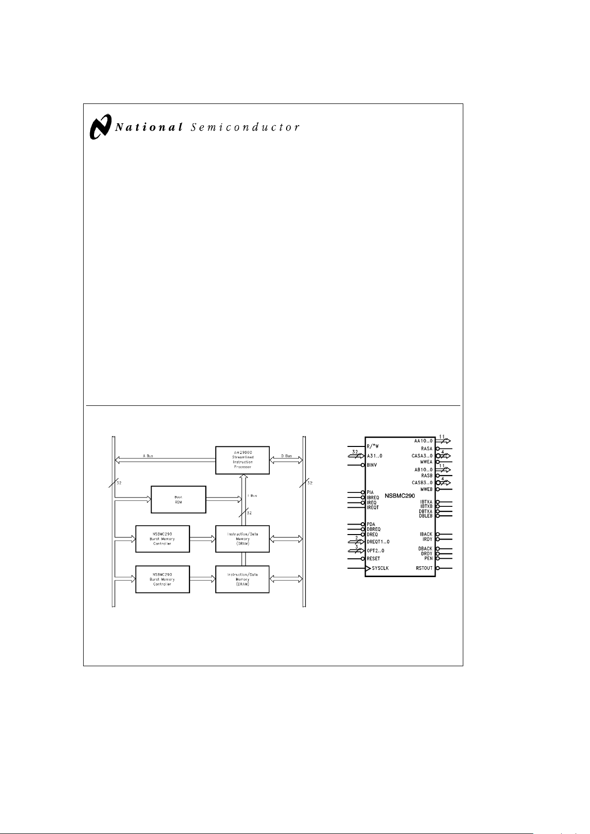
Block Diagram
Typical System Configuration
TL/V/11803– 1
Logic Symbol
TL/V/11803– 2
This document contains information concerning a product that has been developed by National Semiconductor Corporation/V3 Corporation. This information
is intended to help in evaluating this product. National Semiconductor Corporation/V3 Corporation reserves the right to change and improve the specifications
of this product without notice.
TRI-STATEÉis a registered trademark National Semiconductor Corporation.
NSBMC290
TM
is a trademark of National Semiconductor Corporation.
V29BMC
TM
is a trademark of V3 Corporation.
Am29000
TM
is a trademark of Advanced Micro Devices, Sunnyvale, California, USA.
C
1995 National Semiconductor Corporation RRD-B30M115/Printed in U. S. A.
Page 2
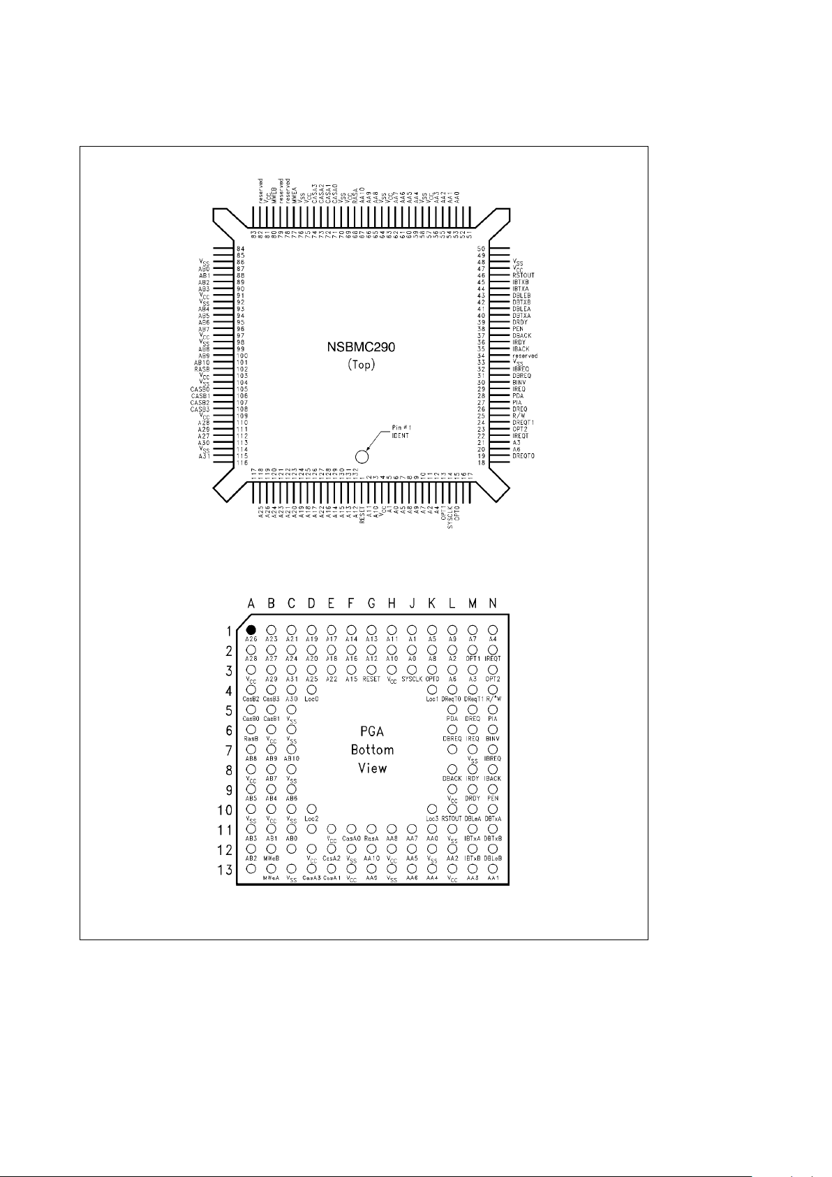
Connection Diagrams
TL/V/11803– 3
PQFP
Order Number NSBMC290VF
NS Package Number VF132A
TL/V/11803– 9
PGA Bottom View
Order Number NSBMC290UP
See NS Package Number UP124A
2
Page 3
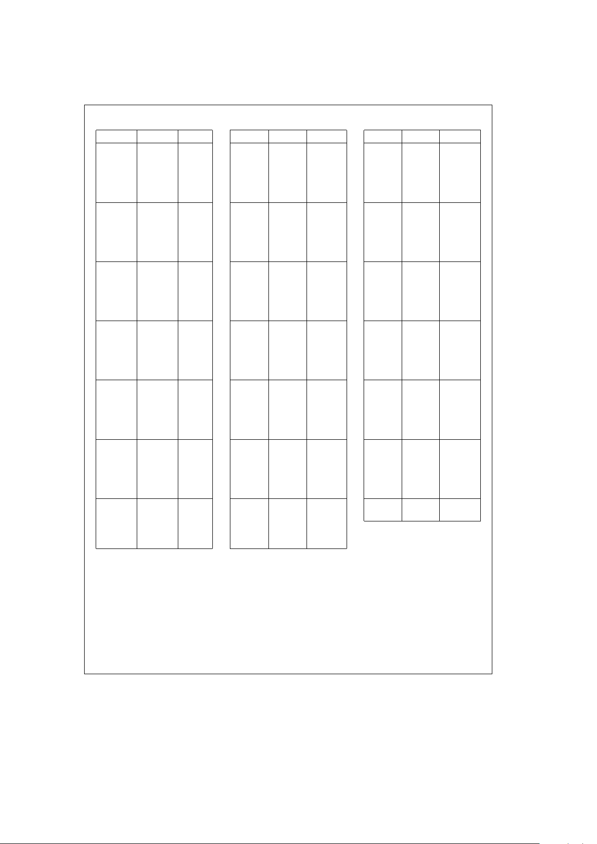
Pin Descriptions
PGA Pin QFP Pin Signal
J2 6 A0
J1 5 A1
L2 11 A2
M3 21 A3
N1 12 A4
K1 7 A5
L3 20 A6
M1 10 A7
K2 8 A8
L1 9 A9
H2 3 A10
H1 2 A11
G2 132 A12
G1 131 A13
F1 129 A14
F3 130 A15
F2 128 A16
E1 126 A17
E2 125 A18
D1 124 A19
D2 123 A20
C1 122 A21
E3 127 A22
B1 121 A23
C2 120 A24
D3 118 A25
A1 119 A26
B2 112 A27
A2 110 A28
B3 111 A29
C4 113 A30
C3 115 A31
K11 53 AA0
N13 54 AA1
L12 55 AA2
M13 56 AA3
K13 59 AA4
J12 60 AA5
J13 61 AA6
J11 62 AA7
H11 65 AA8
PGA Pin QFP Pin Signal
G13 66 AA9
G12 67 AA10
C11 87 AB0
B11 88 AB1
A12 89 AB2
A11 90 AB3
B9 93 AB4
A9 94 AB5
C9 95 AB6
B8 96 AB7
A7 99 AB8
B7 100 AB9
C7 101 AB10
N6 30 BINV
F11 71 CASA0
E13 72 CASA1
E12 73 CASA2
D13 74 CASA3
A5 105 CASB0
B5 106 CASB1
A4 107 CASB2
B4 108 CASB3
L8 37 DBACK
M10 41 DBLEA
N12 43 DBLEB
L6 31 DBREQ
N10 40 DBTXA
N11 42 DBTXB
M9 39 DRDY
M5 26 DREQ
L4 19 DREQT0
M4 24 DREQT1
N8 35 IBACK
N7 32 IBREQ
M11 44 IBTXA
M12 45 IBTXB
M8 36 IRDY
M6 29 IREQ
N2 22 IREQT
B13 77 MWEA
B12 80 MWEB
PGA Pin QFP Pin Signal
K3 15 OPT0
M2 13 OPT1
N3 23 OPT2
L5 28 PDA
N9 38 PEN
N5 27 PIA
N4 25 R/*W
G11 68 RASA
A6 102 RASB
A13 78 Reserved
C12 79 Reserved
D11 82 Reserved
L7 34 Reserved
G3 1 RESET
L10 46 RSTOUT
J3 14 SYSCLK
A3 4 V
CC
A8 47 V
CC
B6 57 V
CC
B10 63 V
CC
D12 69 V
CC
E11 75 V
CC
F13 81 V
CC
H3 91 V
CC
H12 97 V
CC
L9 103 V
CC
L13 109 V
CC
A10 33 V
SS
C5 48 V
SS
C6 58 V
SS
C8 64 V
SS
C10 70 V
SS
C13 76 V
SS
F12 86 V
SS
H13 92 V
SS
K12 98 V
SS
L11 104 V
SS
M7 114 V
SS
Note: In order for the switching characteristics of this device to be guaranteed, it is necessary to connect all of the power pins (VCC,VSS) to the appropriate power
levels. The use of low impedance wiring to the power pins is required. In systems using the Am29000 with its attendant high switching rates, multi-layer printed
circuit boards with buried power and ground planes are required.
3
Page 4

Pin Descriptions
Am29000 INTERFACE
The following pins have the same function as their counterparts on the Am29000 and are designed to be connected directly to
the Am29000 Synchronous Channel Interface.
Pin Description
A0-31 Address Bus (Input): The address bus transfers byte addresses for all accesses to the memory array except in
burst mode. The NSBMC290 can be software configured to any memory block address within the 4 Gbyte
address range.
BINV Bus Invalid (Input; Active Low): This input indicates that the address bus and related control signals are invalid.
This signal must be 0 (high) in order for the NSBMC290 to accept any data or instruction requests.
R/*W) READ/*WRITE (Input): This input indicates whether data is being transferred to the data bus (R/*W high) or to
the memory array (R/*W low).
DBACK Data Burst Acknowledge (Output; 3-State, Active Low): This output signals that burst mode accesses between
the memory array and the data bus can be continued.
DBREQ Data Burst Request (Input, Active Low): This input is used to indicate when burst mode access for data is
desired.
DRDY Data Ready (Output; 3-State, Active Low): This output is used to signal the completion of a data access cycle.
DREQ Data Request (Input; Active Low): This input signal the initiation of a memory access cycle for data.
DREQT0–1 Data Request Type (Input, Active Low): These inputs specify the address space of the data access. They must
both be 0 (low) in order for the NSBMC290 to accept a data request.
OPT0–2 Data Options (Input; Active Low): These inputs specify the data transfer size and operating mode. The
NSBMC290 responds only to cycles in which the values 0, 1, 2 are asserted. The use of these signals is
compatible with the specifications for In-Circuit Emulators.
PDA Pipelined Data Access (Input; Active Low): This input indicates that the address bus has the address for the
next data access prior to the completion of the present data request.
IBACK Instruction Burst Acknowledge (Output; 3-State, Active Low): This output signals that burst mode accesses
between the memory array and the instruction bus can be continued.
IBREQ Instruction Burst Request (Input; Active Low): This input is used to request burst mode instruction access.
IRDY Instruction Ready (Output; 3-state, Active Low): This output signals are completion of each instruction access.
IREQ Instruction Request (Input; Active Low): This input signals the beginning of an instruction access cycle.
IREQT Instruction Request Type (Input; Active High): This input specifies the address space of the instruction access.
It must be 0 (low) in order for the NSBMC290 to accept an instruction request.
PIA Pipelined Instruction Access (input; Active Low): This input indicates that the address bus has the address for
the next instruction access prior to the completion of the present instruction request.
PEN Pipeline Enable (Output; 3-State, Active Low): This output indicates that the NSBMC290 is capable of
accepting the address for the next access before completion of the present access.
RESET Reset (Input; Active Low): This input initializes the NSBMC290 to accept the software configuration information.
If more than one NSBMC290 is used for controlling memory, the NSBMC290 chips should be daisy chained with
RSTOUT from one NSBMC290 chip connecting to RESET of the next NSBMC290 Chip.
RSTOUT Reset Out (Output; Active Low): This output is active (low) whenever RESET is active and remains active until
the NSBMC290 has been software configured.
SYSCLK System Clock (Input): This input is used to synchronize the NSBMC290 to the Am29000 local channel interface.
4
Page 5
Pin Descriptions (Continued)
MEMORY INTERFACE
The NSBMC290 is designed to drive a memory array organized as 2 banks each of 32 bits. The address and control
signals for the memory array are output through high current
drivers in order to minimize the propagation delay due to
memory input impedance and trace capacitance. External
array drivers are not required. The address and control signals, however, must be externally terminated.
Pin Description
A(A,B)0–10 Multiplexed Addresses (Output; High Current): These two buses transfer the multiplexed row and column
addresses to the memory array banks A and B respectively.
RAS(A,B) Row Address Strobes (Output; High Current, Active Low): These signals are strobes that indicate the
existence of a valid row address on A(A,B)0–10. These signals are to be connected to the two interleaved banks
of memory. One is assigned to each bank.
CAS(A,B)0-3 Column Address Strobe (Output; High Current, Active Low): These signals are strobes that indicate a valid
column address on A(A,B)0–10. A set of each of these (A,B) are assigned to each memory bank, and within each
set, one is assigned to each byte of the 32-bit memory.
MWE(A,B) Memory Write Enable (Output; High Current, Active Low): These signals are the write strobes for the DRAM
memories. One is supplied for each of the two banks of memory although they are logically identical.
BUFFER CONTROLS
In order not to limit system implementation strategies vis j
vis instruction and data bus organization, the NSBMC290
permits the designer to keep these busses separate or not
as performance criteria dictate. In order to maintain bus
separation, data buffers are required. In order to maximize
performance, these buffers are controlled directly by the
NSBMC290.
Pin Description
DBLE(A,B) Data Bus Latch Enable A and B (Output; Active High): These outputs are used to enable transparent latches to
latch data from the Processor data bus to each bank of memory during a write cycle (Data access only).
The following buffer control outputs are multi-mode signals. The signal names, as they appear on the logic symbol,
are the default signal names (Mode
e
0). A more complete description is presented in the configuration section.
DBTX(A,B) Data Bus Transmit A and B (Output; Active Low): These outputs are used during read cycles to enable data
from the individual banks of memory to drive the data bus.
IBTX(A,B) Instruction Bus Transmit A and B (Output; Active Low): These outputs are used during instruction cycles to
enable data from the individual banks of memory to drive the instruction bus.
5
Page 6
Functional Description
PRODUCT OVERVIEW
The NSBMC290 is designed to simplify the interface between the Am29000 high-speed synchronous channel and
dynamic memories. This integrated circuit responds to all
defined instruction and data access modes of the Am29000,
and handles all required address decoding and multiplexing
for the DRAM memory array. In addition, the NSBMC290
automatically generates refresh cycles to the memory array.
Software configuration is used to setup the memory block
address, refresh rate, byte order, bus buffer control type and
DRAM memory chip size parameters for the NSBMC290. If
two or more memory blocks are used to implement an
Am29000 memory sub-system, the processor can simultaneously access one memory block via the data bus and a
second memory block via the instruction bus. If both accesses are directed to the same memory block, the
NSBMC290 will hold off the second access until the first
has completed; only then will it process the second access.
SYSTEM INTERFACE
The NSBMC290 connects directly to the Am29000 address
bus, instruction and data bus controls signals. The interface
handles simple, pipelined and burst mode access for both
the data and instruction bus, according to the Am29000
channel specification. It requires no external logic to implement the synchronous channel connection. Thus, it avoids
the propagation delays and signal skews that can detract
from system performance and increase system complexity.
MEMORY INTERFACE
The NSBMC290 directly drives an array of DRAM devices
which can support page mode accesses. The array is organized as 2 banks of 32 bits each. The supported devices are
all the standard memory size from 64 Kbit to 16 Mbit. Selection of the device in use is done via software.
During burst accesses, the NSBMC290 executes interleaved page mode accesses to 2 banks. This allows the
memory to run at the full processor speed of 1 memory
cycle per processor cycle. For data accesses, the
NSBMC290 controls the memory as four independent of
8-bit bytes in order to allow 8-, 16- and 32-bit accesses.
The byte order for interpreting the byte address is software
configurable. However, the NSBMC290 does not detect if
the access overflows a word boundary. The software operating on the Am29000 should manage the correct alignment
for memory accesses that are not word aligned. Systems
using Am29000 processors whose revision level is previous
to Revision ‘‘C’’ must manage alignment of byte data
through software so that the data will retain correct justification.
The NSBMC290 allows for flexibility in the control of instruction and data buffers for the memory array. Propagation delay is minimized by providing these controls directly, and by
allowing the control strategy to be software programmable.
For example 74F245 or high current Am29861 bus buffers
may be used without external ‘‘glue’’ circuitry.
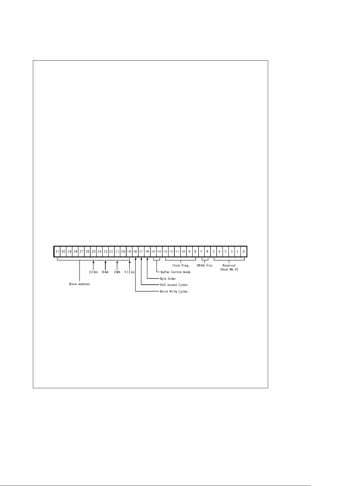
CONFIGURATION
The NSBMC290 is configured by the first 32-bit memory
read access following deassertion of the RESET signal. If
multiple NSBMC290 devices are used in a circuit, they
should be daisy chained together with RSTOUT from one
chip connecting to RESET of the next chip. When a
NSBMC290 has been configured, it deasserts the RSTOUT
signal allowing the next NSBMC290 in the chain to then be
configured. All NSBMC290 devices must be configured before memory accesses are attempted.
TL/V/11803– 4
FIGURE 1. NSBMC290 Configuration Word
6
Page 7

Functional Description (Continued)
BLOCK ADDRESS
Once configured, a NSBMC290 only responds to addresses
within the block address range configured. The programmed value corresponds to the starting address of the
block, while the size of the block is determined by the size
of the devices used. For example, if 1M x 1 DRAM devices
are selected, the memory block size is 8M bytes and is always located on an 8M byte boundary.
Figure 1
shows the
least significant bit of the block address for each block size.
BYTE ORDER
When bit 16 of the configuration word is set to 0, the convention used for numbering sequential bytes in a word is
that byte address 0 selects bits 0 – 7, byte address 1 selects
bits 8–15 and so on. If bit 16 of the configuration word is set
to 1, this ordering is reversed and byte address 0 selects
24–31 etc. The bit order of data within a byte is unaffected
by the byte order selected. This feature facilitates the implementation of multi-processor systems in which programmable Big/Little Endian byte order is not supported by all processors.
BURST WRITE CYCLES
The NSBMC290 supports instruction and data reads at a
rate of one access per SYSCLK cycle during bursts. However, the flexibility of the data buffer strategy is such that buffer and memory device combinations may be selected for
which the data hold time during single clock write cycles
cannot be guaranteed across all system operating conditions of temperature and voltage. A two clock write cycle
has thus been provided in order to support these combinations. Configuration Bit 18 is set to 0 if a two clock data
burst write cycle is required, 1 if single clock write cycle is
possible. The NSBMC290 Application Guide details the factors that influence the selection of this parameter.
RAS ACCESS CYCLES
To maximize the choice of memory device speeds that may
be used with various system clock rates, the NSBMC290
can be configured such that the Row Address Strobe (RAS)
period lasts for either 3 or 4 clock periods during simple
accesses. When set to 1, configuration bit 17 indicates that
3 clock cycles are to be used, when set to 0, 4 are required.
Calculation of the number of cycles required is detailed in
the NSBMC290 Application Guide.
BUFFER CONTROL MODES
The combination of programmable RAS period and burst
write cycle duration permit the system designer to trade
memory device speed and organization in order to optimize
system performance, cost, and storage capacity. This flexibility is further enhanced by providing multiple methods of
buffering the memory sub-system and the Am29000 Local
Channel.
TABLE I. Interpretation of the Buffer Control
Signals for Various Control Modes
Modes Bits Signal 1 Signal 2 Signal 3 Signal 4
00 DBTxA DBTxB IBTxA IBTxB
01 DBCeA DBCeB IBTxA IBTxB
10 DBTx BankB/*A IBTx IBTx
11 DBCe BankB/*A IBTx IBTx
Note: The mode 00 signal names are the defaults used for reference purposes.
The transfer of Instructions and Data from the memory subsystem to the Local Channel occurs through buffers controlled by the NSBMC290. Of the six signals provided for
this purpose, four operate in multiple modes; the remaining
two (DBLeA, DBLeB) have fixed interpretation. These two
signals provide latch enable controls for transparent latches
for use during data transfers from the Am29000 to memory.
The functions performed by the remaining four signals
change according to the programmed mode. Table I presents these signals using names that are function derived.
Signals with a DB prefix are used to control Data Bus operations while those starting with IB control instruction bus operations. Signals containing TX are Buffer transmit controls
which are typically used with buffers that have output enables (transmit relative to the memory system). Buffers such
as 74F245 or 74F646 which have direction and enable pins
are controlled with a CE (chip enable) signal (DBCE,
DBCEa, DBCEb).
Signals ending with A or B are specific to one or the other of
the two interleaved banks of memory controlled by the
NSBMC290; signals without suffixes apply to both banks.
The signal BankB/*A, required in some configurations, indicates which DRAM memory bank will be next selected.
7
Page 8

Functional Description (Continued)
TABLE II. Buffer Control Signals and the Memory Bank for Which they are active
Simple/Pipeline Cycle Burst Cycle
Signal Name Read Write Read Write
DBTX A,B A,B (Note 1)
DBTXa A A (Note 2)
DBTXb B B (Note 2)
DBCE A,B A,B A,B (Note 1) A,B (Note 1)
DBCEa A A A (Note 2) A, B (Note 1)
DBCEb B B B (Note 2) A,B (Note 1)
IBTX A,B A,B (Note 1)
IBTXa A A (Note 2)
IBTXb B B (Note 2)
BankB/*A (Note 3) 1eMemory Bank B is next active, 0eBank A is next
Note 1: Remains active over the entire burst cycle regardless of the bank being accessed.
Note 2: Asserted only when the specific bank is being accessed.
Note 3: Must be externally synchronized to SYSCLK.
The memory buffer strategy required will depend on the
type of DRAMs being used (bit wide vs nibble wide components), the access time of these memories, the desired
burst write speed, and the system clock speed. Table III
presents some of the possible configurations with the corresponding mode settings. For a comprehensive discussion of
the selection of a buffer strategy, lease refer to the
NSBMC290 Application Guide. This document expands the
rationale of the selection process and presents specific application examples and circuit diagrams.
TABLE III. Possible NSBMC290
Memory/Buffer Configurations
Buffer Type
DRAM Burst BMC
Organization Write Buffer Mode
74F245 Nibble 2 Cycle Mode 3
74F245 Bit 2 Cycle Mode 1
74F245, 74F646 Nibble 1 Cycle Mode 3
74F245, 74F646 Bit 1 Cycle Mode 1
Am29C983 Bit 1 Cycle Mode 2
29827, 29861 Bit 2 Cycle Mode 0
SYSTEM CLOCK FREQUENCY
The system clock frequency is used to derive the period of
DRAM refresh cycles. The refresh rate is given by (system
clock frequency)/(16 x (programmed value
a
1)). This meets
the nominal refresh requirements for DRAM devices. For
example, if the system clock is 25 MHz and the programmed value is 24, the NSBMC20 will execute the 256
refresh cycles for a 256k DRAM in 4.096 ms. Bit 13 of the
configuration word in the MSB of the frequency field while
bit 8 is the LSB. The refresh algorithm employed by the
NSBMC290 guarantees the time for complete device refresh, however, the time for individual row refreshes may be
held off to prevent the preemption of a burst.
DRAM SIZE
This two bit field, bit 7 and bit 6, configures the NSBMC290
for the correct memory address size, and hence total memory block size. Note that the memory in both banks of the
block are required to be of the same size, and organization
in order for correct operation to occur. Table IV lists the
supported device sizes.
TABLE IV. Size Code Settings, DRAM
Density and Address Range Size
Memory
DRAM Memory
Size Code
Address Size Block Size
(in Bits 7, 6)
0 64kBx164kBx4 512KBytes
1 256 kB x 1 256 kB x 4 2 MBytes
2 1MBx11MBx4 8MBytes
3 4MBx14MBx4 32MBytes
8
Page 9

Functional Description (Continued)
INTERCONNECT DETAILS
The NSBMC290 may be applied in designs where instruction and data memories are separated or in designs where
a single memory space is used for both instruction and data.
In split instruction/data designs, the control signals for the
address space not required are simply pulled up to V
CC
levels and not connected to the corresponding local channel signals.
TABLE V. Control Signal Set Unique
to Instruction Accesses
Signal Type Signal Names
Input IREQ, IBREQ, IREQT, PIA
Output IBACK, IRDY
Buffer Control IBTXA, IBTXB, IBTX, BANKB/*A
TABLE VI. Control Signal Set Unique to Data Accesses
Signal Type Signal Names
Input DREQ, DBREQ, DREQT[1..0],
OPT[2..0]PDA
Output DBACK, DRDY
Buffer Control DBCEA,B, DBCE, DBTXA,B,
DBTX, BANKB/*A
For mixed instruction and data designs, all local channel
signals must be connected. Tables V and VI detail the control signal sets required for the NSBMC290 to control the
corresponding address spaces. It is recommended that all
control signals be connected and that instruction and data
space segregation be done via software allocation and/or
use of the Am29000 internal Translation Look-Aside Buffer.
Typical Application
SYSTEM IMPLEMENTATION AND DESIGN
The ease with which the NSBMC290 may be integrated into
a system design is illustrated in the diagram in
Figure 2
. The
system shown supports an Am29000 with between 2 MB
and 32 MB of memory (depending on the storage devices
selected) managed by a single NSBMC290. This specific
example accommodates 256k x 1, 1 MBx1or4MBx1
devices.
In a minimal system configuration only one NSBMC290 is
required. This is because the NSBMC290 manages both instruction and data access to a memory block. However, with
a single memory block, instruction and data accesses cannot be overlapped and the number of burst access restarts
is a function of the way in which the software is designed. It
is therefore difficult to predict performance degradation.
If maximum performance is required, the addition of one or
more NSBMC290s is an effective solution. Our bench marks
indicate that for systems with physically separated instruction and data space performance is degraded by approximately 5% over the theoretical rate achieved in system designs employing high speed static RAMs. The device count
and cost of these solutions, however, differ by at least a
factor of 6.
With the exception of data buffers external components are
not required, except to terminate the address and control
lines to the memory array. The use of passive components
arranged in a serial or parallel terminating network is a simple but effective method of implementing this requirement.
9
Page 10

Typical Application (Continued)
TL/V/11803– 5
FIGURE 2. Possible System Interconnection Using the NSBMC290
10
Page 11

CPU INTERFACE
The NSBMC290 interface to the Am29000 has been designed for direct interconnect. Normally it is not necessary
to place other logic devices between the processor,
NSBMC290, and memory with the exception of Instruction/
Data bus buffers. The introduction of intermediate buffers
can result in skews or delays that will require that the system clock frequency be derated for operation under worst
case conditions.
SIMPLE ACCESS SEQUENCE
The NSBMC290 can return data to the processor in only 4
clocks or 5 clocks for a simple access depending on the
mode chosen (Configuration Bit 17). If multiple access
cycles are requested back to back, then the BMC will pause
for a minimum of 2 clocks between RAS cycles to insure
that the RAS precharge time is met resulting in 5 clocks or 6
clocks between successive simple cycles (depending on
Configuration bit 17).
All access modes begin their cycle in the same fashion as a
simple access. A simple access can become either a pipelined or burst access if the appropriate inputs are driven.
Figure 3 shows the timing relationship between the system
clock, processor control signals and NSBMC290 outputs.
All NSBMC290 outputs are derived synchronously with the
exception of t
ARA
7
(processor address to memory address
delay). The shaded section in Figure 3 represents the extra
cycle inserted when the configuration register is initialized
with bit 17 cleared.
TL/V/11803– 6
²
DBTX, DBTXa, DBTXb, DBCE, DBCEa, DBCEb, IBTX, IBTXa, IBTXb
FIGURE 3. Simple Access Sequence
11
Page 12

Typical Application (Continued)
TL/V/11803– 8
FIGURE 4. Burst Read Sequence (Illustrating Burst Suspension)
BURST ACCESS SEQUENCE
When Burst access has been established, the NSBMC290
generates the signal sequence of
Figure 5
. This access sequence will continue until either canceled or suspended by
the Am29000 or normal burst termination occurs. The
NSBMC290 will preempt the burst sequence only in the
case that a refresh cycle has been requested, and has been
outstanding for a time in excess of 80% of the refresh period.
FUNCTIONAL OVERVIEW OF BURST ACCESS
Figure 4
diagrams the sequence of events that take place
during a typical burst sequence. This specific example describes the operations surrounding instruction or data reads.
The example illustrates how burst operation is established,
suspended for a cycle, and subsequently terminated by the
master.
The sequence commences at T
0
when the NSBMC290 is
selected. Once selected, the BMC drives RAS of the memory bank which contains data for the initial access of the
burst cycle (Bank A in this case). During the next period
(T
1
), CASa is asserted and the RAS for the other memory
bank (RASb) is activated. Access to the second memory
bank is offset by one cycle in order that bank interleave will
occur correctly.
The first word of data is available to the processor by T
3
as
indicated by RDY asserted. Data from the memory must
propagate through any data buffers and meet the setup time
of the 29k processor by T
3
. An extra cycle is inserted into
the start-up phase of the burst sequence if bit 17 of the
configuration register is programed to ‘‘0’’. This increases
the RAS assertion time from 3 cycles to 4 cycles. The resulting delay is inserted during T
2
.
12
Page 13

Absolute Maximum Ratings
If Military/Aerospace specified devices are required,
please contact the National Semiconductor Sales
Office/Distributors for availability and specifications.
Supply Voltage (V
CC
)
b
0.3V toa7V
Input Voltage (VIN)
b
0.3V to V
CC
a
0.3V
DC Input Current (I
IN
)
g
50 mA
Storage Temperature (T
STG
)
b
65§Ctoa150§C
Recommended Operating
Conditions
Supply Voltage (VCC) 4.75V to 5.25V
Ambient Temperature (TA)
Plastic Package 0
§
Ctoa70§C
Ceramic Package
b
55§Ctoa85§C
DC Electrical Characteristics
Symbol Description Conditions Min Max Units
V
IL
Low Level Input Voltage V
CC
e
4.75V 0.8 V
V
IH
High Level Input Voltage V
CC
e
5.25V 2.0 V
I
IL
Low Level Input Current V
IN
e
VSS,V
CC
e
5.25V
b
10 mA
I
IH
High Level Input Current V
IN
e
V
CC
e
5.25V 10 mA
V
OL
Low Level Output Voltage V
IN
e
VILor V
IH
0.4
V
I
OL
e
24 mA
V
OH
High Level Output Voltage V
IN
e
VILor V
IH
3.7
V
I
OL
e
24 mA
I
OZL
Low Level TRI-STATE
É
V
IN
e
VILor V
IH
b
20
mA
Output Current V
O
e
V
SS
I
OZH
Low Level TRl-STATE V
IN
e
VILor V
IH
20
mA
Output Current V
O
e
5.25V
I
CC(Max)
Maximum Supply Current Continuous Simple Access 100
mA
Continuous Burst Access 30
C
IN
Input Capacitance 20 pF
C
OUT
Output Capacitance 20 pF
13
Page 14

Timing Parameters
TL/V/11803– 10
²
DBTX, DBTXa, DBTXb, DBCE, DBCEa, DBCEb, IBTX, IBTXa, IBTXb
FIGURE 5. Simple Access Timing
14
Page 15

AC Timing Parameters (Unless otherwise stated V
CC
e
5.0Vg5%, 0§CkT
A
k
70§C.)
Ý
Symbol Description
16 MHz 20 MHz 25 MHz 33 MHz
Units
Min Max Min Max Min Max Min Max
1t
BSU
BlNV Setup 8 7 6 5 ns
2t
BH
BINV Hold 4 3 3 2 ns
3t
RQSU
Request Sync. Setup Time 17 13 12 10 ns
4t
RQH
Request Sync. Hold Time 4 3 3 2 ns
5t
SU
Synchronous Input Setup 17 13 12 10 ns
5A t
SU
Synchronous Input Setup I/DBREQ only 9 8 6 4.5 ns
6t
H
Synchronous Input Hold 4 3 3 2 ns
6A t
BRH
*SYSCLK to Burst Request Input Hold 4 3 3 2 ns
7t
ARA
Address Input to Row Address output delay 29 24 22 18 ns
(Note 1)
8t
RAH
*SYSCLK to row address hold 9 8 7 6 ns
8A t
DRAH
DRAM Row Address Hold (Note 2) t
CLK
-4 t
CLK
-4 t
CLK
-3 t
CLK
-2 ns
9t
CAV
*SYSCLK to Column Address Valid Delay 38 32 29 24 ns
(Note 1)
10 t
CAH
SYSCLK to Column Address Hold 6 6 5 5 ns
11 t
RSHL
SYSCLK to RAS Asserted Delay (Note 1) 26 22 20 17 ns
12 t
RSLH
SYSCLK to RAS De-asserted Delay (Note 1) 23 19 17 14 ns
13 t
CHL
SYSCLK to CAS Asserted Delay (Note 1) 32 27 24 20 ns
14 t
CLH
SYSCLK to CAS De-asserted (Note 1) 40 33 30 25 ns
15 t
PZH
PEN 3-state to Valid Delay Relative to 30 25 23 19 ns
*SYSCLK
16 t
PHL
PEN Synchronous Assertion Delay 26 22 20 17 ns
17 t
PLH
PEN Synchronous Deassertion Delay 25 21 19 16 ns
18 t
PHZ
PEN Valid to 3-state Delay Relative to 29 24 22 18 ns
*SYSCLK
19 t
RZH
RDY 3-state to Valid Delay Relative to 30 25 23 19 ns
*SYSCLK
20 t
RHL
RDY Synchronous Assertion Delay 26 22 20 17 ns
21 t
RLH
RDY Synchronous De-assertion Delay 25 21 19 16 ns
22 t
RHZ
RDY Valid to 3-state Delay Relative to 29 24 22 18 ns
*SYSCLK
23 t
LEHL
Synchronous Latch Enable Assertion delay 32 27 24 20 ns
24 t
LELH
Synchronous Latch Enable De-assertion Delay 42 35 32 26 ns
25 t
BHL
Synchronous Buffer Enable Assertion Delay 49 41 37 31 ns
26 t
BLH
Synchronous Buffer Enable De-assertion Delay 38 32 29 24 ns
27 t
RWSU
Synchronous R/*W Input Setup Time 8 7 6 5 ns
28 t
RWH
Synchronous R/*W Input Hold Time 4 3 3 2 ns
29 t
WEV
Synchronous Write Enable Valid Delay 59 49 44 37 ns
Relative to *SYSCLK
30 t
BKZH
Synchronous I/DBACK Valid Delay 25 21 19 16 ns
31 t
BKHL
Synchronous I/DBACK Assertion Delay 29 24 22 18 ns
32 t
BKLH
Synchronous I/DBACK Deassertion Delay 24 20 18 15 ns
33 t
BKHZ
Synchronous I/DBACK Valid to 3-state Delay 24 20 18 15 ns
34 t
ABKLH
Asynchronous I/DBACK Deassertion delay 22 18 14 12 ns
relative to I/DREQ
*Signal output delays are measured relative to SYSCLK (except as indicated) using a 50 pF load.
Note 1: Derate the given delays by 0.06 ns per pF of load in excess of 50 pF.
Note 2: Where t
CLK
e
1/(2 * Clock Frequency)
15
Page 16

AC Timing Parameters (Continued)
TL/V/11803– 7
²
TXaeIBTXa, DBTXa; CEaeIBCEa, DBCE; TXbeIBTXb, DBTXb; CEbeIBCEb, DBCEb and BANKb/*a.
Note: Buffer control signal timing is illustrated using the mode dependent signal naming convention. (See page 7.) As shown, the switching behavior is typical of
modes 0 and 1. In modes 2 and 3 the timing of signals DBTX, DBCE and IBTX remain unchanged.
FIGURE 6. Burst Access Timing
TABLE VIII. Burst Access Timing Parameters
Ý
Symbol Description
16 MHz 20 MHz 25 MHz 33 MHz
Units
Min Max Min Max Min Max Min Max
1t
CHL
*SYSCLK to CAS Assertion (Note 1) 25 21 19 15.5 ns
2t
CLH
SYSCLK to CAS De-Assertion (Note 1) 24 20 18 15 ns
3t
CAV
*SYSCLK to Column Address Valid Delay (Note 1) 38 32 29 24 ns
4t
CAH
*SYSCLK to Column Address Hold Time (Note 1) 6 34 5 28 5 25 3 21 ns
5t
BHL
SYSCLK to Buffer Control Assertion Delay 25 21 19 15.5 ns
6t
BLH
*SYSCLK to Buffer Control De-Assertion Delay 24 20 18 15 ns
7t
LEHL
*SYSCLK to Latch Enable Assertion 26 22 20 16.5 ns
8t
LELH
SYSCLK to Latch Enable De-Assertion 26 22 20 16.5 ns
*Signal output delays are measured relative to SYSCLK (except as indicated) using a 50 pF load.
Note 1: Derate given the delays by 0.06 ns per pF or load in excess of 50 pF.
16
Page 17

Release Notes for NSBMC290
Revision ‘‘A’’
A NOTE ON THE OPERATION OF THE Am29000
It is a characteristic of the Am29000 (Rev D) that it can deassert the *IBREQ signal independently of the current state
of *IRDY and *IBACK. The V29BMC (Rev A) accommodates this behavior in all cases with one exception.
ERRATUM
Ý
1
If *IBREQ is de-asserted 1 or two clock cycles before
*IRDY is returned and the instruction access cycle is fol-
lowed in the next clock cycle by a data write, the write enable signals from the V29BMC to memory are asserted (/2
clock cycle before *RAS/*CAS are de-asserted. The memory location following the last completed instruction access
may be corrupted.
RECOMMENDED FIX
The ‘‘write enables’’ to memory must be delay by a clock
cycle. This may be achieved in the following ways:
1. The *RAS signals may be used to latch the write enable
from the V29BMC as shown in
Figure 7
.
2. The write enable into the V29BMC may be delayed. See
Figure 8.
TL/V/11803– 11
FIGURE 7
The logic shown in
Figure 7
can be implemented in a PAL
using the following positive true logic equation:
WEa
e
!RASa & MWE
Ý
RASa & WEA;
MWE is MWEa or MWEb since they are identical.
TL/V/11803– 12
FIGURE 8
The PAL shown in
Figure 8
can be programmed with one of
the two following equations depending on which of the two
dotted paths is connected:
RDÐONLY.d
e
RASa & RASb & BMCÐR/W;
or
RDÐONLY.d
e
RASa & RASb & IREQ;
The primary difference between the two recommended solutions is that the one given in
Figure 8
makes use of the
high current drivers on the V29BMC for driving the write
enable signal to the memory array. For systems using bit
organized memories, this type of drive capability is desired.
The ‘‘or’’ function implemented by the ’F32 may be moved
inside the PAL by appropriately modifying the equations. For
maximum performance, it should be a discrete gate as
shown.
This modification is only required for a V29BMC controlling
memories from which instructions are being run. This modification, however implemented, will affect the timing of Pipeline Cycles. Do not connect PEN to a V29BMC whose write
timing is modified, and connect PIA, PDA only to a pull-up
resistor. For a V29BMC controlling data only memory, no
changes to the write enable timing are required and pipeline
access may be used. Using data pipelining, performance
improvements of the order of 2% have been observed.
ERRATUM
Ý
2
If buffer mode 3 (or 1) is selected, then it is possible for
*DBCE(a,b) to be asserted during a refresh cycle. This will
happen if a data write cycle not accessing the BMC is followed in the next cycle by a read cycle also not accessing
the BMC such that refresh on the BMC starts with the read.
The result is that the data bus can be driven by the buffers
controlled by the V29BMC when other devices are using it.
RECOMMENDED FIX
There are a number of possible fixes of which 2 are outlined
below. The first solution is to use the mode 2 (or 0) buffer
control signals and generate a *DBCE(a,b) signal from
*WE(a,b) and *DBTX(a,b). Make sure that mode 2(or 0) operation is selected in the V29BMC configuration word.
TL/V/11803– 13
FIGURE 9. Generation of *DBCE
from *WE and *DBTX Signals
The second solution is to use the DBCE(a,b) signal and
qualify it using the DBLE signals as shown below.
TL/V/11803– 14
FIGURE 10. Modification of *DBCE Signal
Using the V29BMC Latch Enable Signals
17
Page 18

Ordering Code Information
NS BMC 290 UP - 33
National Semiconductor Frequency
16 MHz
Mode
20 MHz
Burst Mode Controller
25 MHz
33 MHz
Processor
290
e
AMD 29000 Family
Packaging
UP
e
124-Lead PPGA
VF
e
132-Lead PQFP
18
Page 19

Physical Dimensions inches (millimeters)
Pin Grid Array (PGA)
Order Number NSBMC290UP
NS Package Number UP124A
19
Page 20

NSBMC290-16/-20/-25/-33 Burst Mode Memory Controller
Physical Dimensions inches (millimeters) (Continued)
Plastic Quad Flatpak (PQFP)
Order Number NSBMC290VF
NS Package Number VF132A
LIFE SUPPORT POLICY
NATIONAL’S PRODUCTS ARE NOT AUTHORIZED FOR USE AS CRITICAL COMPONENTS IN LIFE SUPPORT
DEVICES OR SYSTEMS WITHOUT THE EXPRESS WRITTEN APPROVAL OF THE PRESIDENT OF NATIONAL
SEMICONDUCTOR CORPORATION. As used herein:
1. Life support devices or systems are devices or 2. A critical component is any component of a life
systems which, (a) are intended for surgical implant support device or system whose failure to perform can
into the body, or (b) support or sustain life, and whose be reasonably expected to cause the failure of the life
failure to perform, when properly used in accordance support device or system, or to affect its safety or
with instructions for use provided in the labeling, can effectiveness.
be reasonably expected to result in a significant injury
to the user.
National Semiconductor National Semiconductor National Semiconductor National Semiconductor
Corporation Europe Hong Kong Ltd. Japan Ltd.
1111 West Bardin Road Fax: (
a
49) 0-180-530 85 86 13th Floor, Straight Block, Tel: 81-043-299-2309
Arlington, TX 76017 Email: cnjwge@tevm2.nsc.com Ocean Centre, 5 Canton Rd. Fax: 81-043-299-2408
Tel: 1(800) 272-9959 Deutsch Tel: (
a
49) 0-180-530 85 85 Tsimshatsui, Kowloon
Fax: 1(800) 737-7018 English Tel: (
a
49) 0-180-532 78 32 Hong Kong
Fran3ais Tel: (
a
49) 0-180-532 93 58 Tel: (852) 2737-1600
Italiano Tel: (
a
49) 0-180-534 16 80 Fax: (852) 2736-9960
National does not assume any responsibility for use of any circuitry described, no circuit patent licenses are implied and National reserves the right at any time without notice to change said circuitry and specifications.
 Loading...