

Page 1
TL/V/11805
NSBMC096-16/-25/-33 Burst Memory Controller
August 1993
NSBMC096-16/-25/-33 Burst Memory Controller
General Description
The NSBMC096 Burst Memory Controller is an integrated
circuit which implements all aspects of DRAM control for
high performance systems using an i960
É
CA/CF
SuperScalar Embedded Processor. The NSBMC096 is functionally equivalent to the V96BMC
TM
.
The extremely high instruction rate achieved by these processors place extraordinary demands on memory system design if maximum throughput is to be sustained and costs
minimized.
Static RAM offers a simple solution for high speed memory
systems. However, high cost and low density make this an
expensive and space consumptive choice.
Dynamic RAMs are an attractive alternative with higher density and low cost. Their drawbacks are, slower access time
and more complex control circuitry required to operate
them.
The access time problem is solved if DRAMs are used in
page mode. In this mode, access times rival that of static
RAM. The control circuit problem is resolved by the
NSBMC096.
The function that the NSBMC096 performs is to optimally
translate the burst access protocol of the i960 CA/CF to the
page mode access protocol supported by dynamic RAMs.
The device manages one or two-way interleaved arrangements of DRAMs such that during burst access, data can be
read, or written, at the rate of one word per system clock
cycle.
The NSBMC096 has been designed to allow maximum flexibility in its application. The full range of processor speeds is
supported for a wide range of DRAM speeds, sizes and organizations.
No glue logic is required because the bus interface is customized to the i960 CA/CF. System integration is further
enhanced by providing a 24-bit heartbeat timer and a bus
watch timer on-chip.
The NSBMC096 is packaged as a 132-pin PQFP with a footprint of only 1.3 square inches. It reduces design complexity, space requirements and is fully derated for loading, temperature and voltage.
Features
Y
Interfaces directly to the i960 CA
Y
Integrated Page Cache Management
Y
Manages Page Mode Dynamic Memory devices
Y
On-chip Memory Address Multiplexer/Drivers
Y
Supports DRAMs trom 256 kB to 64 MB
Y
Bit counter/timer
Y
Non-interleaved or two way interleaved operation
Y
5-Bit Bus Watch Timer
Y
Software-configured operational parameters
Y
High-Speed/Low Power CMOS technology
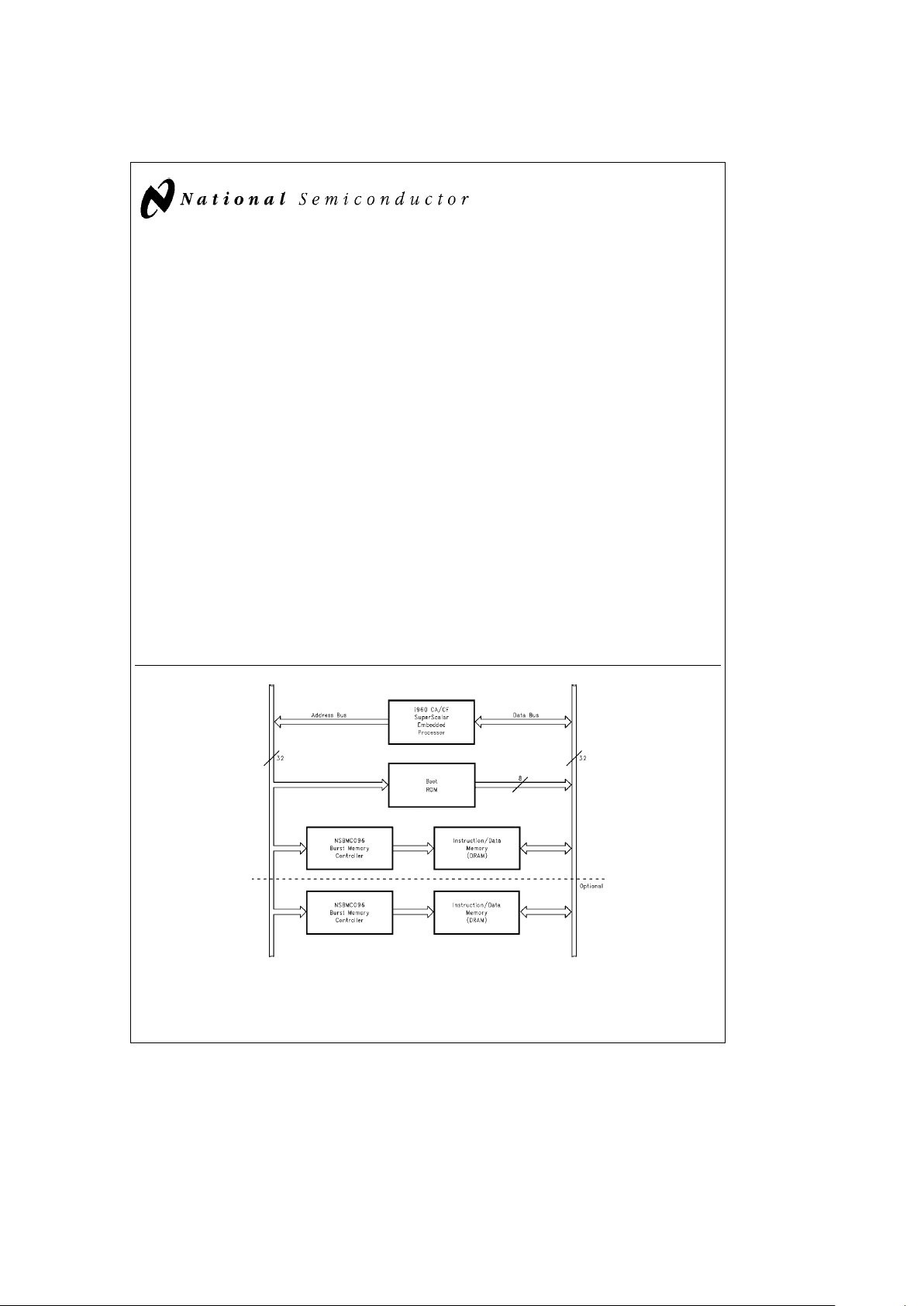
Block Diagram
TL/V/11805– 1
This document contains information concerning a product that has been developed by National Semiconductor Corporation/V3 Corporation. This information
is intended to help in evaluating this product. National Semiconductor Corporation/V3 Corporation reserves the right to change and improve the specifications
of this product without notice.
TRI-STATEÉis a registered trademark of National Semiconductor Corporation.
NSBMC096
TM
and WATCHDOGTMare trademarks of National Semiconductor Corporation.
i960
É
is a registered trademark of Intel Corporation.
V96BMC
TM
is a trademark of V3 Corporation.
C
1995 National Semiconductor Corporation RRD-B30M115/Printed in U. S. A.
Page 2
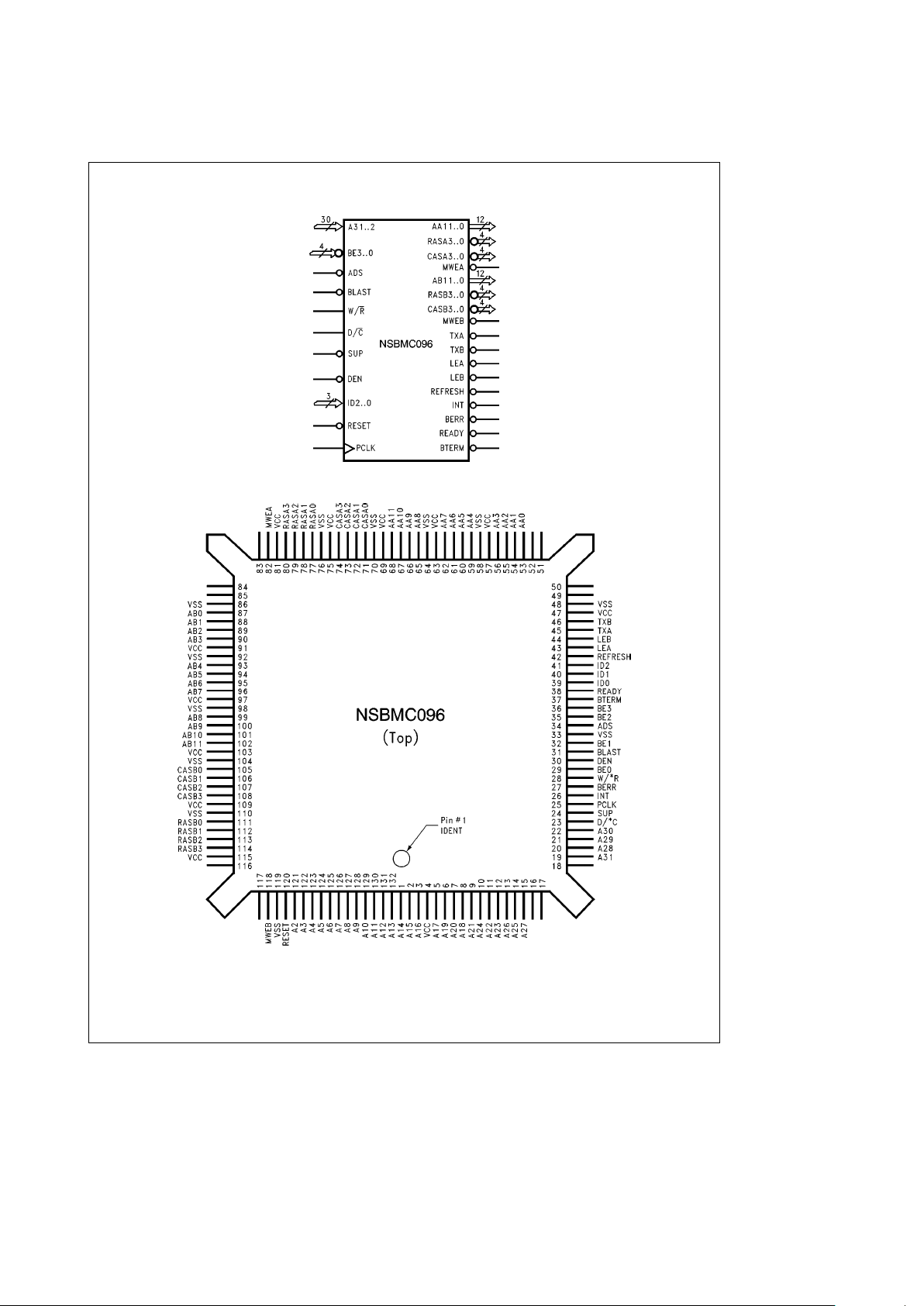
Logic and Connection Diagrams
TL/V/11805– 2
TL/V/11805– 3
Order Number NSBMC096VF
See Package Number VF132A
2
Page 3
Pin Descriptions
TABLE I
Pin
Ý
Signal Name
1 A14
2 A15
3 A16
4V
CC
5 A17
6 A19
7 A20
8 A18
9 A21
10 A24
11 A22
12 A23
13 A26
14 A25
15 A27
19 A31
20 A28
21 A29
22 A30
23 D/C
24 SUP
25 PCLK
26 INT
27 BERR
28 W/R
29 BE0
30 DEN
31 BLAST
32 BE1
33 V
SS
34 ADS
35 BE2
36 BE3
37 BTERM
38 READY
39 ID0
40 ID1
41 ID2
42 REFRESH
43 LEA
Pin
Ý
Signal Name
44 LEB
45 TXA
46 TXB
47 V
CC
48 V
SS
53 AA0
54 AA1
55 AA2
56 AA3
57 V
CC
58 V
SS
59 AA4
60 AA5
61 AA6
62 AA7
63 V
CC
64 V
SS
65 AA8
66 AA9
67 AA10
68 AA11
69 V
CC
70 V
SS
71 CASA0
72 CASA1
73 CASA2
74 CASA3
75 V
CC
76 V
SS
77 RASA0
78 RASA1
79 RASA2
80 RASA3
81 V
CC
82 MWEA
86 V
SS
87 AB0
88 AB1
89 AB2
90 AB3
Pin
Ý
Signal Name
91 V
CC
92 V
SS
93 AB4
94 AB5
95 AB6
96 AB7
97 V
CC
98 V
SS
99 AB8
100 AB9
101 AB10
102 AB11
103 V
CC
104 V
SS
105 CASB0
106 CASB1
107 CASB2
108 CASB3
109 V
CC
110 V
SS
111 RASB0
112 RASB1
113 RASB2
114 RASB3
115 V
CC
118 MWEB
119 V
SS
120 RESET
121 A2
122 A3
123 A4
124 A5
125 A6
126 A7
127 A8
128 A9
129 A10
130 A11
131 A12
132 A13
Note: In order for the switching characteristics of this device to be guaranteed, it is necessary to connect all of the power pins (VCC,VSS) to the appropriate power
levels. The use of low impedance wiring to the power pins is required. In systems using the i960 CA with its attendant high switching rates, multi-layer printed circuit
boards with buried power and ground planes are required.
3
Page 4
Pin Descriptions (Continued)
i960 CA/CF INTERFACE
The following pins are functionally equivalent to those on
the i960 CA/CF from which their names are taken. Like
named pins on the i960 CA/CF and the NSBMC960 are to
be wired together. All 3-State outputs are to be weakly
pulled up to V
CC
. In typical situations, a 10 kX resistor is
sufficient.
Pin Description
A2–31 Address Bus (Input): This system bus is a word address which determines the location at which an access is
required.
ADS Address Strobe (Input; Active Low): Indicates that a new access cycle is being started.
D/*C Data/*Code (Input): Signals whether an access is for data or instructions.
BLAST Burst Last (Input; Active Low): Indicates that the last cycle of a burst is in progress.
DEN Data Enable (Input; Active Low): This input is monitored by the Bus Watch Timer to detect a bus access not
returning READY.
BTERM Burst Terminate (Output; 3-State; Active Low): This output is used to request termination of a burst in progress.
Used to disable burst writes.
READY Data Ready (Output; 3-State; Active Low): The READY output is used to signal that data on the processor bus is
valid for Read, or that data has been accepted for Write.
RESET Reset (Input; Active Low): Assertion of this input sets the NSBMC960 to its initial state. Following initialization, the
NSBMC960 must be configured before any memory access is possible.
BE0–3 Byte Enable (Input; Active Low): These inputs are used to determine which byte(s) within the addressed word are to
be accessed.
W/*R WRITE/*READ (Input): This input indicates the direction which data is to be transferred to/from on the data bus.
SUP Supervisor (Input; Active Low): Indicates that the processor is operating in supervisor mode. Required for access to
configuration registers.
PCLK System Clock (Input): Processor output clock required to operate and synchronize NSBMC960 internal functions.
BERR Bus Error (Output; Active Low): When enabled, this signal is generated by the Bus Watch Circuit to prevent
processor lock-up on access to a region that is not responding.
INT Interrupt (Output; 12 mA; Active Low): This signal is assented when the 24-bit counter reaches terminal count and
interrupt out is enabled. May be programmed for pulse or handshake operation.
ID0–2 Chip ID (Input): These inputs select the address offset of the NSBMC960 configuration registers. Each NSBMC960 in
a system must have a unique address for proper operation.
4
Page 5
Pin Descriptions (Continued)
MEMORY INTERFACE
The NSBMC960 is designed to drive a memory array organized as 2 leaves each of 32 bits. The address and control
signals for the memory array are output through high current
drivers in order to minimize propagation delay due to input
impedance and trace capacitance. External array drivers
are not required. The address and control signals, however,
should be externally terminated.
Pin Description
A(A,B)0–11 Multiplexed Address Bus (Output; 24 mA): These two buses transfer the multiplexed row and column
addresses to the memory array leaves A and B. When non-interleaved operation is selected, only address bus A
should be used.
RAS(A,B)0–3 Row Address Strobes (Output; 12 mA Active Low): These strobes indicate the presence of a valid row
address on busses A(A,B)0–11. These signals are to be connected one to each leaf of memory. Four banks of
interleaved memory may be attached to a NSBMC960.
CAS(A,B)0–3 Column Address Strobe (Output; 12 mA, Active Low): These strobes latch a column address from A(A,B)0 –
11. They are assigned one to each byte in a leaf.
MWE(A,B) Memory Write Enable (Output; 24 mA, Active Low): These are the DRAM write strobes. One is supplied for
each leaf to minimize signal loading.
REFRESH Refresh in progress (Output; 12 mA, Active Low): This output gives notice that a refresh cycle is to be
executed. The timing leads refresh RAS by one cycle.
BUFFER CONTROLS
Buffer control signals are provided to simplify the control of
the interface between the DRAM and i960 data busses.
Multiple operating modes facilitate choice of buffer type,
and simple bus buffers (‘‘245’’s), bus latches (‘‘543’’s) and
bus registers (‘‘646’’s) are all supported.
Pin Description
TX(A,B) Data Bus Transmit A and B (Output; Active Low): These outputs are multi-function signals. The signal names,
as they appear on the logic symbol, are the default signal names (Mode
e
0). The purpose of these outputs is to
control buffer output enables during data read transactions and, in effect, control the multiplexing of data from
each memory leaf onto the i960 CA/CF data bus.
LE(A,B) Data Bus Latch Enable A and B (Output; Active Low): These outputs are mode independent, however, the
timing of the signals change for different operational modes. They control transparent latches that hold data
transmiffed during a write transaction. In modes 0 and 1, the latch controls follow the timing of CAS for each
leaf, while in modes 2 and 3 the timing of LEA and LEB is shortened to (/2 clock.
5
Page 6
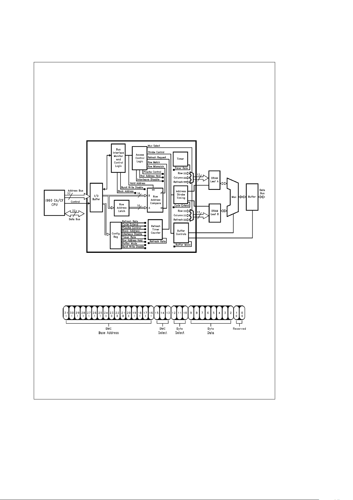
Functional Description
PRODUCT OVERVIEW
The NSBMC960 couples the i960 CA/CF interface to
DRAM access protocols, generates bus buffer and data
multiplexor controls and incorporates system and bus monitor timing resources. These functional elements are shown
in
Figure 1
. A maximum of 8 controllers may be included in a
system, each managing up to 4 banks of memory.
The NSBMC960 directly drives an array of fast page mode
DRAMs. This array may be organized as 1 or 2 leaves of
32 bits each. Standard memory sizes from 256 kbit to
64 Mbit are supported and 8-, 16-, and 32-bit access are
allowed. If interleaved mode is selected, burst access is
zero-wait-state; if memory is non-interleaved, 1-wait-state
burst access results.
The NSBMC960 allows for flexibility in the control of data
buffers to the memory array. Propagation delay is minimized
by providing these controls directly, and design flexibility
maximized by allowing the control strategy to be programmable. Buffers as diverse as 74FCT245, 74FCT543,
74FCT646, 74FCT853 and 74FCT861 may be used without
additional glue logic.
TL/V/11805– 4
FIGURE 1. Functional Block Diagram
CONFIGURATION AND CONTROL
The NSBMC960 contains 64 bits of configuration data that
controls it’s operational mode. The configuration is programmed by sending data on the address bus.
Figure 2
shows the format of a configuration access. The byte select
field determines which byte of the 64-bit field will be updat-
ed by the contents of the byte data field. Bits[1,0]are reserved and must be ‘‘0’’. The base address is fixed at
0xff0f0000 while the BMC select field must match the value
programmed at the ID[2..0]pins. In order to protect against
accidental programming, the configuration registers can
only be modified when the processor is in supervisor mode.
TL/V/11805– 5
FIGURE 2. Address Bus Fields Used to Access Configuration Data
6
Page 7

Functional Description (Continued)
BLOCK ADDRESS FIELD
Once configured, a NSBMC096 responds to access requests within the programmed block address range. The
programmed value sets the starting address of the block,
while the size of the block is determined by the DRAM size
control bits. The block address, however, is constrained to
start on a boundary that is an integer multiple of the block
size. For example, if 1 Mbit
c
1 DRAMs are used, the memory block size is 8 Mbytes and must start on an 8 Mbyte
boundary.
TL/V/11805– 6
FIGURE 3. Configuration Register Control Fields
CYCLE EXTEND
In order to maximize the choice of memory device speeds
that may be used for various system clock rates, the Row
Address Strobe (RAS) period for a basic access may be
programmed for either 3 or 4 clock cycles. When cleared to
‘‘0’’, configuration bit 20 indicates that 3 clock cycles (2 wait
states) are to be used (2-0-0-0 burst access), when set to
‘‘1’’, 4 are required (3 wait states for a basic access 3-0-1-0
for burst). Setting bit 20 to ‘‘1’’ also has the effect of increasing the RAS pre-charge time by 1 clock cycle. Calculation of the number of cycles required per access type is
detailed in the NSBMC096 Application Guide.
BURST WRITE DISABLE
It bit 19 of the configuration word is set to ‘‘1’’, burst write
cycles are disabled. Subsequently, when the NSBMC096
detects the start of a burst write access, it asserts the
BTERM signal to request that the processor terminate the
burst in progress and transfer the remaining data using a
series of simple cycles. This feature is included in order to
facilitate the implementation of systems without latching
buffers. Latching buffers are required to prevent data hold
violations during burst writes. If burst writes are disabled,
latching buffers are no longer required.
ROW ADDRESS HOLD
Bit 18 of the configuration register controls the time at which
the memory address switches from row to column address.
This allows the designer to control the address hold time
relative to RAS so that the slowest memory can be used for
a range of clock speeds. Setting Bit 18 yields the maximum
row address hold time, clearing it shortens the row address
hold in favor of additional column address setup.
INTERLEAVE DISABLE
In cost sensitive applications, it is sometimes desirable for a
system to operate with a single bank of memory so as to
reduce the minimum memory required. In this case the interleave mode bit is programmed to ‘‘1’’. If a second bank of
memory is added, this bit can be programmed to ‘‘0’’ to
enable interleave operation and peak performance. In noninterleave mode a burst access is either 2-1-1-1 with Cycle
Extend disabled, or 3-2-2-2 with Extended Cycle. Non-interleave operation uses only leaf A signals.
7
Page 8

Functional Description (Continued)
BUFFER CONTROL MODE FIELD
The transfer of Data from the memory sub-system to the
i960 bus occurs through buffers controlled by the
NSBMC096. Two of the signals (LEA, LEB) provide transparent latch controls for use during write cycles. LEA and
LEB have variable timing but fixed interpretation. The other
two signals, TXA and TXB, change in both timing and function according to programmed mode. Table II presents
these signals using names that are based on the function
performed.
Signals containing TX are transmit controls for buffers that
have output enables (transmit from the memory system).
Buffers such as ’245s or ’646s, which have direction and
enable pins, are controlled by CE (chip enable) in modes 1
and 3. Signals ending with A or B are specific to one or the
other of the two leaves of memory controlled by the
NSBMC096. Signals without suffixes apply to both leaves.
The signal LeafB/*A, required in some configurations, indicates which memory leaf will be selected on the next clock
cycle.
TABLE II. Interpretation of the Buffer Control
Signals for Various Control Modes
Mode Signal 1 Signal 2
0 TXA TXB
1 CEA CEB
2 TX LeafB/*A
3 CE LeafB/*A
Table III presents some of the possible configurations with
the corresponding mode settings. For a comprehensive discussion of the selection of a buffer strategy, refer to the
NSBMC096 Application Guide.
TABLE III. Possible NSBMC096
Memory/Buffer Configurations
Buffer DRAM Write Read Buffer
Type Type Access Access Mode
74FCT245 Nibble 2-4-4-4* 2-0-0-0 Mode 3
74FCT245 Bit 2-4-4-4* 2-0-0-0 Mode 1
74FCT646 Nibble 1-0-0-0 2-0-0-0 Mode 3
74FCT543 Bit 1-0-0-0 2-0-0-0 Mode 0
Am29C983 Bit 1-0-0-0 2-0-0-0 Mode 2
None Nibble 2-4-4-4* 2-0-0-0 Mode 2, 3
*These configurations have burst writes disabled.
DRAM SIZE FIELD
This three bit field, bits 12 – 14, selects the DRAM device
address size, and consequently, memory block size. Note
that the memory in both leaves of a bank are required to be
of the same size and organization for correct operation. Table IV lists the size codes and the corresponding device
sizes.
TABLE IV. Size Code Settings, DRAM
Density and Address Range Size
Memory Memory Max Memory
Size Code Block Size Banks Types
000 2MB 1 256kx1
001 8MB 1 1MBx1
010 32MB 1 4MBx1
011 128MB 1 16MBx1
100 2MB 4* 64kx4
101 8MB 4* 256k x 4
1 1 0 32 MB 4* 1MBx4
1 1 1 128 MB 4* 4MBx4
*Note that banks are sequentially addressed within a block.
REFRESH RATE FIELD
The system clock frequency is used to derive the period of
DRAM refresh cycles. The refresh rate is calculated as
(PCLK clock frequency) / (16 x (programmed value
a
1)).
If, for example, the system clock is 25 MHz and the programmed value is 24 (0x18), the NSBMC096 will execute
the 256 refresh cycles for a 256k DRAM in 4.096 ms.
The algorithm employed by the NSBMC096 guarantees the
time for complete device refresh, however, individual row
refresh may be delayed so as not to pre-empt bursts in
progress. Since the maximum burst is 6 clock cycles in
length, this delay in no way endangers data integrity. Access to devices other than NSBMC096 controlled memory
are not delayed by refresh, access to memory while refresh
is in progress are completed once the refresh cycle is complete.
TIMER CONTROL FIELD
The 24-bit timer is a counter which scales PCLK by a programmable amount and automatically reloads when terminal count is reached. The contents of the timer cannot be
read directly, however, the counter will generate an interrupt
when terminal count is reached. The timer is disabled following a RESET and the Timer Reload value (Configuration
Bytes 4–6) must be programmed before the timer is enabled.
The terminal count interrupt can be generated to comply
with either edge triggered or level sense interrupt controllers. Edge triggered mode generates a pulse that is low for
two cycles when terminal count is reached. In Level sense
mode, the output is asserted low when terminal count is
reached and the output remains low until the Acknowledge
Timer Interrupt op-code is written to configuration byte 0.
See the section on Operation Control for further detail concerning timer interrupt control.
BUS WATCH TIMER CONTROL FIELD
The NSBMC096 contains circuitry that monitors all bus access requests regardless of the target address. Access
made to a region configured for external ready can hang the
processor if for some reason READY is not returned to terminate the access. The NSBMC096 can detect such a condition and if the bus watch feature is enabled, will return
READY and BERR.
8
Page 9

Functional Description (Continued)
The bus monitor operates by monitoring the state of the
DEN signal. Should it be asserted for longer than the programmed Bus Time Out value in configuration register 7,
Ready is asserted if configuration bit 63 is set. If configuration bit 62 is set, BERR is also asserted. The BERR signal
behaves much like the timer interrupt in that it can be programmed to produce a pulse or a level state.
If level state operation is selected, (configuration bit 61
e
1), BERR will only be deasserted when configuration register 7 is accessed in a read cycle. If configuration bit 61 is
cleared to zero, a two cycle pulse is produced on time-out.
By providing both modes of operation, the BERR signal may
be connected directly to the processor, or to an external
WATCHDOG
TM
circuit.
OPERATION CONTROL FIELD
Byte 0 of the configuration register contains three fields.
The first field (from LSB) is reserved for test purposes and
must be zero for proper in-circuit operation. The second
field is the operation control field which is used to control
the state of the page cache, timer, interrupts and bus error
signal. The third field is the Iow two bits of the refresh rate.
The NSBMC096 has been designed such that if any of the
bits in the operation control field is written with a ‘‘1’’, access to the other two fields is disabled and the previous
value is retained. If all bits in the operation control field are
‘‘0’’, the reserved and refresh rate fields are updated from
the current input.
Since the control register is accessed as a byte, automatic
masking of the non-control field bits simplifies programming
of the control parameters. AII parameters in this field may
be modified on-the-fly, and all functions are disabled by reset. The operational controls have been encoded such that
any access to the register will only modify one parameter.
Bit Control
7 65432 1 0 Function
DD0000DDUpdate Bits 0, 1, 6 and 7 with data D
XX0100XXInstruction Access Page Cache Disable
(Default)
XX0110XXInstruction Access Page Cache Enable
XX0101XXData Access Page Cache Disable (Default)
XX0111XXData Access Page Cache Enable
XX1000XXAcknowledge Timer Interrupt
XX1010XXEnable Timer Output for Level Sense
Interrupt
XX1100XXDisable All Timer Interrupts
XX1110XXEnable Timer Output for Edge Sense
Interrupt
PAGE CACHE MANAGEMENT
The Page Cache management implemented by the
NSBMC096 incorporates a mechanism whereby advantage
can be taken of the page access mode of DRAMs, not only
for burst access, but also for non-sequential data and instruction access. The mechanism relies on the fact that as
long as RAS is asserted, access to the selected row can be
gained by simply asserting a column address and the CAS
strobe. The resulting access is slower than a burst only by
the amount of time required to ensure that the desired address is in the same row as was previously selected.
The benefits of this type of access are obvious, however,
there can be drawbacks. If the required address does not
reside in the same page as that selected, the currently selected row must be released and the new row selected before the access can proceed. The process of de-selecting a
row and selecting a new one requires that the RAS precharge time be allowed to expire before the selection of a
new row can begin. This pre-charge time can require up to
two additional cycles over a standard access startup.
The efficiency of this type of cache (PCache) is related to a
large extent on the locality of reference of the datum being
accessed. For systems that have mixed Instruction and
Data memory systems, PCache efficiency is very dependent
on the behavior of the program being executed as related to
the ‘‘run-length’’ of data and instruction access, the processor internal cache utilization, and the locality of data and
instruction references. Since throughput is lowered by
cache misses, the page cache can be dynamically enabled/
disabled for instruction and/or data access. In this manner
the programmer can apply the mechanism judiciously in order to maximize throughput.
For systems in which Instruction and data spaces are controlled by independent NSBMC096s, the page cache management can be used to greater effect as data and instruction ‘‘run length’’ ceases to be a factor in determining performance. In this type of configuration cache efficiency is
simply a function of locality of reference and a control strategy for the page cache mechanism is much simpler to derive and implement. PCache management is independently
controlled for instruction and data access. A recommended
starting strategy for improving performance of mixed instruction/data systems is to rely on the burst mechanism
and the internal cache for instruction fetching, and enable
PCache for Data access only. This general rule of thumb
can be improved on, once program behavior is benchmarked.
9
Page 10

Application Example
System Clock: 25 MHz
Refresh Rate: 16 ms per row (0c18)
Memory Size: 1 MB x 1 (Sizee1)
Buffer Mode: Signal 1eCEA, Signal 2eCEB
(Mode 1)
Interleave: Enabled
Row Address Hold: (/2 clock cycle
(Row Address Hold
e
0)
Cycle Extend: Disabled (3 clock RAS derived from
t
RSHL
of NSBMC096, RAS access time
of DRAM, buffer delay of 74FCT245
and setup time of the processor’s data
inputs)
Burst Write: Disabled
Base Address: 8 MB (0b000000000100)
Required Configuration for startup
0000 0000 1000 1000 1001 0110 0000 0000 (0x00889600)
Configuration Setup
0xFF0F0000 (0xFF0F0000, 0); /* Config. bits 7..0
e
0 */
0xFF0F0658 (0xFF0F0400
a
(0x96m2), 0); /* Config. bits 15..8e0 */
0xFF0F0A20 (0xFF0F0800
a
(0x88m2), 0); /* Config. bits 23..16e0 */
0xFF0F0C00 (0xFF0F0C00, 0); /* Config. bits 31..24
e
0 */
The ease with which the NSBMC096 may be integrated into
a system design is illustrated in the diagram in
Figure 4
. The
system shown supports an i960 CA/CF with between 2 and
128 MB of memory, depending on the devices selected,
managed by a single NSBMC096. This specific example accommodates 1 MB x 1, 4 MBx1or16MBx1devices.
Connection of the NSBMC096 to the i960 CA/CF processor
is accomplished simply by wiring together pins with the
same names. The only exceptions are READY and BTERM.
If the NSBMC096 is the only device that generates these
two signals, they can be connected directly to the appropri-
ate inputs of the processor and require only a small pull up
resistor to keep them de-asserted when in the high impedance state.
If multiple processor peripherals are connected to READY
or BTERM, 3-state drivers should be used in such a manner
that the signals are actively de-asserted prior to the driver
being placed in its’ high impedance state. If this rule is followed, a simple ‘‘wire or’’ can be used. Alternately, all
sources of READY or BTERM can be combined using multiple input gates and the processor signals driven by the outputs.
TL/V/11805– 7
FIGURE 4. Possible System Interconnection using V96BMC
(Mode 1 where TXA is used as CEA and TXB as CEB)
10
Page 11

Timing Parameters
INTERFACE TIMING
The NSBMC096 interface to the i960 CA/CF has been designed for direct interconnect. It is not necessary to place
other Iogic devices between the processor and the
NSBMC096, nor is their use encouraged. The introduction
of intermediate address or control signal buffers can result
in skews or delays that will require the system clock frequency to be derated for operation under worst case conditions. The timing diagrams presented in this section assume
that all signals between the processor and the NSBMC096
are un-buffered.
REFRESH TIMING
Figure 5
details the timing of the RAS only refresh performed by the memory controller when there is a competing
request from a bus master. A competing request is defined
as any request that occurs between T0 and T5. For any
request in this range, the timing is exactly as shown. As
illustrated, the diagram represents the timing that results
when Cycle Extend is disabled. If Cycle Extend is enabled,
an additional cycle is inserted at T3 and T8.
SIMPLE ACCESS TIMING
The NSBMC096 can return data to the processor in only 3
or 4 clock cycles for a basic access (2 or 3 wait states)
depending on whether Cycle Extend is enabled. If multiple
access cycles are requested back to back then the BMC will
pause for a minimum of 2 clocks between RAS cycles to
insure that the RAS pre-charge time is met. This will result in
5 or 6 clocks between successive simple cycles.
Figure 6
shows the timing relationship between the system
clock, processor control signals and NSBMC096 outputs.
AIl NSBMC096 outputs are derived synchronously with the
exception of t
ARA
(processor address to row address delay). Two simple access cycles are shown in the diagram.
The first is a read cycle that assumes that the NSBMC096
was idle prior to the start of the cycle, the second is backed
onto the first to show the effect of RAS pre-charge imposed
by NSBMC096. If Cycle Extend is enabled, a wait state will
be inserted after cycles T3 and T8.
BURST ACCESS TIMING
When a burst access is requested by the processor, the
NSBMC096 generates the sequence in Figure 7. If the burst
is for 2 words (load double for example), the processor generates *BLAST in T5 and the sequence is shortened appropriately. The first access of the burst sequence begins in the
same manner as a simple access. Consequently the timing
parameters from
Figure 6
may be applied in
Figure 7
.
TL/V/11805– 8
FIGURE 5. Refresh Timing
11
Page 12

Timing Parameters (Continued)
TL/V/11805– 9
FIGURE 6. Basic Access Timing
TL/V/11805– 10
FIGURE 7. Burst Access Timing
12
Page 13

Timing Parameters (Continued)
TL/V/11805– 11
FIGURE 8. Burst Access w/t PCache Hit
Figures 8
and9show the sequence of events that can oc-
cur when PCache is enabled. The sequence in
Figure 8
shows two back-to-back bursts in the same page. This type
of sequence yields the highest data transfer rate achievable
with DRAM.
Figure 9
shows the worst case scenario. This
example shows two back-to-back simple access to different
rows with PCache is enabled.
TL/V/11805– 12
FIGURE 9. Simple Access w/t PCache Miss
13
Page 14

Absolute Maximum Ratings
If Military/Aerospace specified devices are required,
please contact the National Semiconductor Sales
Office/Distributors for availability and specifications.
Supply Voltage (V
CC
)
b
0.3V toa7V
Input Voltage (V
IN
)
b
0.3V to V
CC
a
0.3V
D.C. Input Current (I
IN
)
g
50 mA
Storage Temperature (
O
STG
)
b
65§Ctoa150§C
All Voltages References to Ground
Recommended Operating
Conditions
Supply Voltage (VCC) 4.5V to 5.5V
Ambient Temperature Range (
O
A
)
Plastic Package
b
0§Ctoa70§C
Ceramic Package
b
55§Ctoa85§C
DC Electrical Characteristics
Symbol Description Conditions Min Max Units
V
IL
Low Level Input Voltage V
CC
e
4.75V 1.4 V
V
IH
High Level Input Voltage V
CC
e
5.25V 3.7 V
I
IL
Low Level Input Current V
IN
e
VSS,V
CC
e
5.25V
b
10 mA
I
IH
High Level Input Current V
IN
e
V
CC
e
5.25V 10 mA
V
OL
Low Level Output Voltage V
IN
e
VILor V
IH
0.4 V
I
OL
e
24 mA
V
OH
High Level Output Voltage V
IN
e
VILor V
IH
3.7 V
I
OL
e
24 mA
I
OZL
Low Level TRI-STATE
É
V
IN
e
VILor V
IH
b
20 mA
Output Current V
O
e
V
SS
I
OZH
Low Level TRI-STATE V
IN
e
VILor V
IH
20 mA
Output Current V
O
e
5.25V
I
CC(Max)
Maximum Supply Current Continuous Simple Access 100
mA
Continuous Burst Access 30
C
IN
Input Capacitance 20 pF
C
OUT
Output Capacitance 20 pF
14
Page 15

AC Timing Parameters (Unless otherwise stated V
CC
e
5.0Vg5%, 0§CkT
A
k
70§C.)
Symbol Description
16 MHz 25 MHz 33 MHz
Units
Min Max Min Max Min Max
1. t
ADSU
Address Strobe Setup Time 14 12 9 ns
2. t
ADH
Address Strobe Hold Time 3 3 3 ns
3. t
SU
Synchronous Input Setup 14 12 9 ns
4. t
H
Synchronous Input Hold 3 3 3 ns
5. t
BLSU
BLAST Input Setup 14 12 9 ns
6. t
BLH
BLAST Input Hold 3 3 3 ns
7. t
RZH
READY 3-state to Valid Delay Relative to *PCLK 29 24 19 ns
8. t
RHL
READY Synchronous Assertion Delay 26 21 17 ns
9. t
RLH
READY Synchronous De-assertion Delay 25 20 16 ns
10. t
RHZ
READY Valid to 3-state Delay Relative to *PCLK 27 22 17 ns
11. t
ARA
Address Input to Row Address Output Delay (Note 1) 23 19 15 ns
12. t
RAH
*PCLK or PCLK to Row Address Hold 40 33 26 ns
13. t
CAV
*PCLK or PCLK to Column Address Valid (Note 1) 38 31 25 ns
14. t
CAH
PCLK to Column Address Hold 4 4 4 ns
15. t
DRAH
DRAM Row Address Hold (Note 2) t
M-4
t
M-4
t
M-3
ns
16. t
RSHL
PCLK to RAS Asserted Delay (Note 1) 29 24 19 ns
17. t
RSLH
PCLK to RAS De-asserted Delay (Note 1) 26 21 17 ns
18. t
CHL
PCLK to CAS Asserted Delay (Note 1) 23 19 15 ns
19. t
CLH
PCLK to CAS De-asserted Delay (Note 1) 20 16 13 ns
20. t
BHL
PCLK to Buffer Control Asserted Delay (Note 1) 26 21 17 ns
21. t
BLH
PCLK to Buffer Control De-asserted Delay (Note 1) 4 23 4 19 4 15 ns
22. t
BSV
PCLK to Bank Select Valid Time (Note 1) 26 21 17 ns
23. t
BSH
PCLK to Bank Select Hold Time (Note 1) 4 4 4 ns
24. t
WEHL
*PCLK to Write Enable Asserted Delay (Note 1) 31 25 20 ns
25. t
WELH
PCLK to Write Enable De-asserted Delay (Note 1) ns
26. t
BCAH
*PCLK to Column Address Hold Time (Burst) (Note 1) 5 5 4 ns
27. t
BCAV
*PCLK to Column Address Valid Delay (Burst) (Note 1) 29 23 19 ns
28. t
LEHL
*PCLK to Latch Enable Assertion 23 19 15 ns
29. t
LELH
PCLK to Latch Enable De-assertion 20 16 13 ns
30. t
RFA
PCLK to Row Address Valid (Refresh) 38 31 25 ns
31. t
RFH
PCLK to Row Address Hold (Refresh) 5 5 4 ns
32. t
RFHL
REFRESH Synchronous Assertion Delay 20 16 13 ns
33. t
RFLH
REFRESH Synchronous De-assertion Delay 20 16 13 ns
*Signal output delays are measured relative to PCLK (except as indicated) using a 50 pF load.
Note 1: Derate the given delays by 0.006 ns per pF of load in excess of 50 pF.
Note 2: t
M
e
PCLK High duration when configuration bit 18e0. t
M
e
PCLK cycle timee1/
(PCLK frequency)
for configuration bit 18e1. Timing for Rev AB
silicon.
15
Page 16

Errata for NSBMC096
The document defines all known errata related to the operation of the NSBMC096 Memory Controller.
ERRATUM
Ý
1
Pulse mode interrupts from the NSBMC096 are two cycles
long. The current rev. of the i960CA/CF requires a minimum
interrupt pulse width of three clock cycles.
RECOMMENDED FIX
Program the NSBMC096 for level mode interrupts.
ERRATUM
Ý
2
When the NSBMC096 is programmed for extended timing
mode operation, back to back memory read cycles will fail.
RECOMMENDED FIX
Program the i960CA/CF memory region for the NSBMC096
to insert one wait state following each memory access (i.e.,
Set N
XDA
e
1).
Ordering Code Information
NS BMC 096 VF 33
National Semiconductor Frequency
16 MHz
Mode
25 MHz
Burst Mode Controller
33 MHz
Processor
Packaging
Intel i960
VF 132-Lead PQFP
16
Page 17

17
Page 18

NSBMC096-16/-25/-33 Burst Memory Controller
Physical Dimensions inches (millimeters)
132-Pin Plastic Quad Flatpak (PQFP)
Order Number NSBMC096VF
NS Package Number VF132A
LIFE SUPPORT POLICY
NATIONAL’S PRODUCTS ARE NOT AUTHORIZED FOR USE AS CRITICAL COMPONENTS IN LIFE SUPPORT
DEVICES OR SYSTEMS WITHOUT THE EXPRESS WRITTEN APPROVAL OF THE PRESIDENT OF NATIONAL
SEMICONDUCTOR CORPORATION. As used herein:
1. Life support devices or systems are devices or 2. A critical component is any component of a life
systems which, (a) are intended for surgical implant support device or system whose failure to perform can
into the body, or (b) support or sustain life, and whose be reasonably expected to cause the failure of the life
failure to perform, when properly used in accordance support device or system, or to affect its safety or
with instructions for use provided in the labeling, can effectiveness.
be reasonably expected to result in a significant injury
to the user.
National Semiconductor National Semiconductor National Semiconductor National Semiconductor
Corporation Europe Hong Kong Ltd. Japan Ltd.
1111 West Bardin Road Fax: (
a
49) 0-180-530 85 86 13th Floor, Straight Block, Tel: 81-043-299-2309
Arlington, TX 76017 Email: cnjwge@tevm2.nsc.com Ocean Centre, 5 Canton Rd. Fax: 81-043-299-2408
Tel: 1(800) 272-9959 Deutsch Tel: (
a
49) 0-180-530 85 85 Tsimshatsui, Kowloon
Fax: 1(800) 737-7018 English Tel: (
a
49) 0-180-532 78 32 Hong Kong
Fran3ais Tel: (
a
49) 0-180-532 93 58 Tel: (852) 2737-1600
Italiano Tel: (
a
49) 0-180-534 16 80 Fax: (852) 2736-9960
National does not assume any responsibility for use of any circuitry described, no circuit patent licenses are implied and National reserves the right at any time without notice to change said circuitry and specifications.
 Loading...