

Page 1
TL/EE11331
NS32FX100-15/NS32FX100-20/NS32FV100-20/NS32FV100-25/
NS32FX200-20/NS32FX200-25 System Controller
PRELIMINARY
July 1992
NS32FX100-15/NS32FX100-20/NS32FV100-20/
NS32FV100-25/NS32FX200-20/NS32FX200-25
System Controller
General Description
The NS32FX200, NS32FV100 and NS32FX100 are highly
integrated system chips designed for a FAX system based
on National Semiconductor’s embedded processorsÐ
NS32FX161, NS32FV16 or NS32FX164. The NS32FX100 is
the common core for all three system chips. The
NS32FV100 and NS32FX200 offer additional functions.
Throughout this document, references to the NS32FX100
also apply to both the NS32FV100 and the NS32FX200.
Specific NS32FV100 or NS32FX200 features are explicitly
indicated.
The NS32FX200, NS32FV100 and NS32FX100 feature an
interface to devices like stepper motors, printers and scanners, a Sigma-Delta CODEC, an elapsed-time counter, a
DMA controller, an interrupt controller, and a UART.
The NS32FX200 is optimized for high-end FAX applications,
such as plain-paper FAX and multifunctional peripherals.
The NS32FX100, is optimized for low-cost FAX applications. The NS32FV100 is optimized for thermal paper FAX
machines with Digital Answering Machine support.
Features
Y
Direct interface to the NS32FX161, NS32FV16 and
NS32FX164 embedded processors
Y
Supports a variety of Contact Image Sensor (CIS) and
Charge Coupled Device (CCD) scanners
Y
Direct interface to a variety of Thermal Print Head
(TPH) printers. Bitmap shifter and DMA channels facilitate the connection of other types of printers
Y
Supports two stepper motors
Y
Direct interface to ROM and SRAM. The NS32FX200
and NS32FV100, in addition, interface to DRAM
devices
Y
Programmable wait state generator
Y
Demultiplexed address and data buses
Y
Multiplexed DRAM address bus (NS32FX200 and
NS32FV100)
Y
Supports 3V freeze mode by maintaining only elapsed
time counter
Y
Control of power consumption by disabling inactive
modules and reducing the clock frequency
Y
Operating frequency
Ð Normal mode: 19.6608 MHzÐ24.576 MHz in steps
of 1.2288 MHz. (NS32FX200)
Ð Normal mode: 19.6608 MHzÐ24.576 MHz in steps
of 1.2288 MHz. (NS32FV100)
Ð Normal mode: 14.7456 MHzÐ19.6608 MHz in steps
of 1.2288 MHz. (NS32FX100)
Ð Power Save mode: Normal mode frequency divided
by sixteen
Y
On-Chip full duplex Sigma-Delta CODEC with:
Ð Total harmonic distortion better than
b
70 dB
Ð Programmable hybrid balance filter
Ð Programmable reception and transmission filters
Ð Programmable gain control
Y
On-Chip Interrupt Control Unit with:
Ð 16 interrupt sources
Ð Programmable triggering mode
Y
On-Chip counters, WATCHDOGTM, UART,
MICROWIRE
TM
, System Clock Generator, and I/O
ports
Y
On-Chip DMA controller (NS32FX200Ðfour channels,
NS32FX100, NS32FV100Ðthree channels)
Y
Up to 37 on-chip general purpose I/O pins, expandable
externally
Y
Flexible allocation of I/O and modules’ pins
Y
132-pin JEDEC PQFP package
TL/EE/11331– 1
FIGURE 1-1. A FAX Controller Block Diagram
TRI-STATEÉis a registered trademark of National Semiconductor Corporation.
MICROWIRE
TM
and WATCHDOGTMare trademarks of National Semiconductor Corporation.
C
1995 National Semiconductor Corporation RRD-B30M105/Printed in U. S. A.
Page 2

Table of Contents
1.0 FAX SYSTEM CONFIGURATION АААААААААААААААААА6
1.1 Block Diagram Description АААААААААААААААААААААА6
1.2 Module Diagram ААААААААААААААААААААААААААААААА7
1.2.1 Bus and Memory Controller (BMC) АААААААААА8
1.2.2 Timing Control Unit (TCU) ААААААААААААААААА8
1.2.3 Sigma-Delta CODEC (SDC) АААААААААААААААА8
1.2.4 Scanner Controller (SCANC) ААААААААААААААА8
1.2.5 Printer Controller (PRNTC) ААААААААААААААААА8
1.2.6 DMA Controller (DMAC) ААААААААААААААААААА8
1.2.7 Universal Asynchronous Receiver-Transmitter
(UART)АААААААААААААААААААААААААААААААААА8
1.2.8 MICROWIRE (MWIRE) АААААААААААААААААААА8
1.2.9 Interrupt Control Unit (ICU)ААААААААААААААААА8
1.2.10 Ports АААААААААААААААААААААААААААААААААА8
1.3 Operation Modes АААААААААААААААААААААААААААААА8
1.3.1 Functionality ААААААААААААААААААААААААААААА9
2.0 ARCHITECTURE ААААААААААААААААААААААААААААААА10
2.1 MCFGРModule Configuration Register АААААААААА10
2.2 Timing Control Unit (TCU) АААААААААААААААААААААА10
2.2.1 Features ААААААААААААААААААААААААААААААА10
2.2.2 Operation АААААААААААААААААААААААААААААА10
2.2.2.1 External Clocks АААААААААААААААААА11
2.2.2.2 Internal Clocks ААААААААААААААААААА11
2.2.3 Registers ААААААААААААААААААААААААААААААА12
2.2.3.1 Usage Recommendations ААААААААА13
2.3 Sigma-Delta CODEC (SDC) АААААААААААААААААААА13
2.3.1 Features ААААААААААААААААААААААААААААААА13
2.3.2 Operation АААААААААААААААААААААААААААААА13
2.3.2.1 Block Diagram ААААААААААААААААААА13
2.3.2.2 On-Chip Digital Blocks АААААААААААА15
2.3.3 Programmable Functions ААААААААААААААААА15
2.3.3.1 Sigma-Delta ON/OFFААААААААААААА15
2.3.4 Off-Chip Analog Circuits АААААААААААААААААА15
2.3.4.1 Analog Transmitter ААААААААААААААА17
2.3.4.2 Analog Receiver ААААААААААААААААА17
2.3.5 Registers ААААААААААААААААААААААААААААААА17
2.3.6 Usage Recommendations АААААААААААААААА18
2.4 Scanner Controller (SCANC) ААААААААААААААААААА18
2.4.1 Features ААААААААААААААААААААААААААААААА18
2.4.2 Operation АААААААААААААААААААААААААААААА18
2.4.2.1 Scanner Signals Generator Block ÀÀ19
2.4.2.2 Scanner Period Pulse (SPP)
Generation АААААААААААААААААААААА20
2.4.2.3 Video Handling Block ААААААААААААА21
2.4.2.4 Threshold DAC (Dithering and
Automatic Background Control) ÀÀÀÀ22
2.4.2.5 Stepper Motor Control Block ААААААА23
2.0 ARCHITECTURE (Continued)
2.4.3 Registers ААААААААААААААААААААААААААААААААА23
2.4.4 Usage Recommendations АААААААААААААААААА24
2.5 Printer Controller (PRNTC) ААААААААААААААААААААА25
2.5.1 Features ААААААААААААААААААААААААААААААА25
2.5.2 Operation АААААААААААААААААААААААААААААА25
2.5.2.1 Printer Bitmap Shifter BlockАААААААА25
2.5.2.2 Thermal Print-Head Control Block ÀÀ25
2.5.3 Registers ААААААААААААААААААААААААААААААА28
2.5.4 Usage Recommendations АААААААААААААААА28
2.6 Direct Memory Access Controller (DMAC) АААААААА29
2.6.1 Features ААААААААААААААААААААААААААААААА29
2.6.2 Description ААААААААААААААААААААААААААААА29
2.6.2.1 A General DMA Channel АААААААААА29
2.6.2.2 Transfer TypesААААААААААААААААААА29
2.6.2.3 Operation Modes ААААААААААААААААА29
2.6.3 Detailed Operation Flow АААААААААААААААААА29
2.6.4 NS32FX200 DMA Channels АААААААААААААА30
2.6.5 Registers ААААААААААААААААААААААААААААААА30
2.6.6 Usage Recommendations АААААААААААААААА32
2.6.7 DMAC Bus Cycles ААААААААААААААААААААААА32
2.7 Universal Asynchronous Receiver-Transmitter
(UART) АААААААААААААААААААААААААААААААААААААА36
2.7.1 Features ААААААААААААААААААААААААААААААА36
2.7.2 Operation АААААААААААААААААААААААААААААА36
2.7.3 Registers ААААААААААААААААААААААААААААААА37
2.7.4 Usage Recommendations АААААААААААААААА38
2.8 MICROWIRE (MWIRE) АААААААААААААААААААААААА38
2.8.1 Features ААААААААААААААААААААААААААААААА38
2.8.2 Operation АААААААААААААААААААААААААААААА38
2.8.3 Registers ААААААААААААААААААААААААААААААА38
2.8.4 Usage Recommendations АААААААААААААААА40
2.9 Interrupt Control Unit (ICU) ААААААААААААААААААААА40
2.9.1 Features ААААААААААААААААААААААААААААААА40
2.9.2 Operation АААААААААААААААААААААААААААААА40
2.9.3 Registers ААААААААААААААААААААААААААААААА41
2.9.4 Usage Recommendations АААААААААААААААА41
2.10 Ports Module АААААААААААААААААААААААААААААААА41
2.10.1 Features ААААААААААААААААААААААААААААА41
2.10.2 Operation АААААААААААААААААААААААААААА41
2.10.2.1 General Purpose Input/Output
Ports АААААААААААААААААААААААА41
2.10.2.2 External Output Port Extension À43
2.10.2.3 Stepper Motors Output Ports ÀÀÀ43
2.10.3 Registers АААААААААААААААААААААААААААА43
2.10.4 Usage Recommendations АААААААААААААА45
2
Page 3

Table of Contents (Continued)
2.0 ARCHITECTURE (Continued)
2.11 Bus and Memory Controller (BMC) ААААААААААААА45
2.11.1 Features ААААААААААААААААААААААААААААА45
2.11.2 Operation АААААААААААААААААААААААААААА45
2.11.2.1 Zones 0, 1 (ROM and SRAM)
Transactions ААААААААААААААААА46
2.11.2.2 Zone 2 (Dynamic Memory)
Transactions (NS32FX200 and
NS32FV100 only) ААААААААААААА46
2.11.2.3 Zone 3 (I/O) Transactions ААААА47
2.11.2.4 Operation in Freeze ModeАААААА47
2.11.2.5 On-Chip Registers Access ААААА47
2.11.3 Registers АААААААААААААААААААААААААААА47
2.11.4 Usage Recommendations АААААААААААААА48
2.12 Register Summary ААААААААААААААААААААААААААА48
2.12.1 NS32FX100 Registers Access Method ÀÀÀ48
2.12.2 NS32FX200, NS32FV100 and NS32FX100
Registers АААААААААААААААААААААААААААА48
3.0 SYSTEM INTERFACEААААААААААААААААААААААААААА53
3.1 Power and Grounding ААААААААААААААААААААААААА53
3.2 Clocks and Traps Connectivity АААААААААААААААААА53
3.0 SYSTEM INTERFACE (Continued)
3.3 Control of Power Consumption ААААААААААААААААА53
3.4 Bus Cycles ААААААААААААААААААААААААААААААААААА54
4.0 DEVICE SPECIFICATIONS АААААААААААААААААААААА62
4.1 NS32FX100 Pin Descriptions ААААААААААААААААААА62
4.1.1 Supplies ААААААААААААААААААААААААААААААА62
4.1.2 Input Signals АААААААААААААААААААААААААААА62
4.1.3 Output Signals АААААААААААААААААААААААААА63
4.1.4 Input/Output Signals ААААААААААААААААААААА64
4.2 Output Signal Levels АААААААААААААААААААААААААА64
4.2.1 Freeze Mode Output Signals АААААААААААААА65
4.2.2 Reset/Power Restore Output Signals АААААА65
4.3 Absolute Maximum Ratings АААААААААААААААААААА67
4.4 Electrical Characteristics ААААААААААААААААААААААА67
4.5 Analog Electrical Characteristics АААААААААААААААА69
4.6 Switching Characteristics АААААААААААААААААААААА70
4.6.1 Definitions АААААААААААААААААААААААААААААА70
4.6.2 Timing Tables ААААААААААААААААААААААААААА71
4.6.2.1 Output Signals: Internal Propagation
Delays АААААААААААААААААААААААААА71
4.6.2.2 Input Signal RequirementsААААААААА76
APPENDIX A: CODEC TRANSMISSION
PERFORMANCE ААААААААААААААААААААА92
3
Page 4

List of Figures
FIGURE 1-1 A FAX Controller Block DiagramААААААААААААААААААААААААААААААААААААААААААААААААААААААААААААААААААААА1
FIGURE 1-2 NS32FX100 Module Diagram ААААААААААААААААААААААААААААААААААААААААААААААААААААААААААААААААААААААА7
FIGURE 1-3 NS32FV100 Module Diagram ААААААААААААААААААААААААААААААААААААААААААААААААААААААААААААААААААААААА7
FIGURE 1-4 NS32FX200 Module Diagram ААААААААААААААААААААААААААААААААААААААААААААААААААААААААААААААААААААААА7
FIGURE 1-5 System Chip States and Operation Modes АААААААААААААААААААААААААААААААААААААААААААААААААААААААААААА9
FIGURE 2-1 Clocks and Traps Connectivity ААААААААААААААААААААААААААААААААААААААААААААААААААААААААААААААААААААА10
FIGURE 2-2 High Speed Oscillator Clocks АААААААААААААААААААААААААААААААААААААААААААААААААААААААААААААААААААААА11
FIGURE 2-3 Low Speed Oscillator Clocks АААААААААААААААААААААААААААААААААААААААААААААААААААААААААААААААААААААА11
FIGURE 2-4 Sigma-Delta Block Diagram ААААААААААААААААААААААААААААААААААААААААААААААААААААААААААААААААААААААА14
FIGURE 2-5 SDC Off-Chip Analog Circuit ААААААААААААААААААААААААААААААААААААААААААААААААААААААААААААААААААААААА16
FIGURE 2-6 Block Diagram of Scanner’s Signals Generator Block ААААААААААААААААААААААААААААААААААААААААААААААААА19
FIGURE 2-7 Scanner Pixel Control SignalsАААААААААААААААААААААААААААААААААААААААААААААААААААААААААААААААААААААА20
FIGURE 2-8 Scanner Period Control Signals АААААААААААААААААААААААААААААААААААААААААААААААААААААААААААААААААААА21
FIGURE 2-9 Block Diagram of Scanner’s Video Handling BlockАААААААААААААААААААААААААААААААААААААААААААААААААААА21
FIGURE 2-10 Dither Cyclic Buffer ААААААААААААААААААААААААААААААААААААААААААААААААААААААААААААААААААААААААААААААА22
FIGURE 2-11 Bitmap Shifter Signals АААААААААААААААААААААААААААААААААААААААААААААААААААААААААААААААААААААААААААА25
FIGURE 2-12 Four Strobes Mode (STBM
e
00) АААААААААААААААААААААААААААААААААААААААААААААААААААААААААААААААААА26
FIGURE 2-13 Two Strobes Mode (STBMe01) АААААААААААААААААААААААААААААААААААААААААААААААААААААААААААААААААА26
FIGURE 2-14 Temperature ADC АААААААААААААААААААААААААААААААААААААААААААААААААААААААААААААААААААААААААААААААА27
FIGURE 2-15 DMA Fly-By Read Transaction (DIRe0, FBYe0) АААААААААААААААААААААААААААААААААААААААААААААААААААА32
FIGURE 2-16 DMA Fly-By Write Transaction (DIRe1, FBYe0)ААААААААААААААААААААААААААААААААААААААААААААААААААААА33
FIGURE 2-17 DMA Memory to I/O Read Transaction (DIR
e
0, NFBYe1)АААААААААААААААААААААААААААААААААААААААААААА34
FIGURE 2-18 DMA I/O to Memory Write Transaction (DIRe1, NFBYe1) АААААААААААААААААААААААААААААААААААААААААААА35
FIGURE 2-19 Two Adjacent Fly-By DMA TransactionsААААААААААААААААААААААААААААААААААААААААААААААААААААААААААААА36
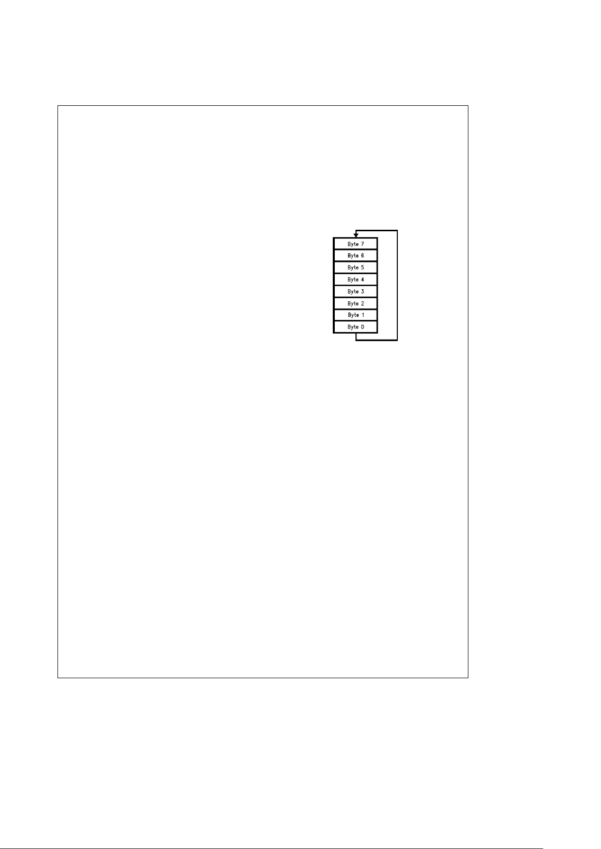
FIGURE 2-20 Character Format АААААААААААААААААААААААААААААААААААААААААААААААААААААААААААААААААААААААААААААААА37
FIGURE 2-21 MICROWIRE Transaction (CLKM
e
0)ААААААААААААААААААААААААААААААААААААААААААААААААААААААААААААААА39
FIGURE 2-22 MICROWIRE Transaction (CLKMe1)ААААААААААААААААААААААААААААААААААААААААААААААААААААААААААААААА39
FIGURE 2-23 Port A АААААААААААААААААААААААААААААААААААААААААААААААААААААААААААААААААААААААААААААААААААААААААА42
FIGURE 2-24 Port B АААААААААААААААААААААААААААААААААААААААААААААААААААААААААААААААААААААААААААААААААААААААААА42
FIGURE 2-25 Port C АААААААААААААААААААААААААААААААААААААААААААААААААААААААААААААААААААААААААААААААААААААААААА42
FIGURE 2-26 External Output Port ExtensionААААААААААААААААААААААААААААААААААААААААААААААААААААААААААААААААААААА43
FIGURE 3-1 Power and Ground ConnectionsАААААААААААААААААААААААААААААААААААААААААААААААААААААААААААААААААААА53
FIGURE 3-2 Oscillator Circuits АААААААААААААААААААААААААААААААААААААААААААААААААААААААААААААААААААААААААААААААА53
FIGURE 3-3 Zones 0, 1 (ROM/SRAM) Read Transaction, Zero Wait State АААААААААААААААААААААААААААААААААААААААААА54
FIGURE 3-4 Zones 0, 1 (ROM/SRAM) Read Transaction, One Wait State АААААААААААААААААААААААААААААААААААААААААА54
FIGURE 3-5 Zones 0, 1 (ROM/SRAM) Write Transaction, Zero Wait State АААААААААААААААААААААААААААААААААААААААААА55
FIGURE 3-6 Zones 0, 1 (ROM/SRAM) Write Transaction, One Wait StateААААААААААААААААААААААААААААААААААААААААААА55
FIGURE 3-7 Zone 2 (DRAM) Refresh Transaction, Zero Wait State АААААААААААААААААААААААААААААААААААААААААААААААА56
FIGURE 3-8 Zone 2 (DRAM) Refresh Transaction, Three Wait States АААААААААААААААААААААААААААААААААААААААААААААА56
FIGURE 3-9 Freeze Mode Refresh Transaction Waveform АААААААААААААААААААААААААААААААААААААААААААААААААААААААА56
FIGURE 3-10 Zone 2 (DRAM) Read Transaction, Zero Wait State ААААААААААААААААААААААААААААААААААААААААААААААААААА57
FIGURE 3-11 Zones 0, 1 Access Delayed by a Refresh Transaction (No Wait) АААААААААААААААААААААААААААААААААААААААА57
FIGURE 3-12 Zone 2 (DRAM) Read Transaction, One Wait State ААААААААААААААААААААААААААААААААААААААААААААААААААА58
FIGURE 3-13 Zone 2 (DRAM) Write Transaction, Zero Wait State ААААААААААААААААААААААААААААААААААААААААААААААААААА58
FIGURE 3-14 Zone 2 (DRAM) Write Transaction, One Wait State ААААААААААААААААААААААААААААААААААААААААААААААААААА59
FIGURE 3-15 Zone 3 (I/O) Read Transaction, Two Wait States ААААААААААААААААААААААААААААААААААААААААААААААААААААА59
FIGURE 3-16 Zone 3 (I/O) Read Transaction, Four Wait StatesААААААААААААААААААААААААААААААААААААААААААААААААААААА60
FIGURE 3-17 Zone 3 (I/O) Write Transaction, Four Wait States ААААААААААААААААААААААААААААААААААААААААААААААААААААА60
FIGURE 3-18 Zone 3 (I/O) Write Transaction, Six Wait States АААААААААААААААААААААААААААААААААААААААААААААААААААААА61
FIGURE 3-19 CPU/DMA ArbitrationААААААААААААААААААААААААААААААААААААААААААААААААААААААААААААААААААААААААААААА61
FIGURE 3-20 Spaced Memory Transaction, Two Tidles after T4 АААААААААААААААААААААААААААААААААААААААААААААААААААА61
4
Page 5

List of Figures (Continued)
FIGURE 4-1 Connection DiagramРTop View ААААААААААААААААААААААААААААААААААААААААААААААААААААААААААААААААААА66
FIGURE 4-2 Analog Circuitry Block Diagram АААААААААААААААААААААААААААААААААААААААААААААААААААААААААААААААААААА69
FIGURE 4-3 TTLРOutput Signals Specification StandardААААААААААААААААААААААААААААААААААААААААААААААААААААААААА70
FIGURE 4-4 TTLРInput Signals Specification Standard АААААААААААААААААААААААААААААААААААААААААААААААААААААААААА70
FIGURE 4-5 CMOSРOutput Signals Specification Standard АААААААААААААААААААААААААААААААААААААААААААААААААААААА70
FIGURE 4-6 CMOSРInput Signals Specification Standard АААААААААААААААААААААААААААААААААААААААААААААААААААААААА70
FIGURE 4-7 Input HysteresisАААААААААААААААААААААААААААААААААААААААААААААААААААААААААААААААААААААААААААААААААА70
FIGURE 4-8 Clock Waveforms АААААААААААААААААААААААААААААААААААААААААААААААААААААААААААААААААААААААААААААААА79
FIGURE 4-9 DRAM Read Bus Cycle ААААААААААААААААААААААААААААААААААААААААААААААААААААААААААААААААААААААААААА79
FIGURE 4-10 DRAM Write Bus Cycle ААААААААААААААААААААААААААААААААААААААААААААААААААААААААААААААААААААААААААА80
FIGURE 4-11 ROM/SRAM Read Bus Cycle АААААААААААААААААААААААААААААААААААААААААААААААААААААААААААААААААААААА81
FIGURE 4-12 ROM/SRAM Write Bus Cycle (One Wait State)ААААААААААААААААААААААААААААААААААААААААААААААААААААААА82
FIGURE 4-13 I/O Read Bus Cycle АААААААААААААААААААААААААААААААААААААААААААААААААААААААААААААААААААААААААААААА83
FIGURE 4-14 I/O Write Bus Cycle АААААААААААААААААААААААААААААААААААААААААААААААААААААААААААААААААААААААААААААА83
FIGURE 4-15 DRAM Refresh Bus Cycles АААААААААААААААААААААААААААААААААААААААААААААААААААААААААААААААААААААААА84
FIGURE 4-16 DMA Read Transaction (DIR
e
0) АААААААААААААААААААААААААААААААААААААААААААААААААААААААААААААААААА85
FIGURE 4-17 DMA Write Transaction (DIR
e
1) АААААААААААААААААААААААААААААААААААААААААААААААААААААААААААААААААА86
FIGURE 4-18 Interrupt Signals Timing ААААААААААААААААААААААААААААААААААААААААААААААААААААААААААААААААААААААААААА87
FIGURE 4-19 Sigma-Delta Signals TimingАААААААААААААААААААААААААААААААААААААААААААААААААААААААААААААААААААААААА87
FIGURE 4-20 SBYPS Input Signal Timing АААААААААААААААААААААААААААААААААААААААААААААААААААААААААААААААААААААААА87
FIGURE 4-21 Printer Signals TimingААААААААААААААААААААААААААААААААААААААААААААААААААААААААААААААААААААААААААААА88
FIGURE 4-22 Reset Signals Timing ААААААААААААААААААААААААААААААААААААААААААААААААААААААААААААААААААААААААААААА88
FIGURE 4-23 Scanner Signals Timing ААААААААААААААААААААААААААААААААААААААААААААААААААААААААААААААААААААААААААА89
FIGURE 4-24 UART Signals Timing ААААААААААААААААААААААААААААААААААААААААААААААААААААААААААААААААААААААААААААА90
FIGURE 4-25 MWIRE Signals TimingАААААААААААААААААААААААААААААААААААААААААААААААААААААААААААААААААААААААААААА90
FIGURE 4-26 Ports Signals Timing АААААААААААААААААААААААААААААААААААААААААААААААААААААААААААААААААААААААААААААА91
FIGURE 4-27 Analog Signals Timing АААААААААААААААААААААААААААААААААААААААААААААААААААААААААААААААААААААААААААА91
List of Tables
TABLE 2-1 CTTL, MCLON and MCLOFF ValuesАААААААААААААААААААААААААААААААААААААААААААААААААААААААААААААААААА12
TABLE 2-2 Component Values ААААААААААААААААААААААААААААААААААААААААААААААААААААААААААААААААААААААААААААААААА15
TABLE 2-3 Interrupt Sources and Priority Levels АААААААААААААААААААААААААААААААААААААААААААААААААААААААААААААААААА40
TABLE 2-4 DRAM Address Multiplexing ААААААААААААААААААААААААААААААААААААААААААААААААААААААААААААААААААААААААА46
TABLE 2-5 DRAM Address Sizes ААААААААААААААААААААААААААААААААААААААААААААААААААААААААААААААААААААААААААААААА46
TABLE 3-1 R, C and L Values АААААААААААААААААААААААААААААААААААААААААААААААААААААААААААААААААААААААААААААААААА53
TABLE 3-2 System Chip Operation Modes and Power ConsumptionААААААААААААААААААААААААААААААААААААААААААААААААА53
TABLE A-1 Transmitter Performance АААААААААААААААААААААААААААААААААААААААААААААААААААААААААААААААААААААААААААА92
TABLE A-2 Receiver Performance АААААААААААААААААААААААААААААААААААААААААААААААААААААААААААААААААААААААААААААА93
5
Page 6

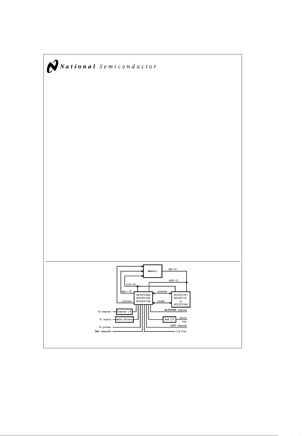
1.0 Fax-System Configuration
A typical FAX system based on the NS32FX100,
NS32FX200 or NS32FV100, is shown in
Figure 1-1
.
1.1 BLOCK DIAGRAM DESCRIPTION
CPU. The typical FAX system shown below is based on a
single embedded processor. The choice between the
NS32FX161, NS32FV16 and the NS32FX164 depends on
the specific application requirements.
System Chip. The FAX-system chip interfaces between
FAX-system peripheral devices, such as motors, printers
and scanners, and the embedded processor. The chip contains FAX-system elements such as CODEC, DMA Controller, Interrupt Control Unit and counters.
Scanner. Either a Charge-Coupled Device (CCD) scanner
or a Contact Image Sensor (CIS) scanner may be used. The
NS32FX100 incorporates most of the video circuits, such as
shading compensation, dithering and digitizing, which are
required for the scanner interface.
Printer. A Thermal Print Head (TPH) can be connected directly to the NS32FX100. Other types of printer engine,
such as laser or ink-jet, can easily be interfaced to the
NS32FX100 via an additional, small ASIC.
Motors. The NS32FX100 controls two stepper motors. The
only external components required to operate the motors
are buffers/drivers.
DAA I/F. The telephone line is accessed via a Data Access
Arrangement (DAA). The NS32FX100 contains the digital
part of a Sigma-Delta CODEC, which connects to the DAA.
A few external components are required to implement the
analog part of the CODEC.
Memory. The NS32FX100 directly controls ROM and
SRAM. Both the NS32FX200 and the NS32FV100 directly
control DRAM, in addition to ROM and SRAM.
Memory access time is also controlled by the NS32FX100,
thus allowing the designer to tune memory price and system
performance.
MICROWIRE. The serial channel, with programmable interface parameters, can be used by advanced FAX systems to
interface with other devices (such as EEPROMs).
UART. This serial channel, with programmable interface parameters, can be used by advanced fax systems to communicate with other devices (e.g., host machines).
I/O Pins. General purpose I/O pins are used both to monitor (e.g., ring detector read) and control (e.g. scanner light
control) the FAX-system peripheral devices.
DMA Channels:
NS32FX100 and NS32FV100. The NS32FX100 and
NS32FV100 have three DMA channels which are used to
interface the scanner and the printer. All three channels
may be allocated for external usage (e.g., Centronics parallel interface, Ethernet).
NS32FX200. The NS32FX200 has four DMA channels.
Three channels are used by the NS32FX200 to interface to
the scanner and the printer, and one channel is for external
usage. All four channels may be allocated for external usage (e.g., Centronics parallel interface, Ethernet).
6
Page 7
1.0 Fax-System Configuration (Continued)
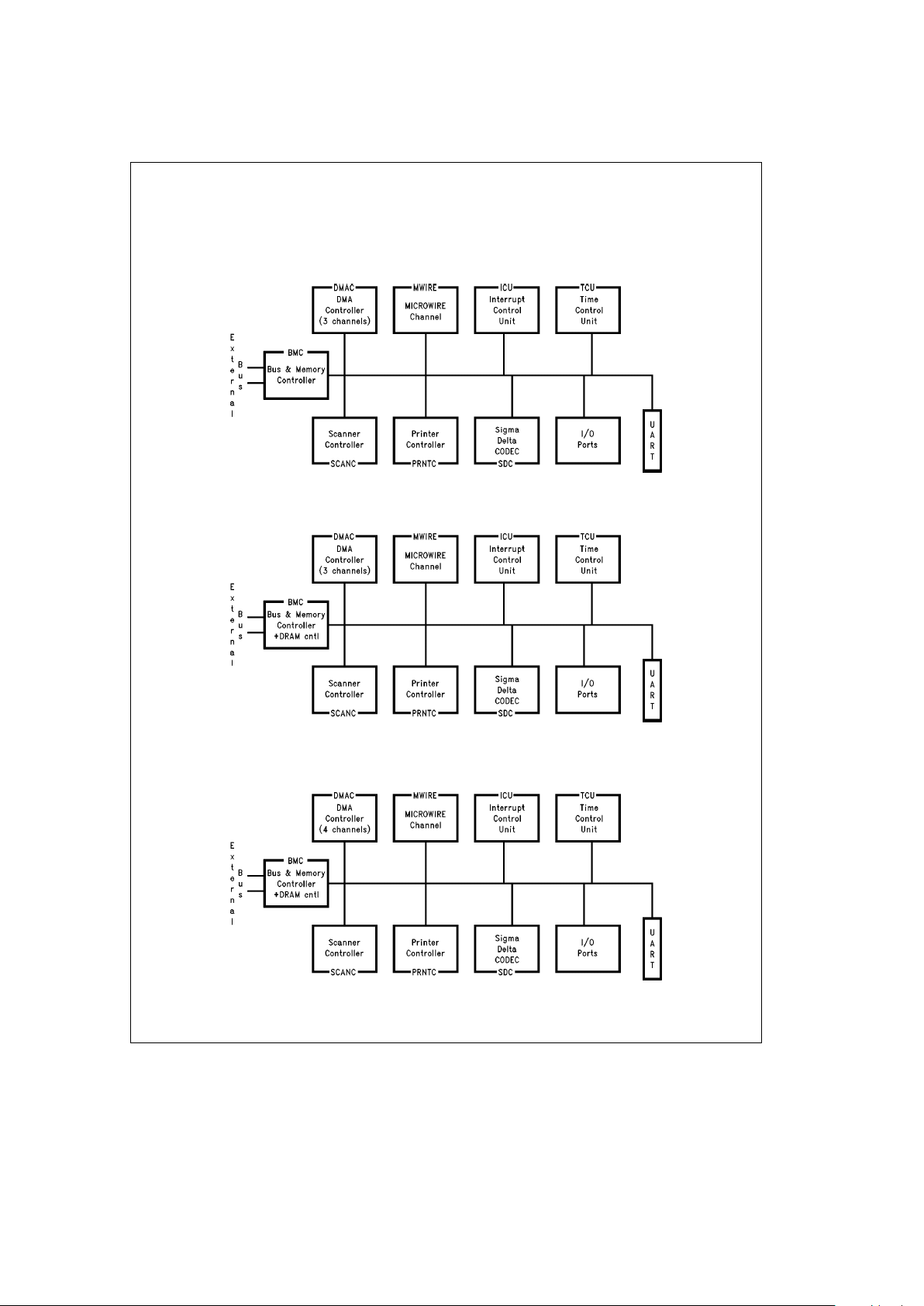
1.2 MODULE DIAGRAM
The various functions of the NS32FX100, NS32FV100 and
NS32FX200 are performed by on-chip modules as shown
below.
The NS32FX100 module diagram is shown in
Figure 1-2.
TL/EE/11331– 3
FIGURE 1-2. NS32FX100 Module Diagram
The NS32FV100 module diagram is shown in
Figure 1-3.
TL/EE/11331– 4
FIGURE 1-3. NS32FV100 Module Diagram
The NS32FX200 module diagram is shown in
Figure 1-4.
TL/EE/11331– 2
FIGURE 1-4. NS32FX200 Module Diagram
7
Page 8

1.0 Fax-System Configuration (Continued)
The NS32FX100 modules, and their functions, are summarized below: For a more detailed description of each module, see the relevant section.
1.2.1 Bus and Memory Controller (BMC)
The Bus and Memory Controller (BMC) interfaces directly to
the NS32FX161, the NS32FV16 or the NS32FX164. It enables the NS32FX100 to respond to both read and write
transactions, and to generate DMA transactions. It divides
the address space into four external zones and generates
wait states, and idle cycles, according to the addressed
zone, type of transaction and the programmed wait value.
The memory controller directly interfaces to ROMs and
SRAMs. The memory controllers of the NS32FX200 and the
NS32FV100, in addition, directly interface to DRAMs.
1.2.2 Timing Control Unit (TCU)
The Timing Control Unit (TCU) contains three blocks. An
oscillators block generates the CPU high-speed clock and
the time-keeper clock. The TCU module keeps trace of
elapsed time during all operation modes. A counters block
contains timers/counters for the various FAX-system controller operations.
1.2.3 Sigma-Delta CODEC (SDC)
The Sigma-Delta CODEC (SDC) interfaces with the telephone line via an external Data Access Arrangement (DAA),
performing analog-to-digital and digital-to-analog conversions, data sampling and buffering. Off-hook control and
ring-detect monitoring are performed by the Ports module.
1.2.4 Scanner Controller (SCANC)
The Scanner Controller (SCANC) contains the video handling block, the scanner signals generator and the stepper
motor control block. The block includes both analog and
digital circuits. It uses DMA channel 0 to fetch a reference
line from memory and DMA channel 2 to store the digitized
video data to memory.
1.2.5 Printer Controller (PRNTC)
The Printer Controller (PRNTC) contains the printer bitmap
shifter, the stepper motor control block, the temperaturesensing block and the thermal print head control block. It
uses DMA channel 1 to fetch the bitmap from memory.
1.2.6 DMA Controller (DMAC)
NS32FX200. The DMA Controller (DMAC) provides four in-
dependent channels for transferring blocks of data between
memory and I/O devices, with minimal CPU intervention.
Two channels are used for scanner control, one for printer
control and one is available for external usage.
NS32FX100, NS32FV100. The DMA Controller (DMAC) provides three independent channels for transferring blocks of
data between memory and I/O devices, with minimal CPU
intervention. Two channels are used for scanner control,
one for printer control.
1.2.7 Universal Asynchronous Receiver-Transmitter
(UART)
The Universal Asynchronous Receiver-Transmitter (UART)
supports 7-bit or 8-bit data formats, with or without parity,
with or without hardware flow control, and with one or two
stop bits. The baud rate is generated on-chip, under software control.
1.2.8 MICROWIRE (MWIRE)
The MWIRE is a serial synchronous communication interface. It enables the CPU to interface with any of National
Semiconductor’s chips which support MWIRE, such as
COP400, COP800 and EEPROMs. The MWIRE interface
consists of three signalsÐserial data in, serial data out, and
shift clock. Several devices can share the MWIRE channel
using selection signals provided by the Ports module.
1.2.9 Interrupt Control Unit (ICU)
The Interrupt Control Unit (ICU) receives internal and external interrupt sources and generates an interrupt to the CPU
when required. Priority is allocated according to a predetermined scheme. The ICU supports programmable triggering
mode and polarity. Each interrupt source can be individually
enabled or disabled. Pending interrupts can be polled, regardless of whether they are enabled or disabled.
1.2.10 Ports
The Ports module controls the usage of general-purpose
input and output pins. The pins are shared with other modules, and can be configured either as general-purpose I/O
pins or as pins that belong to other modules. An input port
always holds the current value/state of its associated pins.
Output pins can be enabled or disabled (TRI-STATE
É
).
The number of general-purpose output pins can easily be
increased using an external latch (e.g., DM74LS373).
1.3 OPERATION MODES
The NS32FX100 operates in one of three modes:
#
Normal Mode: The CPU operates at the full clock fre-
quency. Maximum current consumption is 200 mA.
#
Power Save Mode: The CPU runs at 1/16 of the Normal
mode frequency. DMA channels must
be disabled, output ports must be TRISTATE, and MCFG, except for bit 0,
must be cleared. Maximum current
consumption is 17 mA.
#
Freeze Mode: The CPU is frozen by active reset and
frozen clock; it is not connected to the
backup battery. The NS32FX100 chip
keeps track of elapsed time. The
NS32FX200 and NS32FV100 can, if
required, refresh the memories. Maximum current consumption is 1 mA with
refresh, and 0.1 mA without refresh.
In normal operation, (see
Figure 1-5
) when reset is asserted, the NS32FX100 enters S6 of the Power Save mode.
Switching from Power Save to Normal mode is carried out
by software.
An RC circuit may be used to generate the CPU’s input
reset signal. The WATCHDOG trap signal (WDT), generated
by the NS32FX100, may also force active CPU’s input reset.
The NS32FX100 receives its reset from the CPU output reset signal. This line should be pulled down by a resistor to
force reset in case the CPU is not powered.
Failure of the main power source is detected externally (see
Figure 1-6
). The CPU is notified by a non-maskable interrupt. The NS32FX100 is also notified that power has failed,
through the PFAIL
input pin. The NS32FX100 power source
should be externally switched to the backup battery. The
8
Page 9
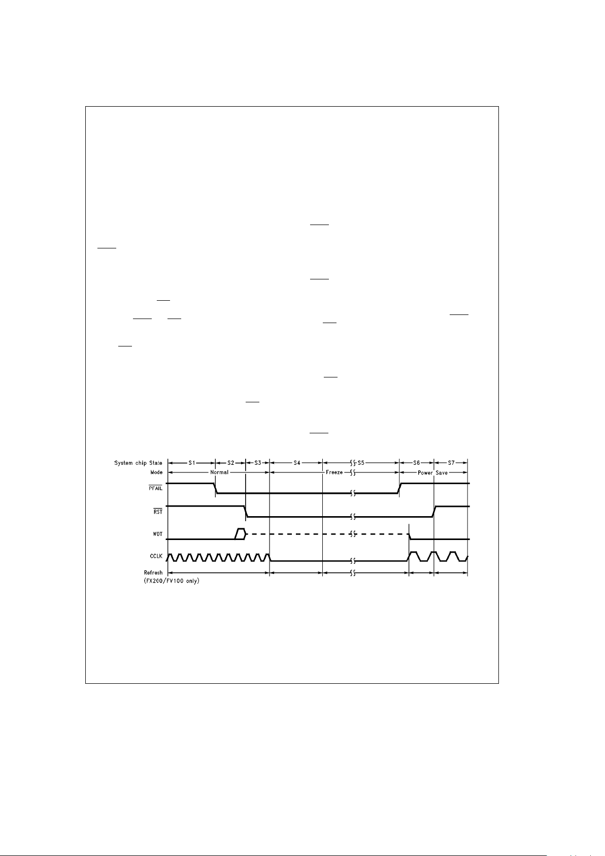
1.0 Fax-System Configuration (Continued)
power-fail input is asynchronous. It is recognized by the
NS32FX100 during cycles in which the input setup-time requirement is satisfied.
Switching from Normal mode to Power Save mode, and vice
versa, must always be carried out using the NS32FX100
explicitly. The clock scaling option of the CPU should not be
used for this purpose.
1.3.1 Functionality
State S1: Normal Mode. The system operates at the full
clock frequency. The NS32FX100 is powered by the main
power supply. Software can switch the system to state S7,
Power Save Mode.
The NS32FX100 switches to state S2, Power Fail, when
PFAIL
is asserted.
State S2: Power Fail. In this state, the CPU enters an NMI
handler, in which the software performs all the bookkeeping
required for recovery and switches to full clock frequency.
The software should write H’80 to MCFG. Once finished,
the software activates the WATCHDOG trap output signal,
which asserts the RST
input of the CPU by writing three
times to the WATCHDOG.
When both PFAIL
and RST are active, the NS32FX100 and
the RAM must be powered from a battery. The CPU can be
powered down.
When RST
is detected, the system chip goes from S2 to
one of the following states:
State S3, if DRAM refresh is enabled (only in NS32FV100
and NS32FX200).
State S5, if no DRAM refresh is needed (NS32FX100Ðal-
ways).
State S3: Complete Refresh Transaction. If RST
is detected, while refresh is enabled, in state S2, a refresh transaction is performed. The system chip then switches to state
S4.
State S4: Freeze and Refresh. In this state, the system
chip de-activates the fast crystal oscillator and freezes the
CCLK clock. Only the Elapsed Time Counter and the DRAM
refresh generator are functional.
When the ETC count reaches zero, the state machine
switches to state S5, and refresh transactions are stopped.
Thus, the contents of the DRAM can be kept for a predefined period (software programmable). If the power failure
lasts longer than this period, the system should disconnect
the DRAM and leave only the ETC, and possibly an SRAM
device, connected to the battery.
If PFAIL
goes high, the state machine switches to state S6,
Power Restore.
State S5: FreezeÐNo Refresh. In this state only the ETC
counter is activeÐcounting the duration of the power failure. In this state the NS32FX100 functions with a supply
voltage as low as 3V.
If PFAIL
goes high, the state machine switches to state S6,
Power Restore.
State S6: Power Restore. This state can be entered either
from Freeze Mode or during normal operation when reset is
asserted. When entering from Freeze Mode (PFAIL
goes
high), RST
is kept low for a few milliseconds by an external
circuit. During this time, the fast crystal oscillator is activated
and the CPU and NS32FX100 clocks are synchronized.
If refresh is enabled, the system chip will initiate refresh
transactions during this timeÐthe refresh rate is forced to a
default value.
When RST
goes high, the NS32FX100 switches to state S7,
Power Save Mode.
State S7: Power Save Mode. The CPU runs at a slow frequencyÐ1/16 of the Normal Mode frequency.
The system can swtich to S1, Normal Mode, under software
control.
If PFAIL
input is asserted, the NS32FX100 switches to state
S2, Power Fail.
TL/EE/11331– 5
FIGURE 1-5. System Chip States and Operation Modes
9
Page 10
2.0 Architecture
2.1 MCFGÐMODULE CONFIGURATION REGISTER
The software can configure some of the NS32FX100 major
operation modes by programming the Module Configuration
Register (MCFG). Some of the bits in this register are also
used to initialize the TPH block in the PRNTC, the bitmap
shfiter block in the PRNTC and the scanner module. When
a bit in the MCFG is ‘‘0’’, the associated module is idle.
Setting a bit to ‘‘1’’ enables the operation of the associated
module. Prior to activating a module, its appropriate registers must be initialized by software.
15 6 5 4 3 2 1 0
res ESDC EDMA0 ESCAN EPBMS ETPHB ECOUNT
ECOUNT: Enable internal counters of the TCU module.
Once set, this bit can not be cleared by software.
The TCU counters, except TIMER and WDC,
must be initialized prior to setting this bit since
they start working when the ECOUNT bit is set.
ETPHB: Enable Thermal Print-Head Block of the PRNTC
module. The strobe-on and strobe-off counters
of this block must be initialized prior to setting
this bit to ‘‘1’’.
EPBMS: Enable Bitmap Shifter Block of the PRNTC mod-
ule. Clearing this bit is treated, by the Bitmap
Shifter, as a hardware reset. The block starts operating when this bit is set. When disabled, DMA
channel 1 uses the printer PCLK/DMRQ1
pin.
ESCAN: Enable Scanner module. Clearing this bit is treat-
ed, by the Scanner Controller, as a hardware reset. The module starts operating when this bit is
set. When cleared to ‘‘0’’, DMA channel 2 uses
the scanner pins and interrupt.
EDMA0: Enable scanner usage of DMA channel 0. When
cleared to ‘‘0’’, DMA channel 0 uses the scanner
pins and interrupt.
ESDC: Enable Sigma-Delta CODEC module. When this
bit is set the SDC operation takes place as described in Section 2.3.
Upon reset the non reserved bits of the MCFG are cleared
to ‘‘0’’, thus disabling the above modules and options.
2.2 TIMING CONTROL UNIT (TCU)
2.2.1 Features
#
Generation and control of clock running frequency
#
CPU and NS32FX100 synchronization by Phase Lock
Loop (PLL)
#
Fixed System-Tick interrupt of 100 Hz
#
WATCHDOG
#
Timer
#
Buzzer
#
Freeze mode
2.2.2 Operation
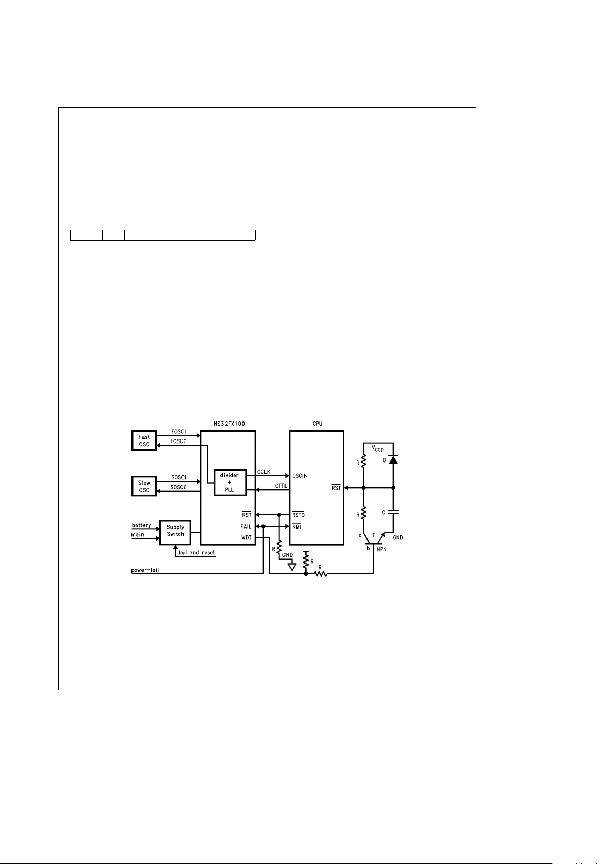
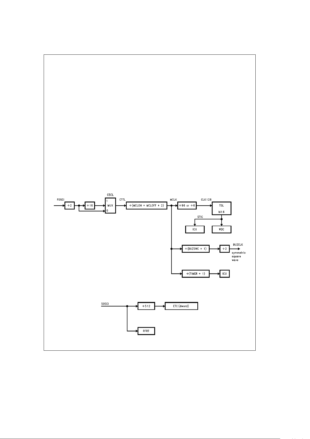
The Timing Control Unit (TCU) is responsible for generating
the clocks, used for the various timing and counting functions in the system, and for freeze mode operation.
Figure
2-1
shows how the clocks are connected in an NS32FX100-
based FAX system.
TL/EE/11331– 6
FIGURE 2-1. Clocks and Traps Connectivity
10
Page 11
2.0 Architecture (Continued)
2.2.2.1 External Clocks
The TCU contains two oscillators, the high-speed oscillator
and the low-speed oscillator. The high-speed oscillator is
the FAX system clocking source. It generates the CPU clock
and, after division, clocks for the Sigma-Delta CODEC,
scanner, printer and serial communications channels. A
high-speed clock signal is input to the NS32FX100, from an
external crystal, through the FOSCI pin. The NS32FX100
uses this signal to generate the CCLK clock, which serves
as the input clock to the CPU. The CPU then divides CCLK
by two, and generates CTTL which serves as the bus clock.
The NS32FX100 includes a PLL to ensure synchronization
between the NS32FX100 clocks and the CPU. CTTL is used
to close the PLL loop and enable tracking of the CPU internal clocks.
The low-speed oscillator, which gets its input through the
SOSCI pin, is used to keep track of elapsed time and to
operate the refresh requester. This oscillator operates in
Normal mode, as well as in Power Save and Freeze modes.
The NS32FX100 controls the CPU running frequency. It
may reduce the frequency by dividing CCLK by 16. To ensure accurate tracking of the CTTL phase by the
NS32FX100, clock division should be carried out via the
NS32FX100, and the power save mode of the CPU should
not be used.
The slow oscillator, which operates during Normal, Power
Save and Freeze modes, can be a 32.768 kHz oscillator for
systems with memory refresh rate of up to 8 kHz. Systems
with memory refresh rate higher than 8 kHz should use a
slow oscillator of 455 kHz.
2.2.2.2 Internal Clocks
The TCU module generates a 1.2288 MHz Master Clock
(MCLK). MCLK is generated by a programmable divider,
which divides the CTTL input clock. The MCLK clock is used
for synchronization throughout the NSFX100-based FAX
system. In particular, the following are derived from MCLK:
#
CLK128ÐA 12.8 kHz clock
#
Time-Slots generator (TSL)ÐAn 8-bit down counter fed
by CLK128
The Time-Slots generator performs two functions:
#
Division of each 20 ms period into 256 time slots
#
Generation of a 100 Hz System Tick (STIC)
The time slots are used to synchronize the various components of the FAX system, e.g., the printer and scanner with
their respective motors.
The System Tick is used by both the Interrupt Control Unit
(ICU), for generating an interrupt, and by the WATCHDOG
counter, as described in Section 2.2.3.
Several registers are provided, to control and use the TCU
and I/O signals. These registers are described in Section
2.2.3.
Note 1: When CSCLe1, CLK128 is generated by dividing MCLK by 6.
Note 2: When CSCL
e
0, CLK128 is generated by dividing MCLK by 96.
(MCLK is 1.2288 MHz; refer to Table I for MCLON and MCLOFF values)
TL/EE/11331– 7
Note 3: CLK128 is always 12,800 Hz and STIC is always 100 Hz.
FIGURE 2-2. High Speed Oscillator Clocks
TL/EE/11331– 8
FIGURE 2-3. Low Speed Oscillator Clocks
11
Page 12

2.0 Architecture (Continued)
2.2.3 Registers
CSCL: CCLK (CPU Input Clock) Scale register.
7543 0
res F res
F: Controls the CCLK frequency.
1: The CCLK frequency is the FOSCI input
frequency divided by 16.
0: The CCLK frequency is the FOSCI input
frequency.
Upon reset F is set to ‘‘1’’.
res: Reserved
MCLOFF: MCLK Off Time. 8-bit register.
MCLOFF should be set to a fixed value, as
shown in Table I, as a function of CTTL in normal operation mode, to generate a 1.2288 MHz
clock, thus controlling the CTTL duty cycle.
MCLON: MCLK On Time. 8-bit register.
MCLON should be set to a fixed value, as
shown in Table I, as a function of CTTL in normal operation mode, to generate a 1.2288 MHz
clock, thus controlling the CTTL duty cycle.
TABLE 2-1. CTTL, MCLON and MCLOFF Values
CTTL (MHz) MCLON MCLOFF
14.7456 5 5
15.9744 6 5
17.2032 6 6
18.4320 7 6
19.6608 7 7
20.8896 8 7
22.1184 8 8
23.3472 9 8
24.5760 9 9
TIMER: Programmable Timer.
15 0
TIMER
TIMER: The actual counter bits.
TIMER is a programmable, retriggerable, down counter
which generates an interrupt pulse after a programmable
number of MCLK cycles. When it goes below zero it stops
counting and holds the value 0x0ffff. If a new value is written
to the TIMER before it reaches zero, it starts counting down
from this new value. Reading TIMER gives its current contents.
Each bit in the TIMER register stands for 0.8 ms (1/1.2288
MHz), thus the counter may represent the maximum value
of 0.8 x 2
16
ms.
Writing ‘‘0’’ to the timer is not allowed.
BUZCFG: Buzzer Configuration register.
765 0
BCTRL res
BCTRL: Used to control the BUZCLK pin.
00 : BUZCLK pin
e
0.
01 : BUZCLK pine1.
10 : BUZCLK pinesymmetric square wave,
according to BUZSWC register.
11 : Reserved.
BUZSWC: Buzzer Square Wave Counter. 16-bit register.
Used for dividing MCLK to generate a symmetric
square wave on the BUZCLK pin, as follows:
BUZCLK frequency
e
MCLK/(2 *
BUZSWC
a
2).
WDC: WATCHDOG Counter. 8-bit register.
The WATCHDOG Counter (WDC) is a down
counter that counts STIC pulses. The counter
generates a trap signal, on the WATCHDOG
Trap (WDT) pin, if the counter reaches zero, or if
WDC is written into more than once per STIC
cycle. After reset WDC is idle (not counting). It
starts counting after it is first written, starting
from the value that is written into it. Once started, WDC can be stopped only by a hardware
reset.
The WATCHDOG counts STIC pulses which are
generated by the TCU. Therefore the WATCHDOG is functional only when the TCU’s counters
are enabled by the MCFG.ECOUNT bit.
Writing ‘‘0’’ to the timer is not allowed.
TSL: Time Slot down counter. 8-bit, read only.
Holds the current time slot. Upon reset the TSL
bits are set to ‘‘1’’.
ETC: Elapsed Time Counter. A 32-bit down counter
that counts at a rate of the slow clock (SOSCI)
divided by 512.
Accessed as double-word only.
Not affected by reset.
At least four slow-clock cycles are required, between a write and any accesses to ETC, to
avoid unpredictable results.
Successive reads from the ETC may differ from
each other by two.
Example:
Read ETC, value
e
n (correct value should be
n
a
1)
Read ETC, value
ena
2 (correct value).
RFRT: Refresh Rate Control. 8-bit register.
The refresh is set to occur once every (RFRT
a
1) cycles of the slow clock. RFRT must be set to
a minimum value of 3.
The actual refresh transaction may be postponed due to synchronization with the fast clock
and with other memory transactions.
12
Page 13

2.0 Architecture (Continued)
After reset, RFRT is initialized to 6.
Writing to RFRT must be followed by read back
to ensure that the RFRT has, in fact, been updated. This procedure must be repeated until
RFRT is updated (value read
e
value written).
RFRT exists only in the NS32FV100 and the
NS32FX200.
RFEN: Refresh enable
765 0
res EN res
EN 0: No refresh transactions.
1: Refresh transactions are issued by
the chip according to the refresh
rate, selected by RFRT.
After reset EN is set to ‘‘1’’.
RFEN exists only in the NS32FV100 and the
NS32FX200.
2.2.3.1 Usage Recommendations
The ECOUNT bit, in MCFG, must be set to enable TCU
counters operation.
2.3 SIGMA-DELTA CODEC (SDC)
2.3.1 Features
#
16-bit format Analog-to-Digital converter and Digital-toAnalog converter
#
Full and Half Duplex operation
#
Optimized for FAX and DATA Modems
#
Various sampling rates for voice and data applications
#
Total harmonic distortion better thanb70 dB
#
Programmable IIR filters
Ð Programmable transmit filters
Ð Programmable receive filters
Ð Programmable echo canceling filter
#
Programmable gain control
#
Programmable fine timing tuning
#
Digital loop-back mode
#
Reduced CPU load by 12-level transmission FIFO and 12level reception FIFO
2.3.2 Operation
The Sigma Delta CODEC performs high resolution analogto-digital (A/D) and digital-to-analog (D/A) conversions using an over sampling technique. This module is optimized
for use as the analog front end for Digital Signal Processing
(DSP) applications such as modems or voice processing.
The SDC’s main advantage, compared to other A/D and
D/A convertors, is the use of digital circuitry resulting in high
reliability and reduced cost. The SDC solution incorporates
a second-order, digital Sigma-Delta modulator and a noise
shaping technique to improve performance.
The digital parts of the converters are implemented on-chip
and a few external components implement the analog parts.
NSFAX Software package fully supports the SDC. Software
drivers handle both the SDC initialization and data transfers.
National Semiconductor’s modem software is usually provided in binary form, and hence the internal structure of the
SDC is transparent to the user. A detailed description of the
SDC is available only for source-level customers.
2.3.2.1 Block Diagram
The Sigma-Delta CODEC block diagram is shown in
Figure
2-4.
13
Page 14
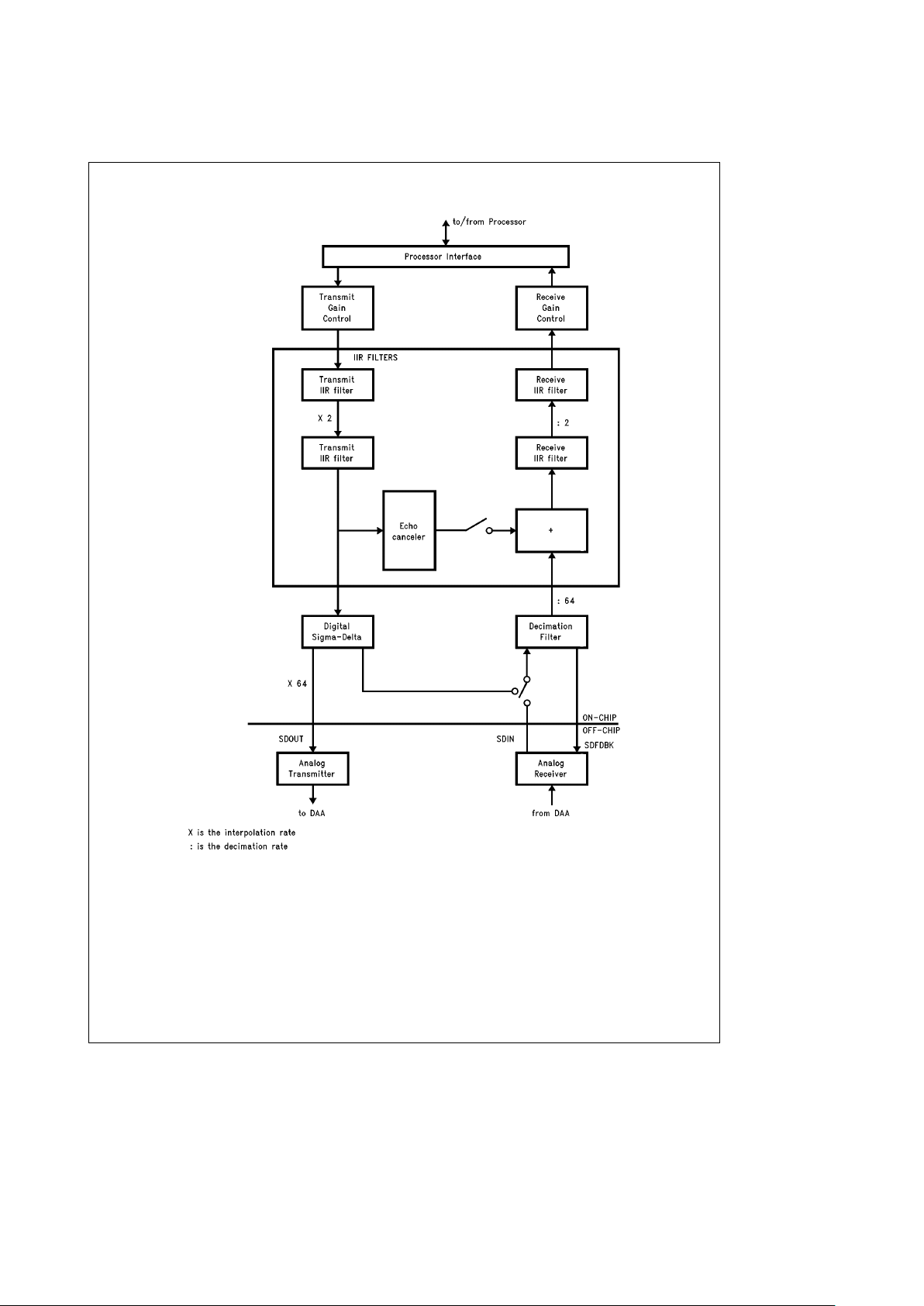
2.0 Architecture (Continued)
TL/EE/11331– 9
FIGURE 2-4. Sigma-Delta Block Diagram
14
Page 15
2.0 Architecture (Continued)
A full Sigma-Delta CODEC includes a digital part and an
analog part. The NS32FX100 includes the digital part, and
the analog part should be implemented externally.
2.3.2.2 On-Chip Digital Blocks
Sigma-Delta Over Sampling Rate (OSR) is 128 times the
Sampling Rate (SR). Some Sigma-Delta blocks use also
Double Sampling Rate (DSR).
For communication applications the SR is 9.6 kHz, DSR is
19.2 kHz and the OSR is 1.2288 MHz. For voice applications the SR is 8 kHz, DSR is 16 kHz and the OSR is
1.024 MHz.
DF (Decimation Filter)ÐReceives 1-bit stream at OSR and
decimates it to 16-bit at DSR.
IIR FiltersÐThe IIR filters include Transmission, Reception
and Echo-canceler programmable filters. The Echo-canceling filter can be bypassed.
The Transmission IIR includes two filters. The first
filter operates at SR. The second filter interpolates
the data rate by two. Thus the filter operates at
DSR.
The Reception IIR includes two filters. The first filter
operates at DSR and decimates the data rate by
two. Thus the second filter operates at SR.
The Echo-canceler filter works at DSR. This filter is
used to cancel the echo path.
Receive Gain Control (RGC)ÐAmplifies or attenuates the
received data, to achieve the required signal level, controlled by software Automatic Gain Control (AGC).
Transmit Gain Control (TGC)ÐAttenuates the transmitted
data, to achieve the required signal level, controlled by software Automatic Gain Control (AGC).
Digital Sigma-Delta (DSDM)ÐTransforms the 16-bit transmitted data at DSR into a 1-bit stream at OSR. A second-order digital Sigma-Delta circuit performs this function.
Processor Interface (PI)ÐContains the SDC control and
data registers, a 12-level transmission FIFO, a 12-level reception FIFO and a clock divider unit.
2.3.3 Programmable Functions
The Sigma-Delta programming model consists of the following elements:
#
IIR coefficients memory
#
Data registers
#
Control registers
2.3.3.1 Sigma-Delta ON/OFF
The SDC module is enabled by MCFG.ESDC control bit.
When MCFG.ESDC is ‘‘0’’ the SDC module is disabled.
The user can access all SDC memory-mapped addresses
(IIR coefficients and SDC registers) only while MCFG.ESDC
is active. Any attempt to access SDC memory-mapped addresses while MCFG.ESDC is ‘‘0’’ will cause an unpredictable result.
To turn off SDC, turn off receive mode (SDCNTL.RE
e
0)
and transmit mode (SDCNTL.TE
e
0) and only then clear
MCFG.ESDC to ‘‘0’’.
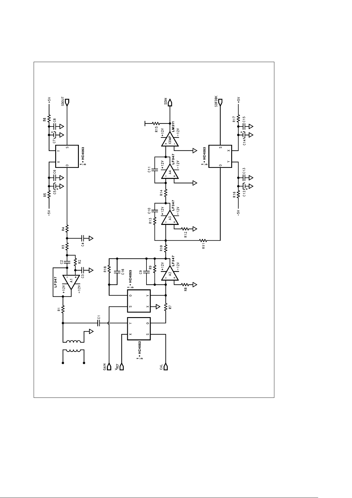
2.3.4 Off-Chip Analog Circuits
The circuit required to connect the SDC on-chip module to a
2-wire line is shown in
Figure 2-5
. The components are de-
tailed in the following table:
TABLE 2-2. Component Values
Component Value Tolerance
R1 600X 1%
R2 47 kX 5%
R3 47 kX 5%
R4 47 kX 5%
R5 330X 5%
R6 330X 5%
R7 15.4 kX 1%
R8 56 kX 5%
R9 100 kX 5%
R10 22 kX 5%
R11 22 kX 5%
R12 56 kX 5%
R13 5.1 kX 5%
R14 5.6 kX 5%
R15 1.0 kX 5%
R16 330X 5%
R17 330X 5%
R18 56 kX 5%
C1 0.1 mF 10%
C2 3.3 nF 10%
C3 100 pF 10%
C4 1 nF 10%
C5 22 mF 10%
C6 0.1 mF 10%
C7 22 mF 10%
C8 0.1 mF 10%
C9 47 pF 10%
C10 330 pF 10%
C11 200 pF 10%
C12 22 mF 10%
C13 0.1 mF 10%
C14 22 mF 10%
C15 0.1 mF 10%
C16 100 pF 10%
15
Page 16
2.0 Architecture (Continued)
TL/EE/11331– 10
FIGURE 2-5. SDC Off-Chip Analog Circuit
16
Page 17
2.0 Architecture (Continued)
2.3.4.1 Analog Transmitter
The input to the transmit analog circuit is the serial bit
stream at OSR, which is generated by DSDM. This serial bit
stream is fed to a 1-bit D/A converter. This D/A converter is
implemented by an analog switch, which selects either
a
5V
or
b
5V inputs. These voltages are filtered by an RC, lowfrequency, Low Pass Filter (LPF), to filter supply noise, and
to avoid crosstalk between the transmit and receive circuits.
The D/A output is filtered, by a three pole LPF with unity
gain, to attenuate the out-of-band quantization noise. The
output of the LPF passes through a 600X resistor.
2.3.4.2 Analog Receiver
The reception analog circuit obtains its analog input signal
from an isolation transformer. The signal passes through a
buffer amplifier, and then enters the Sigma Delta second
order loop. The amplifier has two gain levels. One gain level
provides a total gain of 0 dB and the second level provides
a total gain of 9 dB. The two gain level are controlled by the
GAIN signal.
The Sigma Delta second order loop contains two integrators
and a comparator to zero. The comparator output is the
SDIN input to the on-chip Sigma Delta part. SDIN is sampled on-chip at OSR, is passed to the digital filters and returns as feedback (SDFDBK pin) to the analog part. This
feedback enters a 1-bit D/A converter. This D/A converter
is implemented by an analog switch, which selects either
a
5V orb5V inputs. These voltages are filtered by an RC
low frequency LPF, to reduce supply noise, and to avoid
crosstalk between the transmit and receive circuits. The
feedback is an input to the first integrator unit.
The receiver analog circuit can be calibrated by receiving a
known reference voltage. When the circuit is calibrated, the
receiver input signal is a known reference voltage (V
REF
),
otherwise the receiver input is the input signal from the isolation transformer.
2.3.5 Registers
The following is a partial list of registers. For a full list see
the detailed SD documentation, available to source-level
customers.
SDTX Sigma-Delta Transmit Data. This register is the
transmit FIFO port. Any attempt to read from this
register will cause an unpredictable result.
SDRX Sigma-Delta Transmit Data. This register is the re-
ceive FIFO port. Any attempt to write to this register will cause an unpredictable result.
SDCNTL Control register
15 13 12 11 7 6 5 4 3 2 1 0
N/A N/A PRES N/A TE N/A RE N/A
Upon reset SDCNTL.PRES is loaded at the minimum prescale value in Full-duplex mode, ‘‘01001’’. All other implemented bits of SDCNTL are cleared to ‘‘0’’.
NOTE: Bits marked N/A are available only for source-level customers. For
other customers, they must not be modified.
RE Enables or disables receive mode.
0 : Receive mode is disabled.
1 : Receive mode is enabled.
TE Enables or disables transmit mode.
0 : Transmit mode is disabled.
1 : Transmit mode is enabled.
PRES CTTL prescale. The SDC over-sampling rate is gen-
erated by dividing the CTTL clock by a pre-scale divider. The PRES value is calculated as follows:
PRES
e
[
(CTTL/OSR) - 1].
Some examples for sample rate 9.6 kHz and 8 kHz are given below:
CTTL Frequency CTTL Frequency
SDCNTL.PRES (Sample Rate (Sample Rate
9.6 kHz) 8.0 kHz)
01011 14.7456 MHz 12.2880 MHz
01110 18.4320 MHz 15.3600 MHz
01111 19.6608 MHz 16.3840 MHz
10000 20.8896 MHz 17.4080 MHz
10001 22.1184 MHz 18.4320 MHz
10010 23.3472 MHz 19.4560 MHz
10011 24.5760 MHz 20.4800 MHz
SDFTM Fine Timing register.
74320
res ADV STEP
STEP Advance or delay steps amount (0–7)
ADV Advance direction
0: Delay mode is enabled
1: Advance mode is enabled
Writing to this register, while SDCNTL.RE is active, is allowed only if SDFTM.STEP is equal to a
‘‘0’’.
Writing to this register, while both SDCNTL.RE is
active and SDFTM.STEP is not ‘‘0’’, will cause an
unpredictable result.
While SDCNTL.RE is active, this register holds
the number of advance or delay steps yet to be
executed.
SDRGC Receive Gain Control register. Used to amplify or
attenuate the receive IIR output samples. The
value to be written in SDRGC register is 128
c
10
(Gain/20)
, rounded to the nearest integer num-
ber.
Some examples are given in the following table:
Gain (dB) SDRGC
b
18 0x0010
b
17.5 0x0011
..
..
0 0x0080
0.1 0x0081
..
..
48.0 0x7D98
17
Page 18

2.0 Architecture (Continued)
SDTGC Transmit Gain Control register. Used to attenuate
the transmit IIR input samples. The value to be
written in SDTGC register is 16384
c
10
(Gain/20)
,
rounded to the nearest integer number.
Some examples are given in the following table:
Gain (dB) SDTGC
b
42 0x0082
b
41.9 0x0084
..
..
0 0x4000
SDSTAT Status Register. Provides information about the
status of the Sigma-Delta operation.
76543210
TSAT RSAT TFNE RFNE TERR RERR TIRQ RIRQ
RIRQ When ‘‘1’’ during receive enable (SDCNTL.REe1),
it indicates that N or more samples are ready in the
receive FIFO. This bit will remain high as long as the
number of samples is greater than, or equal to, N. If
this bit is not masked by SDMASK.RIRQ it will cause
an interrupt.
TIRQ When ‘‘1’’ during transmit enable (SDCNTL.TE
e
1),
it indicates that less than N samples are ready in the
transmit FIFO. This bit will remain high as long as
the number of samples is less than N. If this bit is not
masked by SDMASK.TIRQ it will cause an interrupt.
RERR When ‘‘1’’ during receive enable (SDCNTL.RE
e
1) it
indicates an attempt to read an empty receive FIFO,
or incoming sample when the receive FIFO is full. If
this bit is not masked by SDMASK.RERR it will
cause an interrupt.
TERR When ‘‘1’’ during transmit enable (SDCNTL.TE
e
1)
it indicates an attempt to read from an empty transmit FIFO, or writing to a full transmit FIFO. If this bit
is not masked by SDMASK.TERR it will cause an
interrupt.
TFNE Transmit FIFO Not Empty, when ‘‘0’’ indicates that
the transmit FIFO is empty.
RFNE Receive FIFO Not Empty, when ‘‘0’’ indicates that
the receive FIFO empty.
RSAT Reception Saturation. This bit is set to ‘‘1’’, whenev-
er a saturation value is created in the receive IIR
(including the echo-canceling filter, when enabled)
or in the receive gain control logic.
TSAT Transmit Saturation. This bit is set to ‘‘1’’, whenever
a saturation value is created in the transmission IIR
or in DSDM.
Upon reset all implemented bits in the SDSTAT register are cleared to ‘‘0’’.
SDMASK Mask Register. Enables masking of SDC inter-
rupts.
7 43210
res TERR RERR TIRQ RIRQ
RIRQ Mask Receive Interrupt Request.
0 : SDSTAT.RIRQ will not cause an interrupt.
1 : SDSTAT.RIRQ will cause an interrupt.
TIRQ Mask Transmit Interrupt Request.
0 : SDSTAT.TIRQ will not cause an interrupt.
1 : SDSTAT.TIRQ will cause an interrupt.
RERR Mask Receive Error.
0 : SDSTAT.RER will not cause an interrupt.
1 : SDSTAT.RER will cause an interrupt.
TERR Mask Transmit Error.
0 : SDSTAT.TER will not cause an interrupt.
1 : SDSTAT.TER will cause an interrupt.
2.3.6 Usage Recommendations
The SDC should be enabled (by setting the SDC bit in the
MCFG register to ‘‘1’’) before programming SDMASK and
SDCNTL.
2.4 SCANNER CONTROLLER (SCANC)
2.4.1 Features
#
Programmable generation of control signals which support a wide range of Charge Coupled Device (CCD) and
Contact Image Sensor (CIS) scanners
#
Supports line scan times of 2.5 ms, 5 ms, 10 ms and
20 ms
#
On-Chip shading-correction circuitry, using reference line
values stored in the system RAM, via DMA channel 0
#
On-Chip dithering and Gamma correction circuit of 16
grey levels. (64 grey levels in NS32FX200)
#
Support for Automatic Background Control (ABC) and
edge enhancement with external circuitry
#
On-Chip multiplying Digital-to-Analog Converter (DAC)
for compensation of scanner offset
#
Automatic writing of scanned bitmap to memory via DMA
channel 2
#
Optional bypass of on-chip video-data generation to support external image enhancement
2.4.2 Operation
The Scanner Controller Module (SCANC) consists of a
scanner signals generator block, a video handling block
(shading compensation, dithering and bitmap accumulation)
and a stepper motor control block. The module includes
analog and digital circuits. It uses two DMA channelsÐone
for fetching a reference line and one for storing the digitized
video data. The module is synchronized with the TCU module. The operation of SCANC, and the allocation of DMA
channels 0 and 2 to the Scanner Controller or for external
usage, are controlled by the Module Configuration Register
(MCFG). The module’s minimum operation frequency is
14.7456 MHz (i.e., it can not operate in Power Save mode).
Some of the Scanner signals can be assigned to an I/O port
when the Scanner is not used (e.g., after reset).
18
Page 19
2.0 Architecture (Continued)
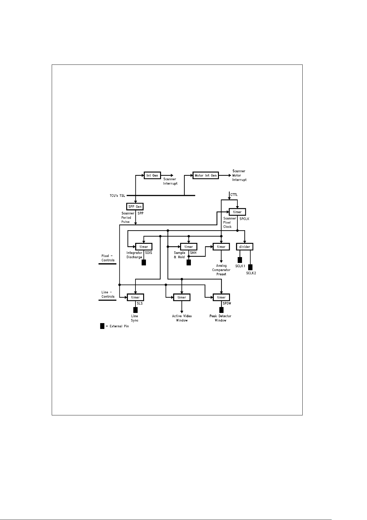
2.4.2.1 Scanner Signals Generator Block
This block generates the timing control signals required by
CIS and CCD scanners. Scanners with line scan time of
2.5 ms, 5 ms, 10 ms or 20 ms are supported. This period is
derived from the TCU module’s time-slots (generated by the
TCU dividing each 20 ms into 256 time-slots).
The block generates the following signals:
Ð Scanner Period Pulse (SPP), an internal synchronization
pulse.
Ð Scanner Pixel Clock (SPCLK), an internal pixel clock (its
frequency is twice the scanner clock).
Ð Pixel clocks (two phasesÐSCLK1 and SCLK2).
Ð Integrator Discharge Pulse (SDIS).
Ð Sample and Hold control clock (SNH). Used to sample
the scanner analog video signal.
Ð Scan Line Synchronization Pulse (SLS). Indicates the
beginning of a scan line.
Ð Scanner Comparator Preset, an internal initialization sig-
nal for the on-chip analog comparator.
Ð Active window, an internal time frame that controls the
operation of the bitmap generator.
Ð Peak Detector Window (SPDW). One of the Automatic
Background Control (ABC) control signals.
Ð Scanner interrupt pulse.
Ð Scanner motor interrupt pulse.
Each signal is generated by an independently programmed
waveform generator. The flexible waveform definition facilitates the support of different scanner models.
TL/EE/11331– 11
FIGURE 2-6. Block Diagram of Scanner’s Signals Generator Block
19
Page 20
2.0 Architecture (Continued)
2.4.2.2 Scanner Period Pulse (SPP) Generation
The Scanner Period Pulse (SPP) is used to synchronize all
the scanner control signals. It is derived from the time slots
generated by the TCU module (which divides each 20 ms
into 256 time slots).
SPCLK Generation
The internal Scanner Pixel Clock (SPCLK) is generated by
dividing CTTL by a programmable prescale value. The result
is a video clock which is twice the frequency of the scanner
clocks. SPCLK is used for generation of other scanner signals. The value of SPCLK should be determined according
to the scanner specification.
The SPCLK pre-scale divider is reset by each SPP leading
edge. As a result, the first SPCLK cycle after the SPP may
be distorted. Software should program the control registers
SAVWD, SLSD and SPDWD so that the first pixel after the
SPP is ignored.
SCLK1 and SCLK2 Generation
The two scanner clocks, SCLK1 and SCLK2, are generated
by dividing SPCLK by two. SCLK1 is high and SCLK2 is low
after SPP leading edge.
SDIS and SNH Generation
The Integrator Discharge Pulse (SDIS) and the Sample-andHold Control Clock (SNH) are generated by timers which
are clocked by CTTL and triggered by SPCLK. For each of
these signals, the polarity, the delay (between SPCLK and
its leading edge) and the width are software programmable.
The total number of delay and width cycles must not exceed
the number of CTTL cycles in one SPCLK period.
Analog Comparator Preset Generation
The Analog Comparator Preset is an internal signal used to
initialize the on-chip analog comparator. It is generated by a
timer, clocked by CTTL and triggered by SNH leading edge.
TL/EE/11331– 12
Note: In this figure SDIS has inverted polarity (DISPe0).
FIGURE 2-7. Scanner Pixel Control Signals
20
Page 21
2.0 Architecture (Continued)
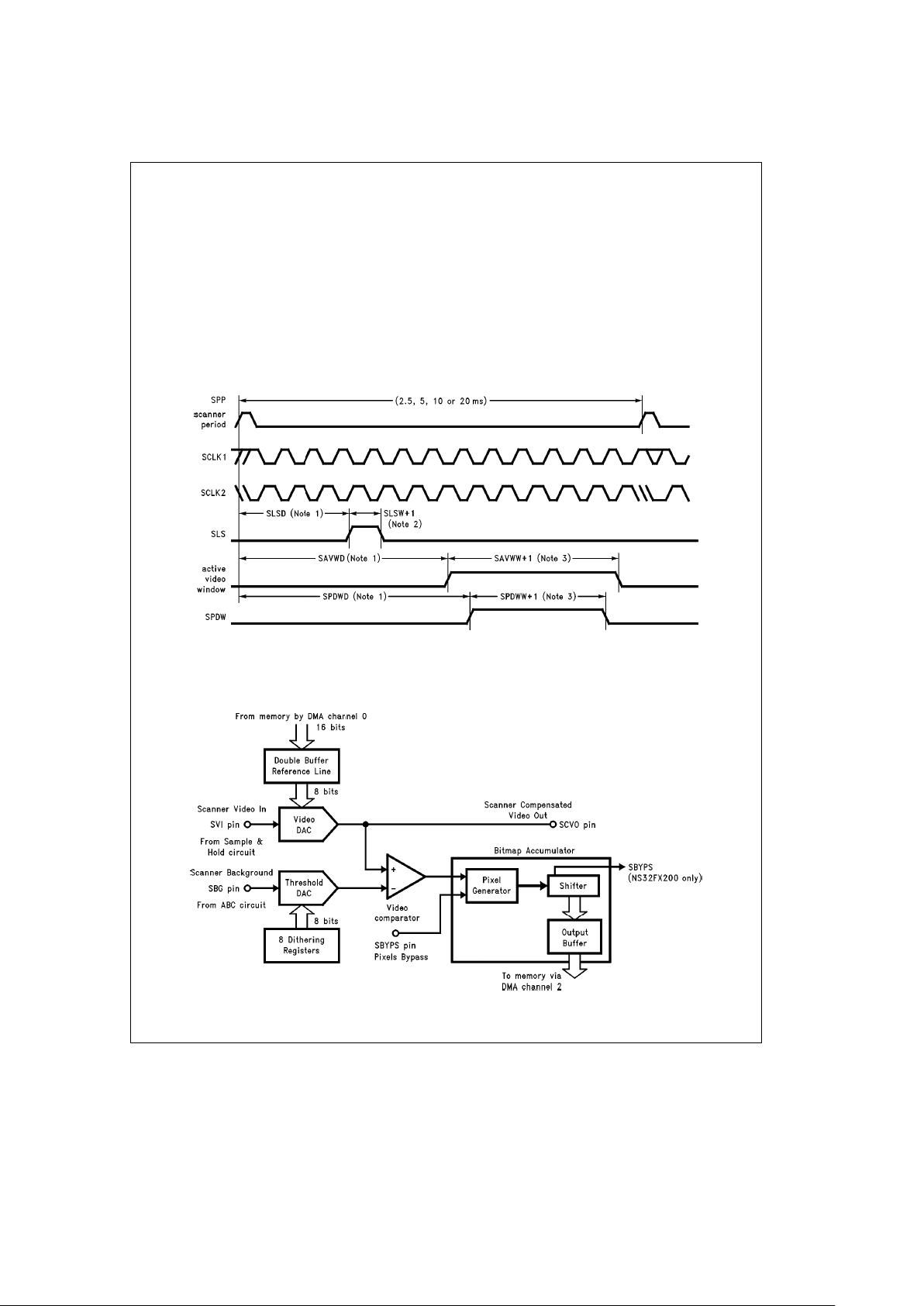
SLS Pulse Generation
Scan Line Sync (SLS) is generated by a timer according to a
calculated delay (in CTTL cycles) from the beginning of the
SPP pulse. The delay between the beginning of SPP and
the leading edge of SLS, SLS pulse width, and SLS polarity
are software programmable.
The first pixel clock after SPP may be distorted. SLS must
be programmed so that this pixel is ignored.
Active Video Window and Peak Detector Window
Generation
The active Video Window, signaling the valid data window,
and the Peak Detector Window, signaling the programmable
window for Automatic Background Control, are generated
by timers which are triggered by SPP and clocked by
SPCLK.
Scanner Interrupt Generation
The scanner interrupt is a rising-edge interrupt, generated at
the beginning of a time slot which is defined by the Scanner
Interrupt Time-Slot register (SITSL).
2.4.2.3 Video Handling Block
The Video Handling Block is an Analog-to-Digital convertor
for the analog video signal. It enables shading, half-toning
and bi-level support with Automatic Background Control
(ABC). It also allows pixel generation control, using external
circuitry.
TL/EE/11331– 13
Note 1: The delay is controlled by the respective register (SLSD, SAVWD or SPDWD).
Note 2: Measured in CTTL cycles.
Note 3: Measured in SPCLK cycles.
FIGURE 2-8. Scanner Period Control Signals
TL/EE/11331– 14
FIGURE 2-9. Block Diagram of Scanner’s Video Handling Block
21
Page 22
2.0 Architecture (Continued)
Video DAC (Shading-Compensation)
The shading-compensation circuit includes an 8-bit multiplying Digital-to-Analog Converter (DAC) that multiplies SVI,
the analog input from an external video sample and hold
circuit, with a digital reference value (white line) fetched by
DMA channel 0. The Video DAC compensates for the input
offset, according to the compensation value in the SVDB
register, and the control bits in the SVHC register. By writing
to the SVDB register, it is possible to control the Video DAC
directly by software. In this case, the same 8-bit value replica should be written to both bytes of the register. When the
compensation value is greater than the input video signal,
the compensated video data signal is ‘‘0’’. The compensated video data, at the output of the video DAC, feeds the
video comparator. It also goes to an external pin (SCVO) to
enable external implementation of an Automatic Background Control (ABC) circuit.
To enable a longer latency for DMA channel 0 operations, a
double buffer is used. DMA cycles are synchronized to the
leading edge of SNH during active video window.
When DMA channel 0 is disabled, the same value should be
written to both bytes of the Scanner Video DAC Buffer
(SVDB) register.
2.4.2.4 Threshold DAC (Dithering and Automatic
Background Control)
The dithering circuit includes an 8-bit multiplying DAC that
multiplies SBG, the input from an external Automatic Background Control (ABC) circuit, with the digital dither value
from one of the eight dither bytes. The threshold DAC has
no output pin and no I
OFF
, internal offset current, but is
otherwise similar to the video DAC.
The block includes a cyclic buffer for 64 grey levels. The
cyclic buffer contains eight bytes, only one of which is accessible at any given time. Any buffer access (software
read, software write or hardware read) causes a cyclic shift
in the buffer after the access is completed. A hardware ac-
cess, on SNH leading edge, loads the value of the accessed
byte to the DAC’s input. Hardware access can take place
only during active video window. Software access is carried
out via the SDITH register. Software may not access the
buffer during active video window. The dither cyclic buffer is
shown in
Figure 2-10.
For a gray-level image, ABC should
be disabled by externally clamping the SBG input to a constant source. For this purpose, an external analog switch,
controlled by any of the Ports module, may be used.
Note: Eight dither registers are available on all system chips. The difference
between the number of supported gray levels lies in the different
characteristics of the associated analog circuits.
TL/EE/11331– 15
FIGURE 2-10. Dither Cyclic Buffer
Video Comparator
The output of the shading-compensation (video) DAC is
compared by the video comparator with the output of the
dithering (threshold) DAC. The comparator feeds the pixel
generator.
Bitmap Accumulator
The bitmap accumulator includes a pixel generator and a
bitmap shift register. It uses DMA channel 2 to store the
bitmap into memory.
22
Page 23

2.0 Architecture (Continued)
Pixel Generator
Pixels may be treated in one of three ways:
No bypass The output of the video comparator is an
image pixel. It may be inverted by the pixel
generator before the pixel is shifted into the
bitmap shifter.
Input bypass (Available in the NS32FX200 only.) The vid-
eo comparator output is bypassed, (the video DAC output is taken through the SCVO
output pin to an external circuit), and an externally generated pixel is taken as the input
to the pixel generator through the SBYPS
pin.
Output bypass (Available in the NS32FX200 only.) As in the
No bypass case, the comparator feeds the
bitmap shifter. In addition, the last sampled
pixel, sampled on the last SNH leading edge
and inverted, is driven onto the SBYPS pin
for optional use by an external circuit (e.g.,
for edge emphasis).
The operation mode of the pixel generator, in the
NS32FX200, is controlled by the Scanner Video Handling
Control register (SVHC) and Port C control registers (PCMS,
PCEN). It must be configured as ‘‘No bypass’’ in the
NS32FX100 and NS32FV100.
No bypass Ð SVHC.BYPASS
e
0 and
PCMS.MS4
e
0.
Input bypass Ð SVHC.BYPASSe1 and
PCMS.MS4
e
1 and
PCEN.EN4
e
0.
Output bypass Ð SVHC.BYPASSe0 and
PCMS.MS4
e
1 and
PCEN.EN4
e
1.
Note that the pin output value is unpredictable if the scanner
module is disabled (MCFG.ESCAN
e
0) while both
PCMS.MS4 and PCEN.EN4 are set.
The pixel generator can be configured to invert a pixel before it is shifted.
Bitmap Shifter
The pixel generator output is accumulated and stored into
memory via DMA channel 2. Pixels are shifted from left to
right i.e. The first pixel in each word is the Least Significant
Bit (LSB). The bitmap is double buffered by the Scanner
Bitmap Shifter (SBMS) and a word buffer between the scanner module and the DMA channel. The shifter operation is
enabled during active window only, and clocked by SNH
leading edge. In order to allow software intervention in collecting the scanner’s bitmap, the shifter is readable by software.
2.4.2.5 Stepper Motor Control Block
The stepper motor is controlled by four phases. The motor
direction and speed is controlled by setting, or clearing,
each phase as scanning progresses. The motor is controlled by setting the time-slots in which the phases should
be changed (in the SMTSL register). When the set time-slot
is reached, an interrupt is generated and the phase values
are updated to the values in the phase register (SMPH) in
the Ports module.
2.4.3 Registers
SPRES: Scanner SPCLK Prescale. 8-bit register.
One SPCLK cycle time equals (SPRES
a
1)
CTTL cycles.
SDISD: Scanner Discharge Delay. Write only. 8-bit reg-
ister.
Controls the delay between the edge of SCLK1
and the leading edge of the SDIS signal. The
delay is (SDISD
a
1) CTTL cycles.
SDISW: Scanner Integrator Discharge Pulse Width.
Write only. 8-bit register.
The width is (SDISW
a
1) CTTL cycles.
SNHD: Scanner Sample and Hold Delay. Write only.
8-bit register.
Controls the delay between the edge of SCLK1
and the leading edge of SNH signal. The delay
is (SNHD
a
1) CTTL cycles.
SNHW: Scanner Sample and Hold Pulse Width. Write
only. 8-bit register.
The width is (SNHW
a
1) CTTL cycles.
SCMPRW: Scanner Comparator Preset Pulse Width. Write
only. 8-bit register.
The width is (SCMPRW
a
1) CTTL cycles.
SLSD: Scanner Line Sync Delay. Write only. 8-bit regis-
ter.
Controls the delay between the Scanner’s Period Pulse (SPP) and the leading edge of the SLS
signal.
SLSW: Line Sync Pulse Width. Write only. 8-bit register.
The width is (SLSW
a
1) CTTL cycles.
SAVWD: Active Video Window Delay. Write only. 16-bit
register.
Controls the delay between the leading edge of
the Scanner’s Period Pulse (SPP) and the beginning of the active video window (number of
ignored pixels).
SAVWW: Active Video Window Width. Write only. 16-bit
register.
The width is (SAVWW
a
1) SPCLK cycles.
SPDWD: Peak Detector Window Delay. Write only. 16-bit
register.
The delay between leading edge of Scanner’s
Period Pulse (SPP) and the beginning of peak
detector window.
SPDWW: Peak Detector Window Width. Write only. 16-bit
register. The width is (SPDWW
a
1) SPCLK cy-
cles.
SGC: Scanner Signals Generator Control register.
23
Page 24

2.0 Architecture (Continued)
743210
res LSPP PDWP SNHP DISP
DISP: Scanner Discharge Pulse Polarity.
0 : Active low
1 : Active high
SNHP: Sample and Hold Pulse Polarity.
0 : Active low
1 : Active high
PDWP: Peak Detector Window Polarity.
0 : Active low
1 : Active high
LSPP: Line Sync Pulse Polarity.
0 : Active low
1 : Active high
SPP: Scanner period pulse. 8-bit register.
7F : Period pulse each 20 ms (TSL
e
255).
BF : Period pulse each 10 ms (TSLe255 and 127).
DF : Period pulse each 5 ms (TSLe255, 63, 127
and 191).
EF : Period pulse each 2.5 ms (TSL
e
255, 31, 63,
95, 127, 159, 191, 223).
SPP must be programmed with one of these four
values, otherwise the period pulse frequency is undefined.
(TSL indicates the appropriate TCU time slot.)
SVHC: Scanner Video handling Control Register.
7654 0
res BYPASS INVERT VDILS
VDILS: Video DAC Input Level Shift.
Number of current steps to be added-to/subtracted-from the input of the Video DAC. This
field is encoded as: Sign bit
a
four magnitude
bits. When the input of the video DAC is to be
incremented, the sign bit, bit 4, should be set to
‘‘1’’. When it is to be decremented, the sign bit
should be ‘‘0’’. Legal values for VDILS are in the
range
1F . . . 10
0 ...0F
INVERT: 0 : Pixel not inverted by the pixel generator
1 : Pixel inverted by the pixel generator
BYPASS: (NS32FX200 only.)
0 : No bypass. The comparator output is received
by the pixel genertor.
1 : Bypass enabled. The SBYPS input is selected
by the pixel generator and the comparator output
is ignored.
Note: Only the NS32FX200 enables bypassing the video
comparator output through the SBYPS pin. BYPASS
must always be cleared to ‘‘0’’ in the NS32FX100 and
NS32FV100.
SVDB: Scanner Video DAC Buffer. 16-bit register.
Holds two bytes of compensation values. The
lower byte is used first and the upper byte is used
for the next pixel.
Normally written by DMA channel 0.
Accessible by software when the DMA channel is
either disabled or not allocated to the scanner
(i.e., MCFG.EDMA0
e
0).
SBMS: Scanner Bitmap Shifter. Read Only. 16-bit regis-
ter.
Pixels are shifted from left to right, i.e., the first
pixel in each word is the LSB.
SITSL: Scanner Interrupt Time Slot. 8-bit register.
Holds the number of the time-slot in which the
scanner interrupt pulse is generated.
SMTSL: Scanner Motor Time Slot. 8-bit register.
Holds the number of the time-slot in which the
motor interrupt is generated.
Note: For an event to occur at the beginning of time slot n,
the relevant register (SITSL or SMTSL) must be programmed with n
a
1. If the written value equals the TSL
value (the current time slot) then the event will occur
either in the next time slot, or after 257 time slots.
Example: If a scanner interrupt is to occur at the beginning of time slot
Ý
255 the value: ‘‘0’’ should be written
to SITSL.
SDITH: Scanner Dither Cyclic Buffer.
15 8 7 0
accessible byte res
The accessible byte is decoded into eight successive address locations. The eight dither values must be initialized before the video active
window is reached (the first write for the first pixel).
2.4.4 Usage Recommendations
1. Before activating the Scanner, program the appropriate
Ports module registers PBDO, PBMS, PCDO, PCMS
and PCEN to connect the Scanner module to the
NS32FX100 I/O pins.
2. To activate the Scanner Module, set the ESCAN and
ECOUNT bits in the MCFG register.
3. The number of current steps, to be added to the input
of the Video DAC, may be initialized by comparing the
Video DAC to the appropriate dither value, and using an
iterative process to evaluate the required Input Level
Shift.
4. The reference line may be initialized, by software, by
reading a white line and using an iterative process to
evaluate the best value of each pixel’s compensation
byte.
5. When a scanner with an internal shading-compensation
circuit is used, DMA channel 0 is free for external use.
6. DMA channel 2 must be cleared before it can be used,
this should be done through 32-bit dummy transactions
as follows:
a. activate DMA channel 2 for a 4-byte read transaction
b. dummy write two words, to ensure that at least two
bus cycles occur, thus clearing the channel, read SBMS
to clear the shifter counter.
7. The SAVWD, SLSD and SPDWD control registers
should be programmed, by software, to ignore the first
pixel after SPP.
24
Page 25

2.0 Architecture (Continued)
8. The peak detector window may be used to disable the
ABC circuit outside the programmed window. The active video window and the peak detector window are
configured separately, thus allowing a peak detector
window smaller than the active video window.
9. Programming the Pixel Generator bypass control (using
SVHC.BYPASS) must be accompanied by an appropriate setup in the Port C control bits, PCMS.MS4 and
PCEN.EN4.
10. To prevent loss of pixels by the Bitmap Shifter, the active window should be programmed to allow the accumulation of exactly 16 pixels.
11. Whenever the time-slot set for the stepper motor is
reached, the SMPH register in the Ports module should
be updated, by software, to hold the phase value of the
next change. This should be done in the appropriate
interrupt handler code. At the same time, a different
time-slot may be set in the SMTSL to control the next
stepper motor phase.
12. The NS32FX100 Scanner module should be configured
to match the requirements of the scanner device, the
external analog circuit and the NS32FX100 analog circuit. The NS32FX100 analog circuit requirements are
detailed in Section 4.5.
13. Do not disable the Scanner Controller during Active
Window time frame.
14. Access dither registers only outside the active window.
2.5 PRINTER CONTROLLER (PRNTC)
2.5.1 Features
#
Interfaces with a variety of Thermal Print-Head (TPH)
devices
#
Programmable strobe mode, strobe cycle, duty cycle and
polarity
#
On-Chip TPH temperature sensing circuitry
#
Bitmap shift register, using DMA channel 1
#
Support for Laser Beam and Ink-Jet engines
(NS32FX200 only)
2.5.2 Operation
The NS32FX100 provides a complete interface to TPH devices. The PRNTC operates at a minimum frequency of
14.7456 MHz.
This module is composed of two blocks:
Printer Bitmap Shifter Block
Transfers data to the printer from memory, via DMA channel
1, to the Printer Bitmap Shifter of the PRNTC, from which it
is then serially shifted to the printer.
The block’s output signals are:
PCLK (clock)
PDO (data)
Thermal Print-Head Block
Controls signals, such as strobes and stepper motor phase
signals. It also features a temperature sensing circuit, which
receives an indication of the TPH temperature through the
PTMP temperature sense pin, and is used by software to
control the strobes, ensuring that the TPH does not overheat.
The block’s input signal is:
PTMP (analog temperature)
The block’s output signals are:
STB0–3 (TPH strobes)
2.5.2.1 Printer Bitmap Shifter Block
Data for the printer is first transferred from memory via DMA
channel 1, into a 16-bit latch in the Printer Bitmap Shifter.
From this latch the data is transferred to a 16-bit shift register, from which it is serially shifted to the printer.
At the beginning of the operation (when PRNTC is enabled
by setting the EPBMS bit in the MCFG register), this block
issues two consecutive DMA requestsÐone to fill the shift
register and one to fill the latch. Subsequently, whenever
the shift register is empty, the latch contents are transferred
to it, and a new DMA transfer is requested to refill the latch.
Shift direction is controlled by the SLNR bit of the Printer
Bitmap Configuration (PBCFG) register. Actual bitmap shift
takes place according to the ECLK bit of the PBCFG register, using either an internal or an external clock, (in the
NS32FX100 and NS32FV100 this bit is always ‘‘0’’ and the
shifting always uses an internal clock). Data is always shifted out, when the shifter is not empty, on clock falling edge.
When an internal clock is used, the clock signal is high
when there is no available data to shift out.
An internal clock is used for Thermal Print-Heads.
An external clock is recommended for Laser Beam Printers
since video (pixels) left margin, active time and polarity are
externally synchronized with the printer engine.
The frequency of the external clock should be in the range
0.5 MHz to 4 MHz.
2.5.2.2 Thermal Print-Head Control Block
This block generates the printer stepper motor phase signals, the printer strobes, and the printer interrupt. Its operation is synchronized with the TCU time slots, and is fully
controlled by software.
Stepper Motor Controller
The stepper motor is controlled by four phases. The motor
direction and speed is controlled by setting, or clearing,
each phase as printing progresses. The motor is controlled
by setting the time-slots in which the phases should be
changed (in the PMTSL register). When the set time-slot is
reached, an interrupt is generated and the phase values are
updated to the values in the phase register (PMPH) in the
Ports module.
TL/EE/11331– 16
FIGURE 2-11. Bitmap Shifter Signals
25
Page 26
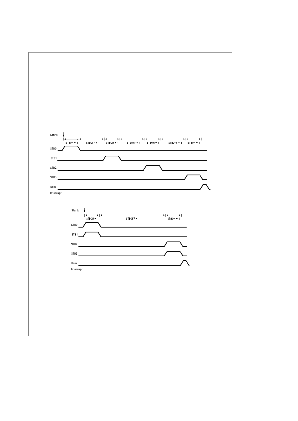
2.0 Architecture (Continued)
Strobes Generator
A train of strobes consists of two or four strobes depending
on the strobes mode. The train of strobe pulses starts on
the time slot pre-defined in the Printer Strobes-Start Time
Slot (PSTSL) register. The train of strobe pulses starts with
a strobe-on interval, followed by a sequence of strobe-off
and strobe-on intervals. The duration of the strobe-on interval is controlled by the STBON register and the duration of
the strobe-off interval is controlled by the STBOFF register.
The strobe-on and strobe-off intervals may be programmed
while the strobe pulses are being generated. After the last
strobe-on interval is completed, a Strobes-Done interrupt
pulse is generated. The interrupt is periodic, occurring when
the pre-defined time slot is reached and the train of strobe
pulses is completed.
Strobing pulses are generated on the STB0–3 output pins, if
enabled by the STBEN bit of the Thermal Print-Head Control (TPHC) register. After the last strobe-on interval is completed, the STBEN bit is automatically cleared by hardware.
To prevent losing strobe pulses, the software should verify
that the bit is cleared before setting it to ‘‘1’’.
The strobing mode defines both the number of strobes in a
train and the distribution of strobes among the STB0 –3
pins. Two strobing modes are supported, Two-Strobes
mode and Four-Strobes mode. The Strobe Mode (STBM)
field of the TPHC register selects the strobing mode to be
used.
The two strobing modes are shown in
Figure 2-12
and
Fig-
ure 2-13
for TPHC.SPOLe1. Note that ‘‘Start’’ is the begin-
ning of the time slot and ‘‘Done’’ is the Strobes-Done event.
TL/EE/11331– 17
FIGURE 2-12. Four Strobes Mode (STBMe00)
TL/EE/11331– 18
FIGURE 2-13. Two Strobes Mode (STBMe01)
26
Page 27
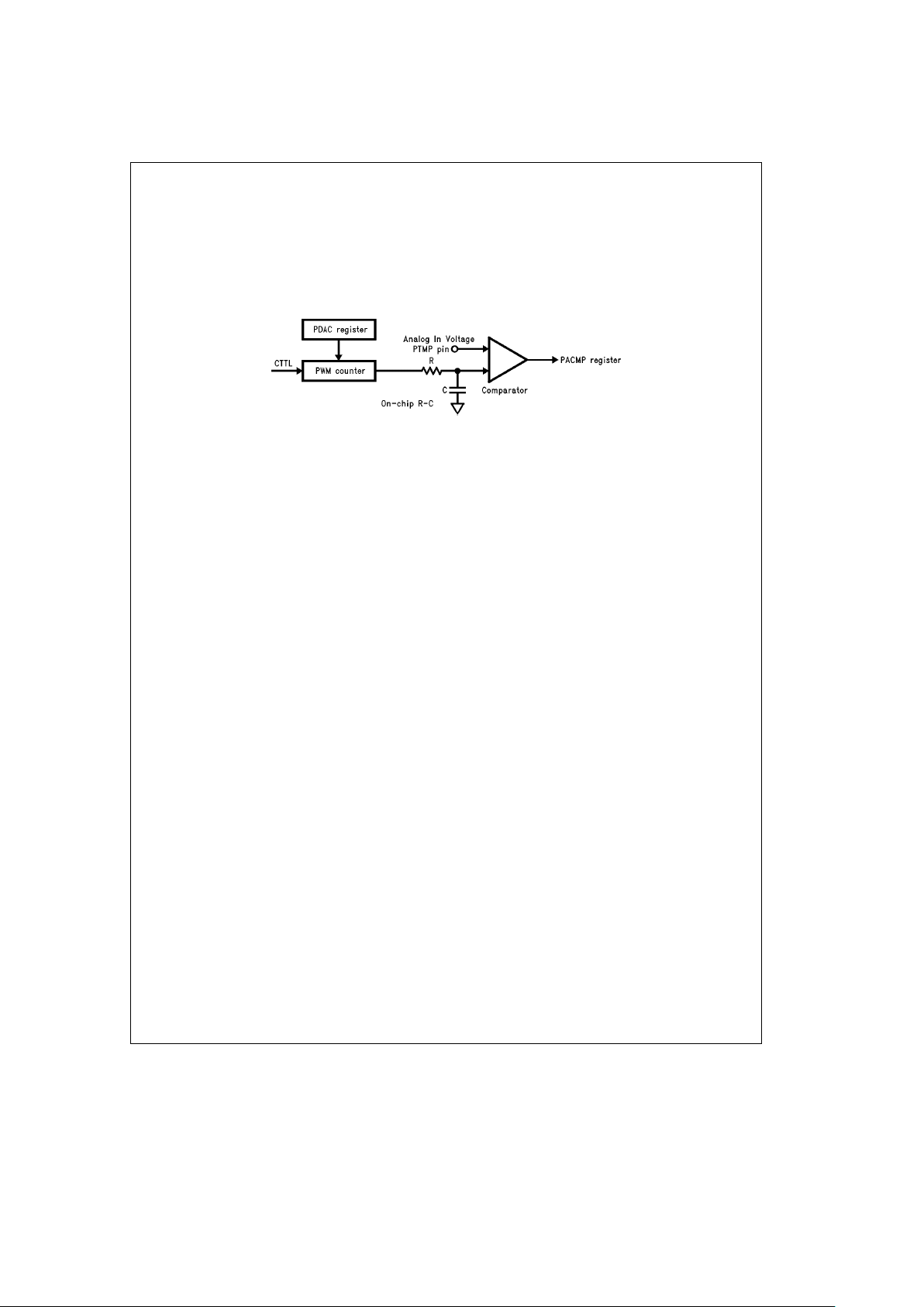
2.0 Architecture (Continued)
Printer Interrupt Generator
The Interrupt Control Unit dedicates one interrupt either to
the Strobes-Done pulse or to DMA channel 1. The Printer
Interrupt Source (PIS) bit of the TPHC register selects which
of the interrupt pulses is routed to the Interrupt Control Unit.
Temperature Sensing Circuit
A 6-bit A/D Converter (ADC) is implemented by a 6-bit
Pulse Width Modulation (PWM) based D/A convertor and
an analog comparator. The control loop of the ADC is executed under software control. The total time for both PWM
based D/A conversion and for comparator settling is less
than 2 ms. The DAC must be initialized to 011111 at least
10 ms prior to the first reading of the comparator output.
TL/EE/11331– 19
FIGURE 2-14. Temperature ADC
27
Page 28

2.0 Architecture (Continued)
2.5.3 Registers
PBCFG: Printer Bitmap Shifter Configuration register.
7210
res SLNR ECLK
ECLK: External Clock. (NS32FX200 only.)
0 : Shift using an internal clock. Clock frequency
is selected by the printer bitmap internal clock
generator.
1 : Shift using an external clock.
The external clock must be frozen at least
four instructions after both DMA channel 1
and the Bitmap Shifter are enabled (i.e.,
MCFG.EPBMS
e
1).
Note: Only the NS32FX200 supports operation using an
external clock. ECLK must always be cleared to
‘‘0’’ in the NS32FX100 and NS32FV100.
SLNR: Shift direction.
0 : Shift right (LSB first)
1 : Shift left (MSB first)
PBCFG may not be written while MCFG.ETPHB
e
1. It
should be configured before printer activation.
PCLON: Printer Bitmap Shifter internal clock (PCLK) high
time. 8-bit register.
PCLK is high for (PCLON
a
1) CTTL cycles.
PCLON may be modified only when
MCFG.EPBMS
e
0.
PCLOFF: Printer Bitmap Shifter internal clock (PCLK) low
time. 8-bit register.
PCLK is low for (PCLOFF
a
1) CTTL cycles.
PCLOFF may be modified only when
MCFG.EPBMS
e
0.
TPHC: Thermal Print-Head Control register.
7543210
res STBEN PIS SPOL STBM
STBM: Strobing mode (see
Figure 2-12
and
Figure
2-13
).
00 : Four strobes
01 : Two strobes
10 : Reserved
11 : Reserved
SPOL: Strobes polarity.
0 : Active low strobe-on
1 : Active high strobe-on
PIS: Printer Interrupt Source.
0 : Strobes done interrupt pulse
1 : DMA channel 1 interrupt pulse
STBEN: Strobes Enable.
Set by software to enable strobe generation on
strobe pins STB0–3. Automatically cleared by
hardware after the last strobe-on interval is completed. To avoid losing strobe pulses, verify that
this bit is cleared before setting it to ‘‘1’.
Upon reset the non-reserved bits of TPHC are cleared to
‘‘0’’.
STBON: Strobe-On. 16-bit register.
The strobe-on interval is (STBON
a
1) MCLK
cycles.
STBOFF: Strobe-Off. 16-bit register.
The strobe-off interval is (STBOFF
a
1) MCLK
cycles.
PSTSL: Printer Strobes Start Time Slot. 8-bit register.
Holds the time slot in which the strobe pulse train
starts.
PMTSL: Printer Motor Time-Slot. 8-bit register.
Holds the time slot in which the Printer Motor Interrupt Pulse is generated. The interrupt pulse occurs at the beginning of the specified time slot.
Note: For an event to occur at the beginning of time slot n, the
relevant register (PSTSL or PMTSL) must be set to the
value n
a
1. If the written value equals the TSL value
the current time slot) then the event will occur either in
the next time slot, or after 257 time slots.
Example: If a printer interrupt is to occur at the beginning of time slot
Ý
255 write the value ‘‘0’’ to PSTSL.
PDAC: Printer PWM Pulse Width Modulation DAC.
765 0
res PDAC
The PWM signal duty cycle is (PDACa1)/64.
The signal width is zero when PDACe3F.
PACMP: Printer Analog Comparator Status. 8-bit register.
Read only.
Bit 0:
1 : DAC voltage
l
PTMP pin voltage.
0 : DAC voltagekPTMP pin voltage.
Bits 1–7: Reserved.
2.5.4 Usage Recommendations
1. Before activating the Printer, program the appropriate
Ports module registers PBDO, PBMS, PCDO, PCMS and
PCEN to connect the Printer module to the NS32FX100
I/O pins.
2. Completion of the Printer Bitmap Shifter operation is indicated either through the STROBE-DONE interrupt or
through the DMA COUNTER-DONE status bit (STAT.TC
is set to ‘‘1’’). If indicated by the DMA STAT.TC bit, 32
additional bits must be explicitly shifted out of the Bitmap
Shifter, to complete the DMA transfer.
3. When TPHC.STBEN
e
0, strobes are still generated internally, hence the Strobes-done interrupt can still be
used even when strobes are disabled.
4. When using the Bitmap Shifter with an external clock the
operation must be carried out in the following order:
a. Initialize the ports module to work with the printer us-
ing an external clock (ports B and C).
5. Disable the strobes (TPHC.STBEN
e
0) before disabling
the TPH module (MCFG.ETPHB
e
0).
28
Page 29

2.0 Architecture (Continued)
b. Initialize the PRNTC module to work with an external
clock.
c. Initialize DMA channel 1 registers without enabling the
channel (set CNTL1.CHEN
e
0).
d. Set MCFG.ECOUNT, and MCFG.EPBMS to ‘‘1’’ to en-
able the PRNTC module.
e. Set CNTL1.CHEN to ‘‘1’’ to enable DMA channel 1.
f. Issue at least four instructions (may be NOPs).
g. Enable the external clock operation.
2.6 DIRECT MEMORY ACCESS CONTROLLER (DMAC)
2.6.1 Features
#
Four independent channels in NS32FX200, three in
NS32FX100 and NS32FV100
#
Single and double buffering, and auto-initialize modes
#
Fly-By or memory-to-I/O transactions
#
8- or 16-bit wide transactions
#
Maximum throughput 12.5 Mbyte/second
#
Channels configurable as internal or external
2.6.2 Description
The DMA Controller (DMAC) provides independent channels for transferring blocks of data between memory and
I/O devices with minimal CPU intervention. A block transfer
is composed of several byte or word transfers.
A general DMA channel, with eight registers and a superset
of features, is described first. Any on-chip DMA channel is
either similar to, or a subset of, this general channel. The
four NS32FX200 DMA channels, and the three NS32FX100
and NS32FV100 DMA channels, are described after the description of the general DMA channel.
2.6.2.1 A General DMA Channel
Memory address, block size and type of operation are set
up prior to DMA activation by programming the appropriate
control registers. Actual byte or word transfers are handled
by the DMA channel in response to I/O device requests.
Upon receiving a transfer request from an I/O device, the
DMA Controller performs the following operations:
1. Acquires control of the bus (via HOLD
, HLDA mecha-
nism).
2. Acknowledges the requesting I/O device, or one of several requesting I/O devices, according to the priority and
to the values stored in the control registers of the respective channel.
3. Executes the data transfer.
4. Updates the termination status bit (TC bit of the STAT
register) when the specified number of bytes has been
transferred.
2.6.2.2 Transfer Types
Each byte or word transfer can be carried out as one of the
following two types:
Fly-By (Direct) Transfers
In Fly-by mode each data item is transferred using a single
bus cycle without reading the data into the DMA Controller.
This mode offers the fastest transfer rate. Data transfer cannot occur between two memory elements. One of the elements must be the I/O device that requested the DMA
transfer. This device is referred to as the implied I/O device.
The other element can be either memory or another I/O
device, and is referred to as the addressed device. The
number of bytes transferred in each cycle is always two. Flyby DMA transactions are word aligned; device address and
block length must be even numbers. DMA transfers are controlled by the DMA module registers. A detailed description
of the DMA operation is provided in Section 2.6.3.
Memory-to-I/O (Indirect) Transfers
In Memory-to-I/O mode each data item is transferred using
two bus-cycles. Data transfer cannot occur between two
memory elements. One of the elements must be the I/O
device which requested the DMA transaction. This device is
referred to as the implied I/O device and is 8-bits wide. The
other element can be either memory or another I/O device,
is referred to as the addressed I/O device and is 16-bits
wide. The DMA controller takes care of both byte gathering
and scattering. DMA transfers are controlled by the DMA
module registers. A detailed description of the DMA operation is provided in Section 2.6.3. Memory-to-I/O transfers
are available only through channel 3.
2.6.2.3 Operation Modes
Each block transfer can be carried out in one of three
modes:
#
Single Buffer
Mode provides the simplest way to accomplish a
single block transfer operation. It performs
one DMA block transfer, and, when the
transfer is completed, prepares the specifications for the next transfer.
#
Double Buffer
Mode allows the software to set up the next
block-transfer specification while the current block-transfer is in progress.
#
Auto-Initialize
Mode allows the DMA Controller to continuously
fill the same memory area without software intervention.
A detailed description of the various modes of operation is
provided in Section 2.6.3.
2.6.3 Detailed Operation Flow
The DMA operation is controlled through the DMA registers.
The flow of the various DMA operations, using different registers for each transfer type and operation mode, is detailed
below:
Fly-By Operation
The address for the Fly-by mode is taken from the ADCA
counter register. The DMA channel generates either a read
or a write bus cycle according to the setting of the transfer
direction (DIR) bit in the MODE register. When the DIR bit is
‘‘0’’, a read bus-cycle from the addressed device is performed and the data is written to the implied I/O device.
When the DIR bit is ‘‘1’’, a write bus-cycle to the addressed
cycle is performed, and the data is read from the implied I/O
device. After the two bytes have been transferred, the Block
Length Counter (BLTC) is decremented by two. The Device
Address Counter (ADCA) is incremented or decremented by
two, or remains unchanged, according to the Decrement/Increment (DEC) and Device Address Control (ADA) bits in
the MODE register.
29
Page 30

2.0 Architecture (Continued)
Memory-to-I/O Operation
The data is first read from the source into the DMA Controller, and is subsequently written to the destination. When the
DIR bit is ‘‘0’’, the first bus-cycle is used to read data from
the addressed device according to the ADCA counter, while
the second bus-cycle is used to write the data into the implied I/O device according to the Implied I/O Device
(ADRB) register. When the DIR bit is ‘‘1’’, the first bus-cycle
is used to read data from the implied I/O device using the
ADRB register, while the second bus-cycle is used to write
the data into the addressed device according the ADCA
counter. The number of bytes transferred in each cycle is
always one. After the byte has been transferred, the BLTC
counter is decremented by one. The ADCA counter is incremented or decremented by one, or remains unchanged, according to the DEC and ADA bits in the MODE register.
ADRB is not changed.
Single Buffer Mode Operation
The block-transfer addresses and byte count should be first
written into the corresponding ADCA and BLTC counters
and the ADRB register. The Operator Type (OT) bit in the
MODE register should be programmed for non auto-initialize
mode, and the next Transfer Parameter Valid (VLD) bit in
the CNTL register should be cleared to ‘‘0’’. When the
Channel Enabled (CHEN) bit in the CNTL register is set to
‘‘1’’, the channel becomes active and responds to the transfer requests. When the BLTC counter reaches 0, the transfer operation terminates. The TC and Channel Overrun
(OVR) bits in the STAT register are set to ‘‘1’’ and Channel
Active (CHAC) is cleared to ‘‘0’’. If enabled through the ETC
bit, a Terminal Count (TC) interrupt pulse is generated. If the
EOVR bit in the STAT register is ‘‘1’’, the CHEN bit in the
CNTL register is forced to ‘‘0’’.
Double Buffer Mode Operation
The operation is initiated by writing the block-transfer address and byte count into the ADCA and BLTC counters and
ADRB register, then programming the OT bit in the MODE
register for non auto-initialize mode. When the CHEN bit in
the CNTL register is set to ‘‘1’’, the channel becomes active
and responds to transfer requests. While the current blocktransfer is in progress, the software can write the address
and byte count for the next block into the ADRA and BLTR
registers, respectively, and then set the VLD bit in the CNTL
register to ‘‘1’’. When the BLTC counter reaches 0, a TC
interrupt pulse is generated, if enabled, through the ETC bit.
The TC bit is set to ‘‘1’’ and the DMA channel checks the
value of the VLD bit. If it is ‘‘1’’, the channel copies ADRA
and BLTR values into ADCA and BLTC, respectively, clears
the VLD bit and starts the next block transfer. If the VLD bit
is ‘‘0’’, the channel sets the OVR bit in the STAT register to
‘‘1’’, clears the CHAC bit and, if the EOVR bit in the STAT
register is ‘‘1’’, it forces the CHEN bit to ‘‘0’’.
Auto Initialize Mode Operation
The operation is initialized by writing the block address and
byte count values into the ADCA and BLTC counters and
into the ADRA, ADRB and BLTR registers, and programming the OT bit in the MODE register for auto-initialize
mode. When the CHEN bit in the CNTR register is set to
‘‘1’’, the channel becomes active and responds to DMA re-
quests. When the BLTC counter reaches 0, a TC interrupt
pulse is generated, if enabled, through the ETC bit. The TC
bit in the STAT register is set to ‘‘1’’ and the contents of the
ADRA and BLTR registers are copied to the ADCA and
BLTC counters, respectively. The operation is repeated.
2.6.4 NS32FX200 DMA Channels
This section refers to the NS32FX200 since it has four DMA
channels, while the NS32FX100 and NS32FV100 have only
three. All references to channels 0 –2 are applicable to all
chips. All references to channel 3 are applicable to the
NS32FX200 only.
Channel 0 is for the scanner reference line fetches (write to
SVDB).
Channel 1 is for the printer bitmap fetches.
Channel 2 is for the scanner digitized-video writes.
Channel 3 is for external use.
Each of these three channels may be used as a general
purpose external DMA channel instead of the above mentioned use. This is done by the MCFG register. An external
DMA channel is accessible externally, via the Ports module.
Both MCFG bits and Port’s MS bits must be configured to
enable these DMA channels.
All the channels include STAT, ADCA, BLTC, MODE and
CNTL registers. Channels 1 and 3 support double buffer
operations, and include ADRA and BLTR registers. Channels 0 – 2 support only Fly-By (Direct) DMA transactions.
Channel 3 supports both Memory-to-I/O and Fly-By DMA
transactions and, therefore, includes an ADRB register.
Channel 0 has the highest priority, followed by channel 1,
channel 2, and, with lowest priority, channel 3. Refresh has
higher priority than DMA and it may occur between the two
bus transactions of a non fly-by DMA transaction. Priority is
resolved when the bus is idle, or on the last T3 of both CPU
and DMA transactions.
2.6.5 Registers
A DMA channel contains a set of eight registers. These registers are listed by their generic names. The DMA channel
number should be added as a suffix to the register name
when referring to a specific channel register (e.g., ADCA0,
ADCA1).
The registers ADCA, BLTC, STAT and MODE must be set
before activating the appropriate channel. Undefined results
are obtained when these registers are written while the
channel is enabled. Upon reset STAT and CNTL are cleared
to ‘‘0’’.
MODE Mode Control register. This register is used to
specify the channel operating mode.
15 1098 43210
res ADA res DIR NFBY DEC OT
OT Operation Type, for channels 1, 3 only (for chan-
nels 0, 2: reserved).
0 : Auto-Initialize mode disabled
1 : Auto-Initialize mode enabled
30
Page 31

2.0 Architecture (Continued)
DEC Decrement/Increment update of ADCA.
0 : ADCA incremented after each transfer cycle (if
ADA
e
1).
1 : ADCA decremented after each transfer cycle (if
ADA
e
1).
NFBY Fly-By/Memory-to-I/O Transfers, for channel 3
only (for channels 0, 1, 2: reserved).
0 : Fly-By
1 : Memory-to-I/O
DIR Transfer Direction.
Specifies the direction of the transfer between
memory and implied I/O device.
0 : Implied I/O Device is Destination
1 : Implied I/O Device is Source
ADA Device Address Control. Controls the update of the
ADCA counter after each transfer cycle.
0 : ADCA address unchanged
1 : ADCA address updated
ADCA Device Address Counter. 32-bit register.
Bits 0–23 : Hold the current address of either the
source data item or the destination location in the Addressed Device.
Bits 24–31 : Reserved.
If the ADA bit in the MODE register is
set to ‘‘1’’, ADCA is updated, according to DEC and FBY bits in MODE register, after every DMA transfer.
ADRA Device Address Register. 32-bit register. (Channels
1 and 3 only)
Bits 0–23 : Hold the starting address of the next
block to be transferred of either the
source data block or the destination
data area of the Addressed Device.
Bits 24–31 : Reserved.
ADRB Implied I/O Device register. 32-bit register. (Chan-
nel 3 only)
Bits 0–23 : Hold the address of either the source
data block or the destination data
area of the implied I/O device.
Bits 24–31 : Reserved.
BLTC Block Length Counter. 32-bit register.
Bits 0–23 : Hold the current number of bytes to
be transferred.
Bits 24–31 : Reserved.
BLTC is decremented, after each transfer, according to FBY bit in MODE register.
BLTR Block Length Register. 32-bit register. (Channels 1
and 3 only)
Bits 0–23 : Hold the number of bytes in the next
block to be transferred.
Bits 24–31 : Reserved.
A ‘‘0’’ value in the BLTR register, while the VLD
and CHEN in the CNTL register are both set to ‘‘1’’,
may cause unpredictable results.
STAT Status register. This register has two functions:
Holds status information for the DMA channel.
Used to enable or mask the DMA interrupts for the
various terminations conditions.
76543210
Res EOVR res ETC CHAC OVR res TC
TC Terminal Count.
When set to ‘‘1’’ indicates that the transfer was
completed by a terminal count condition (BLTC)
reached 0).
OVR Channel Overrun. (Channels 1, 3 only)
Set to ‘‘1’’, in non auto-initialize mode, when the
present transfer is completed (BLTC
e
0), but the
parameters for the next transfer are not valid (VLD
bit in CNTL is ‘‘0’’).
CHAC Channel Active. Read Only.
When set to ‘‘1’’, indicates that the channel is active (CHEN bit in CNTL register is ‘‘1’’ and BLTC
l
0).
This bit continuously reflects the active or inactive
status of the channel, and therefore, can only be
read. Data written to the CHAC bit is ignored.
ETC Enables interrupt pulse when the BLTC counter
reaches 0.
0 : Disable
1 : Enable
EOVR Enables interrupt pulse when OVR bit is set. (Chan-
nels 1, 3 only)
0 : Disable
1 : Enable
The TC and OVR bits are sticky. This means that once set
by the occurrence of the specific condition, they will remain
set until explicitly cleared by software. Those bits can be
individually cleared by writing a value into the STAT register
with the bit positions to be cleared set to ‘‘1’’. Writing ‘‘0’’ to
those bits has no effect.
CNTL Control register.
This register is used to synchronize the channel
operation with the programming of the block transfer parameters.
7210
res VLD CHEN
CHEN Channel Enable.
0 : Channel Disable
1 : Channel Enable
The CHEN bit is cleared to ‘‘0’’ in the following
cases.
(1) Upon Reset
(2) Software clears it by writing to the CNTL regis-
ter.
31
Page 32

2.0 Architecture (Continued)
(3) The OVR bit in the STAT register is set to ‘‘1’’
and the EOVR bit is ‘‘1’’. In the last case the
CHEN bit is forced to ‘‘0’’ and cannot be set to
‘‘1’’ by software unless the OVR is either
cleared or masked by clearing the EOVR bit in
the STAT register.
VLD Transfer Parameter Valid. Indicates whether the
transfer parameters for the next block to be transferred are valid. The VLD bit is ignored in auto-initialize operation mode and is cleared by hardware
after ADRA and BLTR have been copied to ADCA
and BLTC respectively. VLD is used to distinguish
between single transfer and double-buffer operation modes.
2.6.6 Usage Recommendations
1. Before activating the DMA, program the appropriate
Ports module registers PBDO, PBMS, PCDO, PCMS and
PCEN to connect the DMA to the NS32FX100 I/O pins.
2. Set the MCFG register to allocate the DMA channels as
either internal or external, as appropriate.
3. The Ports module must be configured to allow the allocation of the I/O pins to the DMA channels.
2.6.7 DMAC Bus Cycles
TL/EE/11331– 20
FIGURE 2-15. DMA Fly-By Read Transaction (DIRe0, NFBYe0)
The maximum throughput of a DMA channel is 12.5 Mbyte/sec. (Two bytes can be transferred at a rate of four CTTL cycles per
transfer, up to 25 MHz.)
Note 1: Memory control signals (like CWAIT, select and write enable) are generated according to the specifications of the accessed zone.
Note 2: A
v
in the figure indicates DMA priority resolving points.
32
Page 33

2.0 Architecture (Continued)
TL/EE/11331– 21
FIGURE 2-16. DMA Fly-By Write Transaction (DIRe1, NFBYe0)
The maximum throughput of a DMA channel is 12.5 Mbyte/sec. (Two bytes can be transferred at a rate of four CTTL cycles per
transfer, up to 25 MHz.)
Note 1: Memory control signals (like CWAIT, select and write enable) are generated according to the specifications of the accessed zone.
Note 2: The NS32FX100 does not drive data onto AD0– 15 till the end of T4 in memory
Ý
I/O transactions (like NS32FX100 register read transactions).
Note 3: A
v
in the figure indicates DMA priority resolving points.
33
Page 34

2.0 Architecture (Continued)
TL/EE/11331– 22
FIGURE 2-17. DMA Memory to I/O (Indirect) Read Transaction (DIRe0, NFBYe1)
The maximum throughput of a DMA channel is 3.125 Mbyte/sec. (One byte can be transferred at a rate of eight CTTL cycles per
transfer, up to 25 MHz.)
Note 1: Memory control signals (like CWAIT, select and write enable) are generated according to the specifications of the accessed zone.
Note 2: The NS32FX100 does not drive data onto AD0– 15 till the end of T4 in memory
Ý
I/O transactions (like NS32FX100 register read transactions).
Note 3: A
v
in the figure indicates DMA priority resolving points.
34
Page 35

2.0 Architecture (Continued)
TL/EE/11331– 23
FIGURE 2-18. DMA I/O to Memory Write Transaction (DIRe1, NFBYe1)
The maximum throughput of a DMA channel is 3.125 Mbyte/sec. (One byte can be transferred at a rate of eight CTTL cycles per
transfer, up to 25 MHz.)
Note 1: Memory control signals (like CWAIT, select and write enable) are generated according to the specifications of the accessed zone.
Note 2: The NS32FX100 does not drive data onto AD0– 15 till the end of T4 in memory
Ý
I/O transactions (like NS32FX100 register read transactions).
Note 3: A
v
in the figure indicates DMA priority resolving points.
35
Page 36

2.0 Architecture (Continued)
TL/EE/11331– 24
FIGURE 2-19. Two Adjacent Fly-By DMA Transactions
The maximum throughput of a DMA channel is 12.5 Mbyte/sec. (Two bytes can be transferred at a rate of four CTTL cycles per
transfer, up to 25 MHz.)
Note 1: Memory control signals (like CWAIT, select and write enable) are generated according to the specifications of the accessed zone.
Note 2: A
v
in the figure indicates DMA priority resolving points.
2.7 UNIVERSAL ASYNCHRONOUS RECEIVERTRANSMITTER (UART)
2.7.1 Features
Y
Full duplex double-buffered transmitter/receiver
Y
Programmable baud rate between 300 and CTTL/32
baud
Y
Hardware flow control
Y
Asynchronous 7-bit or 8-bit character transmission/
reception
Y
Supports transmission of one or two stop bits
Y
Hardware support of odd or even parity-bit generation
during transmission
Y
Hardware support of odd or even parity check during
reception
Y
Maskable interrupt on transmit ready or receive ready,
regardless of reception errors
Y
Data sampled at 16 times the baud rate
Y
Software-controlled break transmission and detection
2.7.2 Operation
The Universal Asynchronous Receiver Transmitter (UART)
module enables the NS32FX100 to communicate with standard serial devices using three communication signals:
transmit, receive and ground. A character is composed of a
start bit followed by data bits (the least significant bit right
after the start bit) followed by an optional parity bit and at
least one stop bit. The communication is serialÐthe transmit and receive signals hold one bit at a time. Bit duration is
one baud time.
The UART can be configured with the following communication parameters: 7-bit or 8-bit data formats, with or without
parity, with one or two stop bits.
Baud rate is generated internally, by dividing CTTL under
software control. Break is generated under software control.
Break detection is via the frame error status bit (UCLST.FE).
The UART is full-duplex, it can transmit and receive characters simultaneously. The software may use either polling or
interrupts to operate the UART. Both transmission and reception are double buffered to relax software response
time.
36
Page 37

2.0 Architecture (Continued)
A transmit interrupt is generated on transmit ready, if not
masked by the UMASK register. A receive interrupt is generated, if not masked by the UMASK register, on receive
ready for every received character regardless of the occurrence of a reception error. A reception error has no effect
on the current or the next data reception. i.e., the current
data is available in the data buffer and the next data reception will occur in the usual way.
No reception is enabled during break on the UART Receive
(URXD) pin. A high-to-low transition is, therefore, required to
detect a start bit.
The UART data buffers are eight bits wide.
Whenever a new character is received, and the data buffer
is empty, the data buffer and the status register are updated. Hardware flow control can be implemented either by
software (using the Ports module) or by hardware. When
controlled by hardware, transmission starts only if the
Transmit Enable input pin (UTEN
) is asserted low. Once a
byte transmission starts, the UTEN
value is ignored till the
stop bit is transmitted.
The Receive Enable output pin (UREN
) is inactive (high)
when both the receiver shifter and buffer are full. UREN
is
asserted low when the buffer or the shifter is empty.
2.7.3 Registers
URXB: Reception data buffer. Read only. 8-bit register.
Bit 0 is the first bit serially received.
Bit 7 is cleared during reception of 7-bit characters.
Reading URXB updates the UCLST.RF status bit.
If a new character is ready in the shifter, the
URXB is updated with the new value after the
current value has been read.
UTXB: Transmission data buffer. 8-bit register.
Bit 0 is the first bit serially transmitted.
Bit 7 is ignored during transmission of 7-bit characters.
UBRGL: Low byte of the CTTL clock divider (UBRG). 8-bit
register.
UBRGH: High byte of the CTTL clock divider (UBRG). 8-bit
register.
These two, one-byte, registers are used to generate a clock, whose frequency is 16 times the
baud rate, according to the following equation:
CTTL/(UBRG
a1)e
baud-rate * 16.
UCNTL: UART Control register.
Controls the number of data and stop bits, parity
enable/disable and odd/even and break transmission on/off. Upon reset all the non reserved
bits are cleared to ‘‘0’’.
UMASK: UART Mask Interrupts register. Upon reset, the
implemented bits are cleared to ‘‘0’’.
7210
res MTI MRI
MTI: Mask Transmit Interrupt
0: Transmit Interrupt is not masked
1: Transmit Interrupt is masked
MTI: Mask Receive Interrupt
0: Receive Interrupt is not masked
1: Receive Interrupt is masked
TL/EE/11331– 25
FIGURE 2-20. Character Format
37
Page 38

2.0 Architecture (Continued)
7654321 0
TBRK res res res TSB EDB PEN EPS
EPS: Even Parity Select.
0 : Odd parity
1 : Even parity
Even parity means that the total number of bits
set (including the parity bit) is even.
PEN: Parity Enable.
0 : Parity disabled
1 : Parity enabled
EDB: Number of data bits.
0 : Seven data bits
1 : Eight data bits
TSB: Number of stop bits transmitted.
0 : One stop bit
1 : Two stop bits
TBRK: Transmission Break ControlÐimplemented by
forcing UTXD pin low.
0 : No break signal
1 : Break signal
Undefined results when TBRK is ‘‘1’’ while
UCLST.TE is ‘‘0’’.
UCLST: UART Clearing Status register. 8-bit register.
76543210
TR TE res OE res FE PE RF
Receive status bits: Upon reset, these status bits are
cleared to ‘‘0’’.
RF: Receive Full. RF
e
1 when URXB is loaded by the
shift register.
PE: Parity Error. PE
e
1 when parity error is detected.
FE: Frame Error. FEe1 when the first stop bit is ‘‘0’’.
OE: Overrun Error. OEe1 when both reception buffer and
shifter are full and a new character is received.
Transmit status bits: Upon reset, these status bits are set to
‘‘1’’.
TE: Transmit Empty. TE
e
1 when both UTXB and the
shifter are empty.
TR: Transmit Ready. TR
e
1 when UTXB is empty.
OE status bit is sticky. Once set, it is cleared by reset or by
writing into UCLST (data written into this register is ignored).
RF is cleared during reset. It is set to ‘‘1’’ when URXB is
loaded by the shift register. It is updated by a URXB read:
RF remains ‘‘1’’ if the shifter already holds a new character,
and is cleared to ‘‘0’’ if the shifter did not finish reception of
a new character.
PE and FE bits are sticky. These two bits are cleared during
reset and whenever UCLST is read.
2.7.4 Usage Recommendations
1. Before activating the UART, program the appropriate
Ports module registers PADI, PAMS, PBDO, PBMS,
PCDO, PCMS and PCEN to connect the UART module
to the NS32FX100 I/O pins.
2. Initialization:
a. Disable interrupts or mask the UART interrupt.
b. Initialize UBRG and then UCNTL.
c. Clear receiver status bits using URXB and UCLST.
d. Enable UART interrupt, if required.
e. Program the PAMS register in the Ports module as
follows:
MS0 must be cleared before data is transmitted from the UART.
MS1 must be set before data can be received on the URXT pin.
3. To use the PE and FE status bits as non-sticky bits, read
the UCLST before reading URXB. Note that right after
URXB is read, it might be loaded with a new character
which was waiting in the shifter, and those status bits
might be set by the new URXB. Therefore, it is recommended to read UCLST first and then read URXB, thus
keeping coherence between the contents of URXB and
UCLST.
4. When UTEN
is inactive, the TE bit does not ensure that
two characters may be written to the UTXB. The TR bit
must be ‘‘0’’ before each UTXB write.
2.8 MICROWIRE (MWIRE)
2.8.1 Features
Y
Operates as a MICROWIRE master
Y
Programmable shift-clock frequency
Y
8-bit serial I/O data shift register
Y
Busy flag for polling and as an interrupt source
Y
Two modes of clocking data
2.8.2 Operation
The MICROWIRE (MWIRE) is a serial synchronous communication interface. It enables an interface with any National
Semiconductor chip that supports MICROWIRE protocol,
such as COPs and EEPROMs. The MWIRE interface consists of three signals: serial data in, serial data out, and
serial clock. Several devices may share the same MWIRE
channel by means of device-select signals. Such select signals may be provided by the Ports module. The MWIRE
outputs may be TRI-STATED by the Ports module. A high
level interrupt is generated when the MWIRE is not busy,
and is cleared only while MWIRE is busy. The serial data is
sampled on the serial clock falling edge. The serial data out
may change on the serial clock rising or falling edge, according to the software selected mode.
2.8.3 Registers
MWSIO: MICROWIRE Serial I/O Shift register. 8-bit shift
register.
Used for data transfer over the MWIRE channel.
Bit-7, the most significant bit, is transmitted first.
38
Page 39

2.0 Architecture (Continued)
Accessing MWSIO while the MWIRE is busy
(MWCSR.BUSY
e
1) may cause unpredictable
results.
MWCSR: MICROWIRE Control and Status register.
754310
res CLKM CDV BUSY
BUSY: Read only. Set to ‘‘1’’ during MWIRE transaction.
Cleared to ‘‘0’’ on termination. Used also as the
MICROWIRE interrupt source.
CDV: Clock Divider.
Divides the MCLK clock by 2**n, where n
e
[
0..5], to generate the MWIRE shift clock.
000 : Non divided MCLK
001 : MCLK/2
010 : MCLK/4
011 : MCLK/8
100 : MCLK/16
101 : MCLK/32
Other : Reserved
CLKM: Clocking mode:
0 : MWSO changed on MWSK rising edge.
MWSK clock is high when MWIRE is idle.
1 : MWSO changed on MWSK falling edge.
MWSK clock is low when MWIRE is idle.
TL/EE/11331– 26
FIGURE 2-21. MICROWIRE Transaction (CLKMe0)
TL/EE/11331– 27
FIGURE 2-22. MICROWIRE Transaction (CLKMe1)
39
Page 40

2.0 Architecture (Continued)
2.8.4 Usage Recommendations
1. Before activating the MICROWIRE, program the appropriate Ports module registers PBDO, PBMS, PCDO,
PCMS and PCEN to connect the MICROWIRE module to
the NS32FX100 I/O pins.
2. The correct sequence for a MWIRE transaction is to select a device, issue the MWIRE transaction, and then deselect the device. A device can be selected either by
using the Ports module, or implicitly if only one device is
connected to the bus).
3. Writing to MWSIO register triggers the shift transaction.
Reading the MWSIO does not trigger a shift transaction
but returns the current contents of the MWSIO. For a
read transaction, perform a dummy write transaction to
initiate the shift and then read the MWSIO, i.e., write a
byte, wait until not busy and then read the result.
2.9 INTERRUPT CONTROL UNIT (ICU)
2.9.1 Features
Y
16 interrupt sources
Y
Supports CPU vectored-interrupt mode
Y
Fixed priority among interrupt sources
Y
Individual enable/disable of each interrupt source
Y
Polling support by an interrupt pending register
Y
Programmable triggering mode and polarity
2.9.2 Operation
The Interrupt Control Unit (ICU) receives interrupt signals
from internal and external sources and generates a vector
interrupt to the CPU when required. Priority among the interrupt sources if fixed. Each interrupt source can be individually enabled or disabled. Pending interrupts can be polled
using the interrupt pending register, regardless of their being
enabled or disabled.
The ICU triggering mode and polarity of each interrupt
source (individually) are both programmed via the Interrupt
Edge/Level Trigger register (IELTG) and the Interrupt Trigger Polarity register (ITRPL). Both the polarity and the triggering mode of the interrupts that are generated on-chip are
fixed. It is the software’s responsibility to program the respective bits in IELTG and ITRPL as required.
Edge-triggered interrupts are latched by the interrupt pending register. A pending edge-triggered interrupt is cleared by
writing the required value to the edge interrupt clear register. A pending level-triggered interrupt is cleared only when
the interrupt source is not active.
Interrupt vector numbers are always positive, in the range
20(hex) to 2F(hex).
MCFG.ESCAN bit controls the IRQ11 interrupt source.
MCFG.EDMA0 bit controls the IRQ13 interrupt source.
TPHC.PIS bit controls the IRQ14 interrupt source.
The external interrupt inputs are asynchronous. They are
recognized by the NS32FX100 during cycles in which the
input setup and hold time requirements are satisfied.
TABLE 2-3. Interrupt Sources and Priority Levels
IRQ0 Internal Level-High MICROWIRE Lowest Priority
IRQ1 External INT0 Pin
IRQ2 Internal Edge-Rising System Tick
IRQ3 Internal Edge-Rising TIMER Pulse
IRQ4 External INT1 Pin
IRQ5 Internal Level-High UART
IRQ6 Internal Level-High SDC Transmit
IRQ7 Internal Level-High SDC Receive
IRQ8 Internal Level-High SDC Error
IRQ9 External INT2 Pin
IRQ10 Internal Edge-Rising Printer Motor
IRQ11 Internal Edge-Rising Scanner Motor or DMA Channel 2
(Selected by MCFG)
IRQ12 Internal Edge-Rising DMA Channel 3
IRQ13 Internal Edge-Rising Scanner or DMA Channel 0 (Selected by
MCFG)
IRQ14 Internal Edge-Rising Printer or DMA Channel 1 (Selected by
TPHC)
IRQ15 External INT3 Pin Highest Priority
40
Page 41

2.0 Architecture (Continued)
2.9.3 Registers
IVCT: Interrupt Vector register. Read only. 8-bit regis-
ter.
76543 0
0 0 1 0 INTVECT
INTVECT: When INTR pin is active, this field contains the
encoded value of the enabled pending interrupt
that has the highest priority.
IENAM: Interrupt Enable And Mask register. 16-bit regis-
ter.
Enables each interrupt individually.
The bits of IENAM correspond to interrupts 0–
15. Each bit is encoded as follows:
0 : Interrupt is disabled.
1 : Interrupt is enabled.
IPEND: Interrupt Pending register. Read only. 16-bit reg-
ister.
Indicates which interrupts are pending. Bits 0–
15 of IPND correspond to interrupts 0 –15. Each
bit is encoded as follows:
0 : Interrupt is not pending.
1 : Interrupt is pending.
IECLR: Edge Interrupt Clear register. Write only. 16-bit
register.
Used to clear pending, edge-triggered, interrupts. Writing to the bit positions of level-triggered interrupts has no effect. The bits of IECLR
correspond to interrupts 0 –15. Each bit is encoded as follows:
0 : No effect.
1 : Clear the pending interrupt.
IELTG: Edge/Level Trigger. 16-bit register.
Each bit defines the way that the corresponding
interrupt request is triggered, either edge-sensitive or level-sensitive.
Each IETLG bit is encoded as follows:
0 : Level-sensitive.
1 : Edge-sensitive.
For normal invocation of internal interrupt sources, bits 0, 5, 6, 7 and 8 must be ‘‘0’’; bits 2, 3, 10,
11, 12, 13 and 14 must be ‘‘1’’.
ITRPL: Trigger Polarity. ITRPL is a 16-bit register that
controls the triggering polarity. ITRPL bits are
encoded as follows:
Level-sensitive trigger type:
0 : Low level.
1 : High level.
Edge-sensitive trigger type:
0 : Falling edge.
1 : Rising edge.
For normal invocation of internal interrupt sources, bits 0, 2, 3, 5, 6, 7, 8, 10, 11, 12, 13 and 14
must be ‘‘1’’.
Program the IELTG and ITRPL registers, to control the ICU mode and polarity, as follows:
IELTG ITRPL Mode
0 0 Low Level
0 1 High Level
1 0 Falling Edge
1 1 Rising Edge
2.9.4 Usage Recommendations
1. Initialization:
The recommended initialization sequence is:
a. Initialize the INTBASE register of the CPU
b. Program the interrupts’ triggering mode and polarity
c. Prepare the interrupt routines of the used interrupts
d. Clear the used edge-interrupt
e. Set the relevant bits of IENAM
f. Enable the CPU interrupt (via the PSR register of the
CPU)
2. Clearing:
Clearing an interrupt request before it is serviced may
cause a spurious interrupt, (i.e., the CPU detects an interrupt not reflected by IVCT). The user is advised to clear
interrupt requests only when interrupts are disabled.
Changing triggering mode or polarity may also cause a
spurious interrupt and should thus be carried out only
when the interrupts are disabled.
Clearing any of the IENAM bits should be carried out
while the I bit in the PSR register of the CPU is cleared.
3. Nesting:
There is no hardware limitation on nesting of interrupts.
Interrupts’ nesting is controlled by writing into the Enable
And Mask register (IENAM). When the CPU acknowledges an interrupt, the CPU’s PSR.I bit is cleared to ‘‘0’’,
thus disabling interrupts. While an interrupt is in service,
the user may allow other interrupts to occur by updating
IENAM, then setting PSR.I bit to ‘‘1’’. The IENAM register
can be used to control which of the other interrupts is
enabled.
2.10 PORTS MODULE
2.10.1 Features
Y
Individual or group enable/set/clear of any output port
Y
Read latched state of input ports
Y
Some Port I/O pins can be allocated to other modules
Y
External extension output port support
2.10.2 Operation
This module includes three types of ports:
Ð General-purpose input/output ports.
Ð External output port extension.
Ð Stepper-motors output ports.
2.10.2.1 General Purpose Input/Output Ports
These ports enable access to individual, general-purpose,
input/output pins. There are three general purpose ports.
Port A provides four input pins, Port B provides 12 output
pins, Port C provides eight I/O pins. Some pins are shared
41
Page 42

2.0 Architecture (Continued)
with other modules, and are allocated by software. Input
pins can always be read, even if shared with another module. Output pins can be enabled or disabled (TRI-STATE).
The characteristics of the four bits which may be associated
with the ports are as follows:
Ð DI: Data In bit. Read only. Holds current value/state of
the pin.
Ð DO: Data Out bit. Write/read. Holds the value to be
driven onto the pin when the respective MS bit is
‘‘0’’. When read back, DO is not effected by the
MS bit.
Ð EN: Enable bit. Write/read. TRI-STATE when EN
e
0,
drive when EN
e
1.
Ð MS: Module Select bit. Write/read. Selects output pin
source and input pin destination.
When MS
e
0, pin is connected to the port.
When MSe1, pin is connected to the module
that shares this pin.
When an input signal is assigned to a module (by setting the
respective MS bit to ‘‘1’’), the associated EN bit must be
cleared to ‘‘0’’.
TL/EE/11331– 28
FIGURE 2-23. Port A
Two bits are associated with each input pin of this port:
DI: Data In Bit
MS: Module Select Bit
TL/EE/11331– 29
FIGURE 2-24. Port B
Three bits are associated with each output pin of this port:
DO: Data Out Bit
EN: Enable Bit
MS: Module Select Bit
TL/EE/11331– 30
FIGURE 2-25. Port C
42
Page 43

2.0 Architecture (Continued)
Four bits are associated with each general purpose I/O pin
of this port:
DI: Data In Bit
DO: Data Out Bit
EN: Enable Bit
MS: Module Select Bit
Port input data is asynchronous. When the input is read
while it is changing, the value read is unreliable. The software should read an input either when it is guaranteed that
the input is stable, or perform debouncing. If the input satisfies the required set-up and hold times, the value read is the
true input value. With the exception of URXD and UTEN
,
when an input is assigned to a module it must satisfy the
required set-up and hold times. The results are unpredictable if this requirement is not satisfied.
2.10.2.2 External Output Port Extension
The number of output ports of an NS32FX100-based FAX
system can be expanded by an external latch, such as the
DM74LS373 chip. Two such latches can add 16 output pins
without any additional glue logic. This module controls such
an external latch.
TL/EE/11331– 31
FIGURE 2-26. External Output Port Extension
The latch data inputs are taken from the system data bus.
The latching signal is generated by the NS32FX100. The
NS32FX100 includes the PEXT register, which is an on-chip
mirror register of the external latch. This is used to ease the
setting, or clearing, of individual bits by enabling the CPU to
read back the port value, modify the required bit(s) and write
the new value to the external latch. The read back is performed from PEXT rather than from the write-only external
latch. Writing is performed simultaneously to both the external latch and to PEXT. The external latching signal is generated when PEXT is being written into. i.e., at T3 of the write
transaction. It is also active during reset to enable initialization of the external output port extension.
2.10.2.3 Stepper Motors Output Ports
The stepper motor is controlled by four phases. The phases
values are stored by software into the Ports module registers and are transferred into the phase pins by the motor
interrupt pulse rising edge.
2.10.3 Registers
PADI: Port A data in. Read only.
Each bit holds the current value of the corresponding input pin.
7 43210
res DMRQ3 MWSI URXD UTEN
PAMS: Port A module select.
7210
res MS1 MS0
MS0, MS1: Module select bits for Port A input pins.
The UART’s UTEN input is forced low when
MS0
e
0.
The UART’s URXD input is forced high when
MS1
e
0.
res: Reserved
MS0 must be cleared before data is transmitted from the
UART.
MS1 must be set before data can be received on the
URXD pin.
Upon reset this register is cleared to ‘‘0’’.
PBDO: Port B data out.
Each bit holds the value driven onto the corresponding output pin when the respective MS bit, in
the PBMS register, is ‘‘0’’.
76543210
DMAK3
SDIS/
DMAK1
SCLK2/
STB3 STB2 STB1 STB0
DMAK2
DMAK0
15 12 11 10 9 8
res SLS SCLK1 SPDW MSWK
PBMS: Port B module select.
151211109876543210
res MS11 MS10 MS9 MS8 MS7 MS6 MS5 MS4 MS3 MS2 MS1 MS0
MS0–MS11: Module select bits for Port B output pins.
0 : Port is selected.
The value of the corresponding bit in the PBDO register is driven on the respective pin, when Port B is enabled through the PBEM register.
1 : Module is selected.
The value of the pin specified by the corresponding bit
in the PBDO register is driven from the appropriate
module: Printer, Scanner, DMA.
Upon reset this register is cleared to ‘‘0’’.
When the Scanner or the DMA module is activated through
the MCFG register, MS4 and MS6 must be set to ‘‘1’’ as
detailed in the following table:
Module MCFG.EDMA0 MS4 Module MCFG.ESCAN MS6
DMA 0 1 DMA 0 1
Scanner 1 1 Scanner 1 1
Port X 0 Port X 0
PBEN: Port B enable.
15 1 0
res EN
EN: Controls the pins’ state. All pins are driven when
this bit is set. Upon reset bit 0 is cleared, causing
the output pins to be in TRI-STATE.
43
Page 44

2.0 Architecture (Continued)
PCDI: Port C data in. Read only.
Holds the current value of the pins (latched once
each CTTL).
76 5 4 3 2 10
UREN UTXD MWSO
SBPYS/ PCLK/ SNH/
PIO1 PIO0
DMRQ2
DMRQ1 DMRQ0
PCDO: Port C data out.
Each bit holds the value driven onto the corresponding output pin when the respective MS bit, in
the PCMS, register is ‘‘0’’.
76543210
UREN UTXD MWSO
SBYPS/ PCLK/ SNH/
PIO1 PIO0
DMRQ2
DMRQ1 DMRQ0
PCMS: Port C module select.
76543210
MS7 MS6 MS5 MS4 MS3 MS2 res
MS2–MS7: The module select bits for port C I/O
pins.
0 : Port is selected.
The value of the corresponding bit in the PCDO
register is driven on the respective pin, when
Port C is enabled through the PCEN register.
1 : Module is selected.
The value of the pin specified by the corresponding bit in the PCDO register is driven to/
from the appropriate module: Printer, Scanner,
DMA.
Upon reset this register is cleared to ‘‘0’’.
When the Scanner, Printer or DMA module is activated
through the MCFG register, MS2, MS3 and MS4 must be set
to ‘‘1’’ as detailed in the following table.
Module MCFG.EDMA0 MS2 Module MCFG.EPBMS MS3 Module MCFG.ESCAN MS4
DMA 0 1 DMA 0 1 DMA 0 1
Scanner 1 1 Printer 1 1 Scanner 1 1
Port X 0 Port X 0 Port X 0
44
Page 45

2.0 Architecture (Continued)
PCEN: Port C Enable.
76543210
EN7 EN6 EN5 EN4 EN3 EN2 EN1 EN0
EN0–EN7: Enable bit for Port C output pins.
A pin is driven when its relevant ENi bit is set to
‘‘1’’, or not driven (TRI-STATE) when its relevant
ENi bit is cleared to ‘‘0’’.
The inputs are readable regardless of the state of
the respective ENi bit. Upon reset PCEN is cleared
to ‘‘0’’.
PEXT: External output port mirror register. 16-bit register.
When this register is read, no external latch pulse
is generated.
When this register is written, an external latch
pulse is generated to enable simultaneous write
into both this register and the external latch.
PMPH: Printer Motor Phase Register. 8-bit register.
The register holds the value to be driven by the
PMPH0–3 pins on the next printer motor interrupt
rising edge. Bits 0 – 3 control the four phases. Bits
4–7 are reserved.
A double buffer is used to latch the next values and
to drive the pins. The PMPH0–3 pins are always
driving.
Upon reset the pins are driven low.
SMPH: Scanner Motor Phase register. 8-bit register.
The register holds the value to be driven by the
SMPH0–3 pins on the next scanner motor interrupt
rising edge. Bits 0 – 3 control the four phases. Bits
4–7 are reserved.
A double buffer is used to latch the next values and
to drive the pins. The SMPH0 – 3 pins are always
driving.
Upon reset the pins are driven low.
2.10.4 Usage Recommendations
When working with the Printer Bitmap Shifter, using DMA
channel 1 to load the shifter, the PBMS.MS5 bit must be
cleared to ‘‘0’’ (PBMS.MS5
e
0).
2.11 BUS AND MEMORY CONTROLLER (BMC)
2.11.1 Features
Y
Direct interface to the CPU bus
Y
Direct interface with ROM, SRAM and I/O devices
Y
Programmable wait-state generator
Y
Supports both 8-bit and 16-bit access requests
Y
Direct interface with DRAM (NS32FX200 and
NS32FV100 only).
Y
CAS before RAS, DRAM refresh (NS32FX200 and
NS32FV100 only)
2.11.2 Operation
The Bus and Memory Controller (BMC) directly interfaces to
the CPU. It responds to read and write transactions and
generates DMA transactions. The memory controller directly interfaces to ROM, SRAM and I/O devices. The
NS32FX200 and NS32FV100 also support DRAM devices.
It generates the required memory control and CPU wait signals.
The BMC decodes the high-order address bits and distinguishes between five zones, one zone for access to the
NS32FX100 on-chip memory-mapped registers and four external zones. The wait-state generator inserts a programmable number of wait-states according to the accessed address zone.
Address decoding (Hex):
Address: 000000–3FFFFF Configurable
(4 Mbyte): Zone
Ý
0ÐROM or
Zone
Ý
2ÐDRAM.
(NS32FX100 always:
Zone
Ý
0ÐROM)
Address: 400000–7FFFFF ZoneÝ2ÐDRAM.
(4 Mbyte): (NS32FX100ÐReserved)
Address: 800000–BFFFFF Zone
Ý
0ÐROM.
(4 Mbyte):
Address: C00000–DFFFFF Zone
Ý
1ÐSRAM.
(2 Mbyte):
Address: E00000–EFFFFF Zone
Ý
3ÐI/O.
(1 Mbyte):
Address: F00000–FFFFFF NS32FX100 registers.
(1 Mbyte):
Memory is 16-bit (word)-wide. A system, heavily loaded with
memory and I/O devices, needs address buffers. If required, additional wait states can be added during access to
the buffered devices by programming the appropriate register.
After reset, the first instruction fetch is from address 0, located in Zone 0ÐROM Zone. If a RAM is required in the
lower address space, the boot program should jump to the
upper Zone 0 address space and only then configure the
RAM in the low address space.
In Power Save mode (low running frequency) all memory
transactions are performed as no-wait transactions, regardless of the values specified in the Memory Wait State
(MWAIT) register. Memory transactions issued by the CPU
and by the NS32FX100 DMA controller are almost identical.
An NS32FX100 DMA transaction is performed after the
HOLD
request issued by the NS32FX100 is acknowledged
by the CPU. Memory signals are driven by the NS32FX100.
They are driven in the same manner for both CPU transactions and NS32FX100 DMA transactions.
1. The CPU drives AD0 –AD15 throughout T4 whereas the
NS32FX100 does not drive AD0 –AD15 to the end of T4,
thus minimizing potential contention on the AD0 –AD15
bus.
2. The NS32FX100 does not drive HBE
and address on
AD0–AD15 during T1.
3. The CPU drives ADS
in T1 for half a cycle whereas the
NS32FX100 drives ADS
from Ti to T1 for one cycle.
The memory device does not need to distinguish between
the two types of transactions, as both are identical for the
memory device. Read transactions are always word-wide.
Write transactions are either byte-wide or word-wide. WE0
controls writing to even bytes and WE1 controls writing to
odd bytes.
45
Page 46

2.0 Architecture (Continued)
Memory transactions are either adjacent (back-to-back) or
spaced with idle cycles. To increase pre-charge time, and to
avoid contention on the AD0 –AD15 bus, the memory transactions may be spaced by idle cycles. When an IDLEi field
of the Memory Wait-state Control (MWAIT) register is set,
the NS32FX100 asserts the HOLD
signal to force two idle
cycles
(Figure 51)
.
2.11.2.1 Zones 0, 1 (ROM and SRAM) Transactions
Zone 0 memories are selected by the SEL0
output pin.
Zone 1 memories are selected by the SEL1
output pin. External logic may be used to sub-divide a zone into banks if
required. In this case the external logic can add wait states
for a bank by manipulating the wait signal externally.
A basic transaction starts in T1, when A16 – A23, driven by
either the CPU or the NS32FX100, are valid. Then MA1–
MA15, driven by the NS32FX100, are valid in T1. Either
SEL0
or SEL1 is asserted low by the NS32FX100 in T1.
MA1–MA15 hold address bits 1 – 15. The transaction may
be extended by wait states, denoted by T3W. The relevant
WAITi field of the MWAIT register controls the number of
T3W cycles. On a read transaction OE
is asserted low in T2
and de-asserted in T4. During a read transaction WE0
and
WE1
are inactive. During a write transaction an even byte is
written when WE0
is asserted low, an odd byte is written
when WE1
is asserted low and a word is written when both
WE0
and WE1 are asserted low. The write-enable signal(s)
is asserted low in T2 and de-asserted in T3 (or last T3W if
the transaction is extended by wait states). During write
transactions OE
is inactive.
2.11.2.2 Zone 2 (Dynamic Memory) Transactions
(NS32FX200 and NS32FV100 only)
For the NS32FX100, Zone 2 is reserved.
There are two non-interleaved memory banks in this zone.
Access to the first bank is controlled by the RAS0
signal.
Access to the second bank is controlled by the RAS1
signal.
The size of the banks is configured by the DRAM Page Size
(DPS) field of the BMC Configuration Register (BMCFG).
(The terms DRAM ‘‘page size’’ and ‘‘column size’’ are interchangeable.) The second bank is adjacent to the first bank.
Three basic DRAM cycles are supported: read cycle, early
write cycle and CAS
before RAS refresh cycle. During read
or early write transactions, only one bank is selectedÐeither RAS0
or RAS1 is active. During refresh transactions,
both RAS0
and RAS1 are active.
The Timing Control Unit (TCU) issues refresh requests, if
configured to do so by the TCU’s Refresh Enable register
(RFEN).
Arbitration between refresh transactions and CPU/DMA
transactions: If a refresh access is in progress, the CPU or
DMA access will be postponed. If a CPU or DMA access is
in progress, the refresh will be postponed.
If refresh is requested in T1 of CPU/DMA access, the refresh will be served first. On Zone 0 and Zone 1 access,
SEL0
or SEL1 is active during T1 and T2 of the refresh (see
Figure 3-11
). In any case, neither OE nor WEi are active
during the refresh.
The BMC module generates refresh transactions during
both Normal and Power Save modes but not during reset or
freeze mode. However, a refresh transaction, already in
progress, is completed even if reset or power-down is activated. A freeze transaction is generated by the TCU module
during reset and freeze mode, if configured to do so. This
Freeze mode refresh transaction is also a CAS
before RAS
transaction although its timing is different from that of the
normal refresh transaction. The Freeze mode refresh transaction is described in the Timing Control Unit section.
A basic DRAM transaction starts with row-address valid on
MA1–MA11 in T1. Either RAS0
or RAS1 is asserted low in
T2, and the memory devices latch the row address, then a
valid column address is driven onto MA1–MA11 in T2. The
row and column address is multiplexed as follows:
TABLE 2-4. DRAM Address Multiplexing
Multiplexed
Address Address
Row
Column Address
DPSe00* DPSe01* DPSe10* DPSe11*
MA1 A1 A9 A10 A11 A12
MA2 A2 A10 A11 A12 A13
MA3 A3 A11 A12 A13 A14
MA4 A4 A12 A13 A14 A15
MA5 A5 A13 A14 A15 A16
MA6 A6 A14 A15 A16 A17
MA7 A7 A15 A16 A17 A18
MA8 A8 A16 A17 A18 A19
MA9 A9 A17 A18 A19 A20
MA10 A10 A18 A19 A20 A21
MA11 A11 A19 A20 A21 A22
*DPSÐDRAM Page Size control field in the BMCFG register.
TABLE 2-5. DRAM Address Sizes
DPS Banksize Examples for DRAM Types
00 128 kbyte (64k x 4-bit) x 4/(64k x 4-bit) x 8
01 512 kbyte (256k x 4-bit) x 4/(256k x 4-bit) x 8
10 2 Mbyte (1M x 4-bit) x 4/(64k x 4-bit) x 8
11 8 Mbyte (4M x 4-bit) x 4
46
Page 47

2.0 Architecture (Continued)
As in other memory transactions, address bits A12 –A15 are
driven onto MA12–MA15 in T1 (non-multiplexed). CAS
is
asserted low in T3. Once CAS
is asserted, the transaction
may be extended by wait states, denoted by T3W. The
WAIT2 field of the MWAIT register controls the number of
T3W cycles. CAS
is asserted low during T3 and T3W. CAS
and RAS0 or RAS1 are de-asserted in T4. During read
transactions WE0
and WE1 are inactive. OE is asserted low
and a word is read from memory. During write transactions
OE
is inactive. An even byte is written when WE0 is assert-
ed low. An odd byte is written when WE1
is asserted low. A
word is written when both WE0
and WE1 are asserted low.
On a read transaction OE
is asserted low in T2 and de-asserted in T4. The write-enable signal(s) is asserted low in T2
and de-asserted in T3 (or last T3W if the transaction is extended by wait states). A normal DRAM refresh transaction
starts with one idle cycle, denoted T1. During the next cycle,
T2, CAS
is asserted low. One cycle later, at T3, RAS0 and
RAS1
are asserted low. The refresh transaction may be ex-
tended by 3
c
T3W cycles, according to the WAITR field of
the MWAIT register. CAS
, RAS0 and RAS1 are de-asserted
from T4 through T5.
Some DRAM devices require an initial ‘‘refresh only’’ period,
to charge their voltage pumps, after the power is turned on.
Since these DRAMs should not be accessed during this period, it is the software’s responsibility to ensure that the initialization routine addresses only ROMs until this period has
expired. The DRAM must not be accessed, by software, for
16 slow-clock cycles after reset to ensure clean switching to
the refresh control for the Power Save/Normal mode.
2.11.2.3 Zone 3 (I/O) Transactions
Zone 3 provides extended set-up and hold times. It also
provides more wait states than Zones 0, 1 and 2. The actual
access is extended by four cycles in write and by two cycles
in read. More wait cycles may be programmed, in steps of
two, by the WAIT3 field of the MWAIT register.
A basic transaction starts in T1, when A16 – A23, driven by
either the CPU or the NS32FX100, are valid. Then MA1–
MA15, driven by the NS32FX100, are valid in T1. SEL3
is
asserted low by the NS32FX100 in T3.
During a read transaction OE
is asserted low on the second
T3W. Once OE
is asserted, the transaction may be extended, according to WAIT3 field of MWAIT register, by wait
states denoted by T3W. OE
is de-asserted in T4, SEL3 is
de-asserted two cycles after OE
is de-asserted and MA1 –
MA15 are driven for one more cycle. The NS32FX100 extends the transaction beyond T4 of the CPU, HOLD
is asserted from T2 till T4. A16 – A23 are not valid after T4 of the
CPU. If address hold time is required by the memory (or
memory mapped I/O), only MA1 –MA15 should be used.
WE0
and WE1 are inactive during read transactions. The
minimum number of waits, for a read transaction, is two.
During a write transaction, an even byte is written when
WE0
is asserted low, an odd byte is written when WE1 is
asserted low and a word is written when both WE0
and WE1
are asserted low. The write enable signal(s) is asserted low
on the second T3W. Once the write enable signal(s) is asserted, the transaction may be extended, according to the
WAIT3 field of the MWAIT register, by wait states denoted
by T3W. The write enable signal(s) is de-asserted one cycle
before the last T3W. SEL3
is deasserted in T4. MA1 –MA15
are driven for one more cycle. OE
is inactive during write
transactions. The minimum number of waits, for a write
transaction, is four.
2.11.2.4 Operation in Freeze Mode
In freeze mode, all output signals except MA1 – MA15, CAS
,
RAS0
, RAS1, SDOUT, SDFDBK, CCLK, FOSCO and SOSCO are in TRI-STATE. MA1 –MA15 are driven low, and if
less than 0.1 mA is driven, their voltage is below GND
a
0.2V. OE, SEL1, WE0 and WE1 are driven high, and if less
than 0.1 mA is driven, their voltage is above V
CCD
–0.2V.
SEL0
and SEL3 are driven high. When the ETC count
reaches zero in S4 (Freeze and Refresh state) the state
machine reaches S5, refresh transactions are stopped and
CAS
, RAS0 and RAS1 are driven low. If refresh is enabled,
these three control signals are driven low during state S5 of
the Power Save mode, and, if less than 0.1 mA is driven,
their voltage is below GND
a
0.2V.
2.11.2.5 On-Chip Registers Access
Access to the on-chip registers is a zero-wait transaction.
2.11.3 Registers
BMCFG: BMC Configuration Register.
7 321 0
res DRA0 DPS
DPS: DRAM page size. Selects the DRAM column size.
00 : Column sizee256 bytes; RASi controlled by
A17.
For DRAM with 8 muxed address bits; Bank
size
e
128 kbyte.
01 : Column sizee512 bytes; RASi controlled by
A19.
For DRAM with 9 muxed address bits; Bank
size
e
512 kbyte.
10 : Column sizee1024 bytes; RASi controlled
by A21.
For DRAM with 10 muxed address bits; Bank
size
e
2 Mbyte.
11 : Column sizee2048 bytes; only RAS0Ðno
RAS1
.
For DRAM with 11 muxed address bits; one
bank of 8 Mbyte.
DRA0: DRAM At 0ÐControls the assignment of low
4 Mbyte addresses.
0 : Zone
Ý
0ÐROM
1 : ZoneÝ2ÐDRAM
When DPSe11 and DRA0e0, the lower half of the
DRAM bank is not accessible. Upon reset the implemented
bits are cleared to ‘‘0’’.
MWAIT: Memory Wait State Register.
15 14 12 11 10 8 7 6 4 3 2 0
WAITR WAIT3 IDLE2 WAIT2 IDLE1 WAIT1 IDLE0 WAIT0
WAIT0: ZoneÝ0ÐROM wait state control. See WAITi be-
low.
IDLE0: Zone
Ý
0ÐROM idle control. See IDLEi below.
WAIT1: ZoneÝ1ÐSRAM wait state control. See WAITi
below.
47
Page 48

2.0 Architecture (Continued)
IDLE1: Zone
Ý
1ÐSRAM idle control. See IDLEi below.
WAIT2: ZoneÝ2ÐDRAM wait state control. See WAITi
below.
IDLE2: Zone
Ý
2ÐDRAM idle control. See IDLEi below.
WAITi: Number of T3W (wait) extension cycles (i
e
0, 1,
2)
000 : Seven wait states. 100 : Three wait states.
001 : Six wait states. 101 : Two wait states.
010 : Five wait states. 110 : One wait states.
011 : Four wait states. 111 : Zero wait states.
IDLEi: (i
e
0,1,2)
0 : No idle cycles after the respective transaction.
1 : Forces two idle cycles after the respective
transaction.
WAIT3: Zone
Ý
3ÐI/O wait state control.
000 : Sixteen read waits, eighteen write waits.
001 : Fourteen read waits, sixteen write waits.
010 : Twelve read waits, fourteen write waits.
011 : Ten read waits, twelve write waits.
100 : Eight read waits, ten write waits.
101 : Six read waits, eight write waits.
110 : Four read waits, six write waits.
111 : Two read waits, four write waits.
WAITR: Wait states for DRAM refresh transaction
0 : Three wait states.
1 : Zero wait states.
Upon reset MWAIT is cleared to ‘‘0’’.
2.11.4 Usage Recommendations
Before accessing the DRAM for the first time:
a. Initialize the Refresh Rate Control (RFRT) register in the
TCU.
b. Set Refresh Enabled (RFEN) on.
c. Initialize BMCFG.
d. Initialize MWAIT.
e. Ensure that you provide an appropriate delay time for
components which require a delay between power-up
and the first DRAM access.
2.12 REGISTER SUMMARY
2.12.1 NS32FX100 Registers Access Method
Registers’ address and access are listed in Section 2.12.2.
A byte transaction must be issued to access a byte register.
A word-aligned transaction must be issued to access a double-word register.
Unless otherwise specified, all registers are readable and
writable.
Unless otherwise specified, all contents of the registers are
undefined after reset.
Unpredictable results may occur when:
1. Registers are not accessed according to the above rules.
2. Access is made to other locations within the NS32FX100
address space.
Note: Some instructions, like SBITW and CBITW, issue byte transactions.
Take care not to use these instructions if they are likely to cause
transactions that violate the rules specified in this section. When a
register includes a reserved bit (indicated by ‘‘res’’ field), it must be
written as 0, and its value is undefined when read. Bit 6 of MCFG
(marked as reserved) should be written as ‘‘1’’ where specifically
indicated in this document.
2.12.2 NS32FX200, NS32FV100 and NS32FX100
Registers
MCFG rw
l
FE0A00
15 6 5 4 3 2 1 0
res ESDC EDMA0 ESCAN EPBMS ETPHB ECOUNT
TCU
CSCL wlFE0401
7543 0
res F res
TIMER rwlFE0402
15 0
TIMER
BUZCFG rwlFE0405
765 0
BCTRL res
BUZSWC wlFE0406
15 0
BUZSWC
TSL rlFE0408
70
TSL
WDC rwlFE040A
70
WDC
MCLON wlFE040C
70
MCLON
MCLOFF wlFE040E
70
MCLOFF
48
Page 49

2.0 Architecture (Continued)
ETC rw
l
FE0500
31 0
ETC
RFEN rwlFE0505 NS32FX200 and NS32FV100
only
765 0
res EN res
RFRT rwlFE0506 NS32FX200 and NS32FV100
only
70
RFRT
SDC
SDCNTL rwlFE01E0
15 13 12 11 7 6 5 4 3 2 1 0
N/A N/A PRES N/A TE N/A RE N/A
SDFTM rwlFE01E2
74320
res ADV STEP
SDSTAT r*lFE01E4
76543210
TSAT RSAT TFNE RFNE TERR RERR TIRQ RIRQ
SDMASK rwlFE01E8
76543210
res TERR RERR TIRQ RIRQ
SDTX wlFE01EA
15 0
SDTX
SDRX rlFE01EC
15 0
SDRX
SDRGC rwlFE01F0
15 0
SDRGC
SDTGC rwlFE01F2
15 0
SDRGC
SCANC
SPP rwlFE0202
70
SPP
SDISD wlFE0204
70
SDISD
SDISW wlFE0206
70
SDISW
SNHD wlFE0208
70
SNHD
SNHW wlFE020A
70
SNHW
SLSD wlFE020C
70
SLSD
SLSW wlFE020E
70
SLSW
SAVWD wlFE0210
15 0
SAVWD
SAVWW wlFE0212
15 0
SAVWW
SPDWD wlFE0214
15 0
SPDWD
SPDWW wlFE0216
15 0
SPDWW
SMTSL rwlFE0218
70
SMTSL
SITSL rwlFE021A
70
SITSL
SGC rwlFE021F
743210
res LSPP PDWP SNHP DISP
49
Page 50

2.0 Architecture (Continued)
SCMPRW w
l
FE0220
70
SCMPRW
SPRES wlFE0222
70
SPRES
SVHC rwlFE0240
76 54 0
res BYPASS INVERT VDILS
SVDB rwlFE0242
15 0
SVDB
SBMS rlFE0244
15 0
SBMS
SDITH rwlFE028x
15 8 7 0
accessible byte res
PRNTC
PBCFG rwlFE0301
7210
res SLNR ECLK
PACMP rlFE0304
70
PACMP
TPHC *lFE0308
7543210
res STBEN PIS SPOL STBM
STBON wlFE0314
15 0
STBON
STBOFF wlFE0316
15 0
STBOFF
PSTSL rwlFE0318
70
PSTSL
PMTSL rwlFE031A
70
PMTSL
PDAC rwlFE031C
765 0
res PDAC
PCLON wlFE0330
70
PCLON
PCLOFF wlFE0332
70
PCLOFF
DMAC
ADCA0 rwlFFF020
ADCA1 rwlFFF040
ADCA2 rw
l
FFF060
ADCA3 rwlFFF080 NS32FX200 only
31 0
ADCA
ADRA1 rwlFFF044
ADRA3 rw
l
FFF084 NS32FX200 only
31 0
ADRA
ADRB3 rwlFFF08C NS32FX200 only
31 0
ADRB
BLTC0 rwlFFF030
BLTC1 rwlFFF050
BLTC2 rwlFFF070
BLTC3 rwlFFF090 NS32FX200 only
31 0
BLTC
BLTR1 rwlFFF054
BLTR3 rwlFFF094 NS32FX200 only
31 0
BLTR
MODE0 rwlFFF038
MODE1 rwlFFF058
MODE2 rwlFFF078
MODE3 rwlFFF098 NS32FX200 only
15 10 9 8 4 3 2 1 0
res ADA res DIR NFBY DEC OT
STAT0 *lFFF03C
STAT1 *lFFF05C
STAT2 *lFFF07C
STAT3 *lFFF09C NS32FX200 only
7 6 54 3 210
res EOVR res ETC CHAC OVR res TC
50
Page 51

2.0 Architecture (Continued)
CNTL0 *
l
FFF03E
CNTL1 *lFFF05E
CNTL2 *lFFF07E
CNTL3 *
l
FFF09E NS32FX200 only
7210
res VLD CHEN
UART
UCNTL rwlFE0601
76543210
TBRK res res res TSB EDB PEN EPS
UMASK rwlFE0603
710
res MTI MRI
UCLST FE0607
76543210
TR TE res OE res FE PE RF
UBRGL rwlFE0609
70
UBRGL
UBRGH rwlFE060B
70
UBRGH
URXB rlFE060D
70
URXB
UTXB rwlFE060F
70
UTXB
MWIRE
MWCSR *lFE0700
754310
res CLKM CDV BUSY
MWSIO rwlFE0704
70
MWSIO
ICU
IVCT rlFFFE00
76543 0
0010 INTVECT
IELTG rwlFFFE08
15 0
IELTG
ITRPL rwlFFFE0C
15 0
ITRPL
IPEND rlFFFE10
15 0
IPEND
IENAM rwlFFFE14
15 0
IENAM
IECLR wlFFFE18
15 0
IECLR
51
Page 52

2.0 Architecture (Continued)
PORTS
PBDO rwlFE0812
76543210
DMAK3
SDIS/
DMAK1
SCLK2/
STB3 STB2 STB1 STB0
DMAK2
DMAK0
15 12 11 10 9 8
res SLS SCLK1 SPDW MWSK
PBMS rwlFE0814
151211109876543210
res MS11 MS10 MS9 MS8 MS7 MS6 MS5 MS4 MS3 MS2 MS1 MS0
PBEN rwlFE0816
15 1 0
res EN
PADI rlFE0820
7 43210
res DMRQ3 MWSI URXD UTEN
PAMS rwlFE0824
7210
res MS1 MS0
PCDI rlFE0830
76543210
UREN UTXD MWSO
SBPYS/ PCLK/ SNH/
PIO1 PIO0
DMRQ2
DMRQ1 DMRQ0
PCDO rwlFE0832
76543210
UREN UTXD MWSO
SBYPS/ PCLK/ SNH/
PIO1 PIO0
DMRQ
DMRQ1 DMRQ0
PCMS rwlFE0834
7654321 0
MS7 MS6 MS5 MS4 MS3 MS2 res
PCEN rwlFE0838
76543210
EN7 EN6 EN5 EN4 EN3 EN2 EN1 EN0
PEXT rwlFE0840
15 0
PEXT
SMPH rwlFE0880
70
SMPH
PMPH rwlFE0883
70
PMPH
BMC
BMCFG rwlFE0910
7 321 0
res DRA0 DPS
MWAIT rwlFE0912
15 14 12 11 10 8 7 6 4 3 2 0
WAITR WAIT3 IDLE2 WAIT2 IDLE1 WAIT1 IDLE0 WAIT0
*Irregular behavior of some bit fields. See detailed description of the rele-
vent module.
52
Page 53

3.0 System Interface
3.1 POWER AND GROUNDING
The NS32FX100 requires a 5Vg10% supply to nine digital
pins and a 5V
g
5% supply to two analog pins. Two pins
provide analog ground, nine pins provide digital ground.
3.2 CLOCKS AND TRAPS CONNECTIVITY
TL/EE/11331– 33
TL/EE/11331– 34
FIGURE 3-2. Oscillator Circuits
TABLE 3-1. R, C and L Values
Frequency R1 R2
C1 C2 C3 L
(pF) (pF) (pF) mH
32.768 kHz 10 MX 1MX 27 27
455 kHz (ceramic) 1 MX 4.7 kX 22 100
29.49–31.95 MHz 180 kX 51X 22 22
39.32–41.79 MHz 150 kX 51X 22 22 1000 1.8
49.15 MHz 150 kX 51X 22 22 1000 1.1
3.3 CONTROL OF POWER CONSUMPTION
An NS32FX100-based FAX-system controller is always in
one of three modes:
1. Normal mode during a FAX transaction.
2. Power Save mode between FAX transactions. Power
can be saved by running at a lower frequency and disabling unused modules.
In order to run at a lower frequency (the Normal mode
frequency divided by 16), bit 4 of the CSCL register
should be set to ‘‘1’’. Due to clock synchronization delays, up to 80 ms may elapse between setting this bit and
the actual change in running frequency.
3. Freeze mode, when the main power supply is turned off.
A back-up battery is used to operate the NS32FX100
time keeper and, optionally, to maintain critical portions
of the memory.
The following table summarizes the operation modes and
their power consumption:
TABLE 3-2. System Chip Operation
Modes and Power Consumption
Operation Mode
Current
ETC
DRAM
Consumption Refresh*
Normal Mode
k
200 mA
aa
Power Save Mode
@
E
1 MHz
k
16 mA
aa
Freeze Mode (5V)
k
1mA
aa
Freeze Mode (32 kHz) (3V)k0.1 mA
ab
*NS32FX200, NS32FV100 only.
TL/EE/11331– 32
FIGURE 3-1. Power and Ground Connections
53
Page 54

3.0 System Interface (Continued)
3.4 BUS CYCLES
Memory transactions issued by the CPU and the
NS32FX100 are almost identical. The transactions differ as
follows:
1. During the CPU transactions, data is driven onto AD0 – 15
throughout T4, whereas, on DMA transactions by the
NS32FX100, data is not driven onto AD0 –15 to the end
of T4.
2. The NS32FX100 does not drive HBE
and address on
AD0–15 during T1.
3. The CPU drives ADS
in T1. The NS32FX100 drives ADS
from Ti, preceding T1, through T1.
Read Transactions: WEi inactive; Only one SELi or RASi
active. Write Transactions: OE inactive; Only one SELi or
RASi
active.
TL/EE/11331– 35
FIGURE 3-3. Zones 0, 1 (ROM/SRAM) Read Transaction, Zero Wait State
TL/EE/11331– 36
FIGURE 3-4. Zones 0, 1 (ROM/SRAM) Read Transaction, One Wait State
54
Page 55

3.0 System Interface (Continued)
TL/EE/11331– 37
FIGURE 3-5. Zones 0, 1 (ROM/SRAM) Write Transaction, Zero Wait State
TL/EE/11331– 38
FIGURE 3-6. Zones 0, 1 (ROM/SRAM) Write Transaction, One Wait State
55
Page 56

3.0 System Interface (Continued)
TL/EE/11331– 39
FIGURE 3-7. Zone 2 (DRAM) Refresh Transaction, Zero Wait State
TL/EE/11331– 40
*If a new CPU/DMA transaction to either Zone 0, 1 or 2 is started during the refresh transaction, it is postponed by CWAIT until the refresh is completed and for at
least two more cycles (postponed T1, T2).
FIGURE 3-8. Zone 2 (DRAM) Refresh Transaction, Three Wait States
Figure 3-9
shows the Freeze Mode refresh transaction waveforms with RCFG.RFRTe5.
TL/EE/11331– 41
FIGURE 3-9. Freeze Mode Refresh Transaction Waveform
56
Page 57

3.0 System Interface (Continued)
TL/EE/11331– 42
FIGURE 3-10. Zone 2 (DRAM) Read Transaction, Zero Wait State
TL/EE/11331– 43
(*) Note: OE or WEi according to other Zone 0 or Zone 1 access figures.
FIGURE 3-11. Zones 0, 1 Access Delayed by a Refresh Transaction (No Wait)
57
Page 58

3.0 System Interface (Continued)
TL/EE/11331– 44
FIGURE 3-12. Zone 2 (DRAM) Read Transaction, One Wait State
TL/EE/11331– 45
FIGURE 3-13. Zone 2 (DRAM) Write Transaction, Zero Wait State
58
Page 59

3.0 System Interface (Continued)
TL/EE/11331– 46
FIGURE 3-14. Zone 2 (DRAM) Write Transaction, One Wait State
TL/EE/11331– 47
FIGURE 3-15. Zone 3 (I/O) Read Transaction, Two Wait States
59
Page 60

3.0 System Interface (Continued)
TL/EE/11331– 48
FIGURE 3-16. Zone 3 (I/O) Read Transaction, Four Wait States
TL/EE/11331– 49
FIGURE 3-17. Zone 3 (I/O) Write Transaction, Four Wait States
60
Page 61

3.0 System Interface (Continued)
TL/EE/11331– 50
FIGURE 3-18. Zone 3 (I/O) Write Transaction, Six Wait States
TL/EE/11331– 51
FIGURE 3-19. CPU/DMA Arbitration
TL/EE/11331– 52
FIGURE 3-20. Spaced Memory Transaction, Two Tidles after T4
61
Page 62

4.0 Device Specifications
4.1 NS32FX100 PIN DESCRIPTIONS
The following is a brief description of all NS32FX100 pins.
Some NS32FX100 pins have flexible allocation. These pins
can be individually configured as general purpose pins even
when the module they belong to is enabled. The Ports module controls pin allocation.
Unless otherwise specified, all digital inputs and outputs are
synchronous with the CTTL pin.
The following is a brief description of all NS32FX100 pins.
4.1.1 Supplies
Signal Pin Numbers Description
GNDA1-2 77 82 Analog ground.
GNDD1-9 11 25 38 Digital ground.
51 75 90
102 116 131
VCCA1-2 76 83 Analog PowerÐ5V supply for analog circuits.
VCCD1-9 5 17 32 Digital PowerÐ5V supply for digital circuits.
50 66 84
96 109 125
4.1.2 Input Signals
Signal Pin Numbers Description
CTTL 33 CPU ClockÐCPU clock that is used for clocking the NS32FX100.
DMRQ3 58 DMA RequestÐInput for DMA channel 3 request or general purpose input pin.
FOSCI 36 High-Speed OscillatorÐ(31.9488 MHz – 49.1520 MHz) Asynchronous. When an external
oscillator is used, FOSCO should be left unconnected or loaded with no more than 5 pF of stray
capacitance.
HBE 117 High Byte EnableÐStatus signal used to enable data transfers on the most significant byte of
the data bus.
HLDA 114 Hold AcknowledgeÐIssued by the CPU to indicate it has released the bus in response to a
HOLD request.
INT0–3 40 41 42 Interrupt InÐAsynchronous. External maskable prioritized interrupt requests.
43
MWSI 57 MICROWIRE Serial InÐSerial data for communication via the MICROWIRE protocol or general
purpose input pin.
PFAIL 64 Power Fail IndicationÐAn asynchronous signal which forces the NS32FX100 into freeze
mode.
PTMP 81 Temperature SenseÐAn analog voltage proportional to the printer temperature.
RST 61 Reset InÐAsynchronous reset input from the CPU.
SBG 80 Scanner BackgroundÐAnalog current from the Automatic Background Control circuit (ABC).
SDIN 19 Sigma-Delta Data InÐAsynchronous input from the SDC analog receiver.
SOSCI 62 Low-Speed OscillatorÐ(32.768 kHz or 455 kHz) Asynchronous. When an external oscillator is
used, SOSCO should be left unconnected or loaded with no more than 5 pF of stray
capacitance.
SVI 78 Scanner Video InÐAnalog current from the scanner sample and hold circuit.
URXD 56 UART ReceiveÐAsynchronous input or general purpose input pin.
UTEN 55 UART Transmit EnableÐInput, Asynchronous or general purpose input pin.
62
Page 63

4.0 Device Specifications (Continued)
4.1.3 Output Signals
Signal Pin Numbers Description
BUZCLK 59 Buzzer ClockÐProgrammable frequency clock for the buzzer.
CAS 104 DRAM Column Address StrobeÐColumn address strobe for DRAM banks refresh.
(NS32FX200 and NS32FV100.)
CCLK 39 CPU Double ClockÐFeeds CPU’S OSCIN. Asynchronous
CWAIT 103 Continuous WaitÐLow extends the memory cycle of the CPU.
DMAK1 28 DMA AcknowledgeÐOutput for DMA channel 1 acknowledge or general purpose
output pin.
DMAK3 26 DMA AcknowledgeÐOutput for DMA channel 3 acknowledge or general purpose
output pin.
FOSCO 37 High-Speed Oscillator OutÐAsynchronous. This line is used as the return path for
the crystal (if used).
HOLD 115 Hold RequestÐWhen low, HOLD requests the bus from the CPU to perform DMA
operations or to insert idle bus cycles.
INTR 44 Interrupt RequestÐLow indicates that an interrupt request is being output to the CPU.
MA1–15 101 100 99 Memory Address BusÐMultiplexed DRAM address. (NS32FX200 and NS32FV100.)
98 97 95
94 93 92
91 89 88
87 86 85
MWSK 24 MICROWIRE Shift ClockÐOutput or general purpose output pin.
OE 111 Output EnableÐUsed by the addressed device to gate the data onto the data bus.
PDO 16 Printer Bitmap Shifter DataÐOutput from the bitmap shifter.
PEXT 65 External Expansion Port Latch Enable.
PMPH0–3 74 73 72 Printer Motor PhasesÐFour phase signals for driving the printer motor.
71
RAS0 106 DRAM Row Address StrobesÐRow address strobe for DRAM banks 0 and 1.
(NS32FX200 and NS32FV100.)
RAS1
105
SCLK1 22 Scanner Clock 1ÐOutput, pixel clock or general purpose output pin.
SCLK2/DMAK0 29 Scanner Clock 2ÐOutput, pixel clock or DMA AcknowledgeÐoutput for DMA channel
0 acknowledge or general purpose output pin.
SCVO 79 Scanner Compensated Video OutÐAnalog current for use by ABC or optional video
enhancement circuit.
SDFDBK 18 Sigma-Delta FeedbackÐFeedback input to the SDC analog receiver. Asynchronous
output signal.
63
Page 64

4.0 Device Specifications (Continued)
4.1.3 Output Signals (Continued)
Signal Pin Numbers Description
SDIS/DMAK2 27 DischargeÐOutput signal used by the scanner to prepare for the next pixel or DMA
AcknowledgeÐOutput for DMA channel 2 acknowledge or general purpose output
pin.
SDOUT 20 Sigma-Delta Data OutÐInput to the SDC analog transmitter.
SEL0 108 Zone SelectÐUsed to address the device according to the selected zone.
SEL1
110
SEL3 107
SLS 21 Scanner Line SyncÐOutput signal used to indicate beginning of scan or general
purpose output pin.
SMPH0–3 70 69 68 Scanner Motor PhasesÐFour phase signals for driving the scanner motor.
67
SOSCO 63 Low-Speed Oscillator OutÐAsynchronous. This line is used as the return path for
the crystal (if used).
SPDW 23 Peak Detector WindowÐOutput to the scanner ABC circuit or general purpose
output pin.
STB0–3 35 34 31 StrobesÐThermal print head strobes output or general purpose output pin.
30
WDT 60 WATCHDOG TrapÐTraps CPU execution when WATCHDOG detects error.
WE0 113 Write EnableÐUsed by the addressed device to gate the data from the data bus.
WE1
112
WE0
for even and WE1 for odd bytes.
4.1.4 Input/Output Signals
Signal Pin Numbers Description
A16–23 7 8 9 High Order Address BusÐThe most significant eight bits of the CPU address bus.
10 12 13 Output from the NS32FX100 during DMA cycles.
14 15
AD0–15 120 121 122 Address/Data busÐMultiplexed address/data information.
123 124 126
127 128 129
130 132 1
234
6
ADS 118 Address StrobeÐControls memory access, and signals the beginning of a bus
cycle. Output from the NS32FX100 during DMA cycles.
DDIN 119 Data Direction InÐIndicates the direction of data transfer during a bus cycle. Output
from the NS32FX100 during DMA cycles.
MWSO 47 MICROWIRE Serial OutÐSerial output data for communication via the MICROWIRE
protocol or general purpose I/O pin.
PCLK/DMRQ1 49 Printer Bitmap Shift ClockÐOutput from the internal clock or asynchronous input
from an external clock (NS32FX200 only) or input for DMA channel 1 request or
general purpose I/O pin.
PIO0–1 54 53 General Purpose I/O Pins.
SBYPS/DMRQ2 48 Scanner Pixel BypassÐInput to pixel generator for external video enhancement
device (NS32FX200 only) or last sampled pixel output or DMA RequestÐInput for
DMA channel 2 request or general purpose I/O pin. (SBYPS in NS32FX200 only.)
SNH/DMRQ0 52 Sample and HoldÐOutput to scanner sample and hold circuit or DMA RequestÐ
input for DMA channel 0 request or general purpose I/O pin.
UREN 45 UART Receive EnableÐOutput or general purpose I/O pin.
UTXD 46 UART TransmitÐOutput or general purpose I/O pin.
64
Page 65

4.0 Device Specifications (Continued)
4.2 OUTPUT SIGNAL LEVELS
The following tables show the levels of the NS32FX100 output control signals during reset or power save mode.
4.2.1 Freeze Mode Output Signals
Output signals are driven during Freeze mode (states S3,
S4, S5) as follows:
Name
Output Level Special
@
S3, S4, S5 * Features
CWAIT TRI-STATE
HOLD
TRI-STATE
MA1– 15 Drive Low V
OL
k
0.2V*
WE0–1
TRI-STATE
OE
TRI-STATE
SEL0 TRI-STATE
SEL1
TRI-STATE
SEL3
TRI-STATE
RAS0– 1
Toggle/drive low**
CAS
Toggle/drive low**
SMPH0– 3 TRI-STATE
PMPH0– 3 TRI-STATE
PORT-B T.S. according PBEN bit
PDO TRI-STATE
BUZCLK TRI-STATE
WDT TRI-STATE
INTR
TRI-STATE
PEXT TRI-STATE
CCLK Drive Low***
AD0– 15 TRI-STATE
A16– 23 TRI-STATE
ADS
TRI-STATE
DDIN
TRI-STATE
PORT-C T.S. according PCENx 2 Source T.S.
SDOUT Drive Low**** CMOS
SDFDBK Drive Low**** CMOS
SOSCO Toggles
FOSCO Drive High
*When MA1 –15, CAS, RAS0 and RAS1 are driven low, their voltages
are below GND
a
0.2V, if less than 0.1 mA is driven.
**When refresh is enabled, these signals are toggled. When refresh is
disabled, these signals are driven low.
***When entering Freeze mode from full frequency.
****MCFG
e
H’80
4.2.2 Reset/Power Restore Output Signals
During state S6 of the Power Save mode, output signals are
driven or floated either when reset is active or throughout
the S6 state. Output signals are driven during S6 as follows:
Name
Output Level Special
@
S6 * Features
CWAIT Drive High
HOLD
Drive High
MA1– 15 Drive Low V
OL
k
0.2V**
WE0–1
Drive High
OE
Drive High
SEL0 Drive High
SEL1
Drive High
SEL3
Drive High
RAS0– 1
ToggleÐrefresh
CAS
ToggleÐrefresh
SMPH0– 3 Drive Low
PMPH0– 3 Drive Low
PORT-B TRI-STATE
PDO Undefined
BUZCLK Drive Low
WDT Drive Low
INTR
Drive High
PEXT Drive High
CCLK Toggles CMOS Level
AD0– 15 TRI-STATE
A16– 23 TRI-STATE
ADS
TRI-STATE
DDIN
TRI-STATE
PORT-C TRI-STATE 2 Source T.S.
SDOUT Drive CMOS
SDFDBK Drive CMOS
FOSCO Toggles
SOSCO Toggles
*When RST is active and PFAIL is non-active (PFAILe1, RSTe0)
**When MA1– 15, CAS
, RAS0 and RAS1 are driven low, their voltages are
below GND
a
0.2V, if less than 0.1 mA is driven.
65
Page 66

4.0 Device Specifications (Continued)
132-Pin PQFP Package
TL/EE/11331– 54
Top View
FIGURE 4-1. Connection Diagram
66
Page 67

4.0 Device Specifications (Continued)
4.3 ABSOLUTE MAXIMUM RATINGS
If Military/Aerospace specified devices are required,
please contact the National Semiconductor Sales
Office/Distributors for availability and specifications.
Temperature under Bias 0
§
Ctoa70§C
Storage Temperature
b
65§Ctoa150§C
All Input or Output Voltages
with Respect to GND
b
0.5V toa6.5V
Note:
Absolute maximum ratings indicate limits beyond
which permanent damage may occur. Continuous operation
a these limits is not intended; operation should be limited to
those conditions specified under Electrical Characteristics
.
4.4 ELECTRICAL CHARACTERISTICS
T
A
e
0§Ctoa70§C, V
CCD
e
5Vg10%, GNDe0V
Symbol Parameter Conditions Min Typ Max Units
V
IH
High Level Input Voltage 2.0 V
CCD
a
0.5 V
V
IL
Low Level Input Voltage
b
0.5 0.8 V
V
XL
FOSCI Input Low Voltage
0.5 V
SOSCI Input Low Voltage External Clock
V
XH
FOSCI Input High Voltage V
CCD
t
5V
4.5 V
SOSCI Input High Voltage External Clock
V
XH
FOSCI Input High Voltage V
CCD
k
5V
V
CCD
b
0.5 V
SOSCI Input high Voltage External Clock
V
XLH
SOSCI Input High External Clock
2.8 V
Voltage in 3V
V
SIH
SDIN High Level
3.6 V
CCD
a
0.5 V
Input Voltage
V
SIL
SDIN Low Level
b
0.5 1.1 V
Input Voltage
V
SHYS
SDIN Hysteresis Loop
0.5 V
width (Note 2)
V
HYS
INT, PFAIL, RST
Hysteresis Loop Width 0.2 V
(Note 2)
V
OH
High Level Output Voltage I
OH
eb
400 mA 2.4
V
(Note 3)
V
OL
Low Level Output Voltage I
OL
e
4 mA 0.45
V
(Note 3)
V
OHC
High Level Output Voltage I
OHC
eb
400 mAV
CCD
b
0.5 V
CCD
a
0.5
V
(SDOUT, SDFDBK)
b
CMOS (Note 2)
V
OLC
Low Level Output Voltage I
OLC
e
400 mA
b
0.5
0.5 V
(SDOUT, SDFDBK)
b
CMOS (Note 2)
I
I
Input Load Current 0sV
IN
s
V
CCD
b
20 20 mA
67
Page 68

4.0 Device Specifications (Continued)
4.4 ELECTRICAL CHARACTERISTICS
T
A
e
0§Ctoa70§C, V
CCD
e
5Vg10%, GNDe0V (Continued)
Symbol Parameter Conditions Min Typ Max Units
I
L
Leakage Current Output 0.4sV
OUT
s
V
CCD
and I/O Pins in TRI-STATE
b
20 20 mA
or Input Mode
I
CCa
Supply Current Digital I
OUT
e
0, T
A
e
25§C
170 mA
Normal Mode 5V
I
CCAa
Supply Current Analog I
OUT
e
0, T
A
e
25§C
32 mA
Normal Mode 5V
I
CCi
Supply Current Power 1 MHz (Note 5)
17 mA
Save Mode 5V
I
CCb5
Supply Current 5V
1mA
Freeze Mode (Notes 4, 5) 455 kHz Crystal
I
CCb4
Supply Current 5V
0.3 mA
Freeze Mode (Notes 4, 5) 32.768 kHz Crystal
I
CCb3
Supply Current 3V
0.1 mA
Freeze Mode (Notes 4, 5) 32.768 kHz Crystal
Note 1: Designers should take care to provide a minimum inductance path between the GND pins and system ground, to minimize noise.
Note 2: Guaranteed by design.
Note 3: When MA1– 15, CAS
, RAS0 and RAS1 are driven low, their voltages are below GNDa0.2V, if less than 0.1 mA is driven. When OE, SEL1, WE0 and WE1
are driven high, their voltages are above V
CCD
b
0.2V, if less than 0.1 mA is driven.
Note 4: The parameters I
CCb5,ICCb4
and I
CCb3
are guaranteed by characterization. Due to tester conditions, these parameters are not 100% tested. I
CCb5,ICCb4
and I
CCb3
are measured without load and assume INT0– 3, RST, PFAIL, and SDIN voltage levels less than 0.2V. SVI, PTMP and SBG currents are less than 0.1 mA.
PCEN should be cleared to zero. V
CCA
e
0.
Note 5: MCFG is H’80 and the DMA’s CNTLi registers are cleared to zero, I
OUT
e
0, V
IH
e
3.5V.
68
Page 69

4.0 Device Specifications (Continued)
4.5 ANALOG ELECTRICAL CHARACTERISTICS
T
A
e
0§Ctoa70§C, V
CCA
e
5Vg5%, A
GND
e
0V
Video MDAC
Resolution 8 Bits
Monotonicity 8 Bits
Nonlinearity
@
I
REF
e
4 mA 8 Bits
I
OFF
Range 0 –g15 current
units of app. 8 mA
I
OFF
Accuracy a current unit is
8 mA
a
150%/b20%
Zero Scale I
OUT
Typical: 1.2 mA,
Max: 12 mA
Output Voltage Compliance max 2.5V
SVI Range 0 mA–4 mA
Threshold MDAC
Resolution 8 Bits
Monotonicity 8 Bits
Nonlinearity
@
I
REF
e
4 mA 8 Bits
SBG Range 0 mA – 4 mA
Current Comparator
*Resolution 8 mA
@
I
OUT
internalt100 mA
*Output Polarity ‘‘1’’ when Video DAC output
l
Threshold DAC output
6 Bits PWM A/D Converter
*Resolution 6 Bits, (FS
e
5V,
1/2 LSB
e
40 mV)
*VIN Voltage Compliance 0V –3.5V
*Max Conversion Time 5 ms
*Input Load Current minb20 mA,
max 20 mA
TL/EE/11331– 60
For I
REF
in the range of 0 mA –4 mA, the voltage on SVI (forced by the NS32FX200) will be greater than 1.5V.
FIGURE 4-2. Analog Circuitry Block Diagram
69
Page 70

4.0 Device Specifications (Continued)
4.6 SWITCHING CHARACTERISTICS
4.6.1 Definitions
All the timing specifications given in this section refer to
0.8V or 2.0V on the rising or falling edges of all the signals,
as illustrated in the following
Figures 4-3to4-5
unless specifically stated otherwise. The capacitive load is assumed to
be 20 pF on the CCLK and 50 pF on all the other output
signals.
TL/EE/11331– 55
FIGURE 4-3. TTLÐOutput Signals
Specification Standard
Abbreviations:
L.E.ÐLeading Edge R.E.ÐRising Edge
T.E.ÐTrailing Edge F.E.ÐFalling Edge
TL/EE/11331– 56
FIGURE 4-4. TTLÐInput Signals Specification Standard
Abbreviations
Reference to Signal Reference to Clock
L.E.ÐLeading Edge R.E.ÐRising Edge
T.E.ÐTrailing Edge F.E.ÐFalling Edge
TL/EE/11331– 57
FIGURE 4-5. CMOSÐOutput Signals
Specification Standard
TL/EE/11331– 58
FIGURE 4-6. CMOSÐInput Signals
Specification Standard
TL/EE/11331– 59
FIGURE 4-7. Input Hysteresis
70
Page 71

4.0 Device Specifications (Continued)
4.6.2 Timing Tables
4.6.2.1 Output Signals: Internal Propagation Delays
Symbol Figure Description
Reference/
Condition
NS32FX200–15 NS32FX200 –20 NS32FX200-25
Units
Min Max Min Max Min Max
t
CLKp
4-8 CCLK Clock Period R.E. CCLK to
33 500 25 500 20 500 ns
next R.E. CCLK
t
CLKh
4-8 CCLK High Time At 3.8V t
CLKp/2
t
CLKP/2
t
CLKp/2
(Both Edges)
b
5ns
b
4ns
b
3ns
t
CLKl
4-8 CCLK Low Time At 1.0V t
CLKp/2
t
CLKP/2
t
CLKp/2
(Both Edges)
b
5ns
b
4ns
b
3ns
t
CWa
4-9 CWAIT Signal Active After R.E.,
40 30 24 ns
CTTL
t
CWia
4-9 CWAIT Signal After R.E.,
40 30 24 ns
Inactive CTTL
t
ADSOa
4-16 ADS Signal Active After R.E., t
CTp/2tCTp/2tCTp/2tCTp/2tCT p/2tCTp/2
ns
(Notes 2, 5) CTTL
a
3
a
27
a
3
a
25
a
3
a
23
t
ADSOia
4-16 ADS Signal After R.E., t
CTp/2tCTp/2tCTp/2tCTp/2tCT p/2tCTp/2
ns
Inactive CTTL
a
27
a
25
a
23
t
DDINv
4-16 DDIN Signal Before F.E.,
17 16 12 ns
Valid CTTL T1
t
DDINh
4-16 DDIN Signal After F.E.,
000ns
Hold CTTL T4
t
HOLDa
4-16 HOLD Signal After R.E.,
23 21 18 ns
Active CTTL
t
HOLDia
4-16 HOLD Signal After R.E.,
23 21 18 ns
Inactive CTTL
t
MAv
4-9 MA1– 15 Valid After R.E.,
50 36 34 ns
(Note 3) CTTL T1
t
MACv
4-9 MA1– 15 Valid After R.E.,
60 45 40 ns
Column Address CTTL T2
t
MAh
4-9 MA1– 15 Hold After R.E., t
CTp/2
t
CTp/2
t
CTp/2
ns
CTTL T2 or T4
a
0ns
a
0ns
a
0ns
t
RAh
4-9 MA1– 15 Hold After F.E.,
25 18 14 ns
(Notes 4, 5) RAS
t
ADv
4-17 AD0 – 15 Valid After R.E., t
CTp/2tCTp/2tCTp/2tCTp/2tCTp/2tCTp/2
ns
(Data) (Note 1) CTTL T2
a
25
a
20
a
20
t
ADs
4-17 AD0 – 15 Setup Before R.E.,
40 30 18 ns
(Data) (Note 5) WE0 – 1
t
ADh
4-17 AD0 – 15 Hold After R.E.,
t
CTP/2
t
CTP/2
t
CTP/2
ns
(Data) CTTL T4
Note 1: t
CASa–tADv
t
7 ns. Guaranteed by design.
Note 2: t
CTp
is the first parameter on the input signal list.
Note 3: Generated asynchronous to CTTL as a function of the inputs AD0– 15, A16 –23, and ADS
.
Note 4: Assuming MA1 –15
loadlRAS load.
Note 5: Guaranteed by characterization. Due to tester conditions, these parameters are not 100% tested.
71
Page 72

4.0 Device Specifications (Continued)
4.6.2 Timing Tables (Continued)
4.6.2.1 Output Signals: Internal Propagation Delays (Continued)
Symbol Figure Description
Reference/ NS32FX200 – 15 NS32FX200 – 20 NS32FX200-25
Units
Condition
Min Max Min Max Min Max
t
AHv
4-16 A16–23 Valid After R.E.,
50 36 32 ns
CTTL T1
t
AHh
4-16 A16 –23 Hold After R.E.,
000ns
CTTL T4 or Ti
t
WEa
4-10 WE0 –1 Signal After R.E.,
20 17 17 ns
Active CTTL
t
WEia
4-10 WE0 –1 Signal After R.E., t
CTp/2tCTp/2tCTp/2tCTp/2tCTp/2tCTp/2
ns
Inactive CTTL
a
20
a
17
a
17
t
WEw
4-10 WE0 –1 Pulse At 0.8V
80 61 45 ns
Width (Note 2) (both edges)
t
CWh
4-10 WE0 –1 Signal After F.E.,
20 15 10 ns
Hold (Notes 1, 2) CAS
t
OEa
4-9 OE Signal After R.E., t
CTp/2tCTp/2tCTp/2tCTp/2tCTp/2tCTp/2
ns
Active CTTL
a
20
a
16
a
16
t
OEia
4-9 OE Signal After R.E.,
20 16 16 ns
Inactive CTTL
t
SEL0a
4-11 SEL0 Signal After R.E.,
50 36 33 ns
Active (Note 3) CTTL T1
t
SEL0ia
4-11 SEL0 Signal After R.E.,
24 22 20 ns
Inactive CTTL T4
t
SEL1a
4-11 SEL1 Signal After R.E.,
50 36 33 ns
Active (Note 3) CTTL T1
t
SEL1ia
4-11 SEL1 Signal After R.E.,
24 22 20 ns
Inactive CTTL T4
t
SEL3a
4-13 SEL3 Signal After R.E.,
20 18 18 ns
Active CTTL
t
SEL3ia
4-13 SEL3 Signal After R.E.,
24 22 20 ns
Inactive CTTL
t
RASa
4-9 RAS0 – 1 Signal After R.E.,
20 17 17 ns
Active CTTL
t
RASia
4-9 RAS0 – 1 Signal After R.E.,
20 17 17 ns
Inactive CTTL
t
RCa
4-9 CAS Signal After F.E.,
46 33 25 ns
Active (Note 2) RAS0
–1
t
RCLa
4-9 CAS Signal After F.E.,
50 40 30 ns
Active (Notes 2, 4) RAS0
–1
t
CASa
4-9 CAS Signal After R.E.,
20 16 16 ns
Active CTTL
t
CASia
4-9 CAS Signal After R.E.,
20 16 16 ns
Inactive CTTL
Note 1: Assuming WE0 –1
loadlCAS load.
Note 2: Guaranteed by characterization. Due to tester conditions, these parameters are not 100% tested.
Note 3: Generated asynchronous to CTTL as a function of the inputs AD0– 15, A16 –23, and ADS
.
Note 4: Assuming CAS
loadlRAS load.
72
Page 73

4.0 Device Specifications (Continued)
4.6.2 Timing Tables (Continued)
4.6.2.1 Output Signals: Internal Propagation Delays (Continued)
Symbol Figure Description
Reference/
Condition
NS32FX200-15 NS32FX200-20 NS32FX200-25
Units
Min Max Min Max Min Max
t
RASBBa
4-15 RAS0 –1 Signal Active After R.E., SOSCI
100 100 100 ns
(Freeze Mode) at 3.8V
t
RASBBia
4-15 RAS0 –1 Signal Active After R.E., SOSCI
100 100 100 ns
(Freeze Mode) at 3.8V
t
CASBBa
4-15 CAS Signal Active After R.E., SOSCI
100 100 100 ns
(Freeze Mode) at 3.8V
t
CASBBia
4-15 CAS Signal Active After R.E., SOSCI
100 100 100 ns
(Freeze Mode) at 3.8V
t
SDOUTv
4-19 SDOUT Signal Valid After R.E., CTTL 14 13 12 ns
t
SDOUTh
4-19 SDOUT Signal Hold After R.E., CTTL 0 0 0 ns
t
SDFDBKv
4-19 SDFDBK Signal Valid After R.E., CTTL 14 13 12 ns
t
SDFDBKh
4-19 SDFDBK Signal Hold After R.E., CTTL 0 0 0 ns
t
SCVOv
4-27 SCVO Signal Valid After Input
300 300 300 ns
(Note 1) Change
t
SPDWa
4-23 SPDW Signal After R.E.,
24 22 20 ns
Active CTTL
t
SPDWia
4-23 SPDW Signal After R.E.,
24 22 20 ns
Inactive CTTL
t
SDISa
4-23 SDIS Signal After R.E.,
24 22 20 ns
Active CTTL
t
SDISia
4-23 SDIS Signal After R.E.,
24 22 20 ns
Inactive CTTL
t
SLSa
4-23 SLS Signal After R.E.,
24 22 20 ns
Active CTTL
t
SLSia
4-23 SLS Signal After R.E.,
24 22 20 ns
Inactive CTTL
t
SCLK1a
4-23 SCLK1 Signal After R.E.,
24 22 20 ns
Active CTTL
t
SCLK1ia
4-23 SCLK1 Signal After R.E.,
24 22 20 ns
Inactive CTTL
t
SCLK2a
4-23 SCLK2 Signal After R.E.,
24 22 20 ns
Active CTTL
t
SCLK2ia
4-23 SCLK2 Signal After R.E.,
24 22 20 ns
Inactive CTTL
Note 1: Input change in either: Digital input@L.E. of SNHÐCycle.
Analog input SVI, measured at 30 pF.
73
Page 74

4.0 Device Specifications (Continued)
4.6.2 Timing Tables (Continued)
4.6.2.1 Output Signals: Internal Propagation Delays (Continued)
Symbol Figure Description
Reference/
Condition
NS32FX200-15 NS32FX200-20 NS32FX200-25
Units
Min Max Min Max Min Max
t
SMPHa
4-23 SMPH0 – 3 Signal After R.E.,
24 22 20 ns
Active CTTL
t
SMPHia
4-23 SMPH0 – 3 Signal After R.E.,
24 22 20 ns
Inactive CTTL
t
STBa
4-21 STB0 – 3 Signal After R.E., t
CTp2tCTp2tCTp2tCTp2tCTp2tCTp2
ns
Active CTTL
a
24
a
22
a
20
t
STBia
4-21 STB0 – 3 Signal After R.E., t
CTp/2tCTp/2tCTp/2tCTp/2tCTp/2tCTp/2
ns
Inactive CTTL
a
24
a
22
a
20
t
PMPHa
4-21 PMPH0-3 Signal After R.E.,
24 22 20 ns
Active CTTL
t
PMPHia
4-21 PMPH0 – 3 Signal After R.E.,
24 22 20 ns
Inactive CTTL
t
BUZCLKa
4-26 BUZCLK Signal After R.E., t
CTp/2tCTp/2tCTp/2tCTp/2tCTp/2tCTp/2
ns
Active CTTL
a
24
a
22
a
20
t
BUZCLKia
4-26 BUZCLK Signal After R.E.,
t
CTp/2
t
CTp/2
t
CTp/2
t
CTp/2
t
CTp/2
t
CTp/2
ns
Inactive CTTL
a
24
a
22
a
20
t
WDTa
4-22 WDT Signal After R.E.,
24 22 20 ns
Active CTTL
t
INTRa
4-18 INTR Signal After R.E., t
CTp/2tCTp/2tCTp/2tCTp/2tCTp/2tCTp/2
ns
Active CTTL
a
24
a
22
a
20
t
INTRia
4-18 INTR Signal After R.E., t
CTp/2tCTp/2tCTp/2tCTp/2tCTp/2tCTp/2
ns
Inactive CTTL
a
24
a
22
a
20
t
MWSKa
4-25 MWSK Signal After R.E., t
CTp/2tCTp/2tCTp/2tCTp/2tCTp/2tCTp/2
ns
Active CTTL
a
24
a
22
a
20
t
MWSKia
4-25 MWSK Signal After R.E., t
CTp/2tCTp/2tCTp/2tCTp/2tCTp/2tCTp/2
ns
Active CTTL
a
24
a
22
a
20
t
DMAKa
4-16 DMAK0 – 3 Signal After R.E.,
24 22 20 ns
Active CTTL
t
DMAKia
4-16 DMAK0 – 3 Signal After R.E.,
24 22 20 ns
Inactive CTTL
t
PEXTa
4-26 PEXT Signal After R.E.,
24 22 22 ns
Active CTTL
t
PEXTia
4-26 PEXT Signal After R.E.,
24 22 22 ns
Inactive CTTL
t
PDOEv
4-21 PDO Signal Valid, After F.E., PCLK
33 33 33 ns
(External Clock Mode) Input
t
PDOIv
4-21 PDO Signal Valid, After R.E., CTTL
26 24 22 ns
(Internal Clock Mode) (Note 1)
t
PCLKa
4-21 PCLK Signal After R.E., t
CTp/2tCTp/2tCTp/2tCTp/2tCTp/2tCTp/2
ns
Active CTTL
a
24
a
22
a
20
t
PCLKia
4-21 PCLK Signal After R.E., t
CTp/2tCTp/2tCTp/2tCTp/2tCTp/2tCTp/2
ns
Inactive CTTL
a
24
a
22
a
20
Note 1: PDO is changed on the first CTTL R.E. following the PCLK F.E.
74
Page 75

4.0 Device Specifications (Continued)
4.6.2 Timing Tables (Continued)
4.6.2.1 Output Signals: Internal Propagation Delays (Continued)
Symbol Figure Description
Reference/
Condition
NS32FX200-15 NS32FX200-20 NS32FX200-25
Units
Min Max Min Max Min Max
t
UTXDa
4-24 UTXD Signal After R.E., t
CTp/2tCTp/2tCTp/2tCTp/2tCTp/2tCTp/2
ns
Active CTTL
a
24
a
22
a
20
t
UTXDia
4-24 UTXD Signal After R.E., t
CTp/2tCTp/2tCTp/2tCTp/2tCTp/2tCTp/2
ns
Inactive CTTL
a
24
a
22
a
20
t
URENa
4-24 UREN Signal After R.E., t
CTp/2tCTp/2tCTp/2tCTp/2tCTp/2tCTp/2
ns
Active CTTL
a
24
a
22
a
20
t
URENia
4-24 UREN Signal After R.E., t
CTp/2tCTp/2tCTp/2tCTp/2tCTp/2tCTp/2
ns
Inactive CTTL
a
24
a
22
a
20
t
MWSOa
4-25 MWSO Signal After R.E.,
24 22 20 ns
Active (Note 1) CTTL
t
MWSOia
4-25 MWSO Signal After R.E.,
24 22 20 ns
Inactive (Note 1) CTTL
t
PIOa
4-26 PIO0 –1 Signal After R.E., t
CTp/2tCTp/2tCTp/2tCTp/2tCTp/2tCTp/2
ns
Active CTTL
a
24
a
22
a
20
t
PIOia
4-26 PIO0 –1 Signal After R.E., t
CTp/2tCTp/2tCTp/2tCTp/2tCTp/2tCTp/2
ns
Inactive CTTL
a
24
a
22
a
20
t
SNHa
4-23 SNH Signal After R.E.,
24 22 20 ns
Active CTTL
t
SNHia
4-23 SNH Signal After R.E.,
24 22 20 ns
Inactive CTTL
t
SBYPSa
4-23 SBYPS Signal After R.E.,
24 22 20 ns
Active CTTL
t
SBYPSia
4-23 SBYPS Signal After R.E.,
24 22 20 ns
Inactive CTTL
t
ALf
4-17 AD0 –AD15 Floating After R.E.,
15 14 13 ns
(Note 4) CTTL Ti
t
AHf
4-17 A16 –A23 Floating After R.E.,
t
CTp/2
t
CTp/2
t
CTp/2
ns
(Notes 3, 4) CTTL Ti
t
ADSf
4-17 ADS Signal Floating After R.E.,
t
CTp/2
t
CTp/2
t
CTp/2
ns
(Notes 3, 4) CTTL Ti
t
DDINf
4-17 DDIN Signal After R.E.,
t
CTp/2
t
CTp/2
t
CTp/2
ns
Floating (Notes 3, 4) CTTL Ti
t
PCf
4-26 All Port B, C Outputs After R.E.,
0
t
CTp/2
0
t
CTp/2
0
t
CTp/2
ns
Floating (Notes 2, 4) CTTL
a
15
a
14
a
13
Note 1: When configured as MWIRE signal, MWSO is changed on the first CTTL R.E. following the relevant MWSK edge.
Note 2: SNH, PCLK, UTXD, UREN, MWSO, PIO0 –1, SBYPS.
Note 3: Float according to HLDA
input.
Note 4: The parameters related to the ‘‘floating/not floating’’ conditions are guaranteed by characterization. Due to tester conditions, these parameters are not
100% tested.
75
Page 76

4.0 Device Specifications (Continued)
4.6.2 Timing Tables (Continued)
4.6.2.2 Input Signal Requirements
Symbol Figure Description
Reference/
Condition
NS32FX200-15 NS32FX200-20 NS32FX200-25
Units
Min Max Min Max Min Max
t
CTp
4-8 CTTL Clock R.E. CTTL to
66 544 50 544 40 544 ns
Period Next R.E. CTTL
t
CTh
4-8 CTTL High At 2.0V t
CTp/2
t
CTp/2
t
CTp/2
Time (Both Edges)
b
6ns
b
5ns
b
5ns
t
CTl
4-8 CTTL Low At 0.8V t
CTp/2
t
CTp/2
t
CTp/2
Time (Both Edges)
b
6ns
b
5ns
b
4ns
t
CTr
4-8 CTTL Rise 0.8V to 2.0V
654ns
Time (Note 1) on R.E., CTTL
t
CTf
4-8 CTTL Fall 2.0V to 0.8V
654ns
Time (Note 1) on F.E., CTTL
t
XFp
4-8 FOSCI Clock R.E. FOSCI to
33 34 25 34 20 34 ns
Period Next R.E. FOSCI
t
XFh
4-8 FOSCI High At 3.8V t
XFp/2
t
XFp/2
t
XFp/2
Time (Both Edges)
b
5ns
b
4ns
b
3ns
t
XFl
4-8 FOSCI Low At 1.0V t
XFp/2
t
XFp/2
t
XFp/2
Time (Both Edges)
b
5ns
b
4ns
b
3ns
t
XSp
4-8 SOSCI Clock R.E. SOSCI to
32.768 kHz or 455 kHz
Period (Note 2) Next R.E. SOSCI
t
XSh
4-8 SOSCI High At 3.8V t
XSp/2
t
XSp/2
t
XSp/2
Time (Both Edges)
b
5ns
b
4ns
b
3ns
t
XSl
4-8 SOSCI Low At 1.0V t
XSp/2
t
XSp/2
t
XSp/2
Time (Both Edges)
b
5ns
b
4ns
b
3ns
t
CTCd
4-8 CCLK to CTTL 3.8V on R.E.,
Delay CTTL to R.E., 35 35 30 ns
CCLK
t
ALs
4-9 AD0 – AD15 Setup Before R.E.,
51 36 27 ns
CTTL T2
t
ALh
4-9 AD0 – AD15 Hold After R.E.,
000ns
CTTL T2
t
AHs
4-9 A16 – A23 Setup Before R.E.,
51 36 27 ns
CTTL T2
t
AHh
4-9 A16 – A23 Hold After R.E.,
000ns
CTTL next T1/i
t
RSTw
4-22 RST Pulse At 0.8V (both
25 25 25 ms
Width edges), PFAIL
e
1
Note 1: Due to tester conditions, this parameter is not 100% tested.
Note 2: Tested at 32.00 kHz only.
76
Page 77

4.0 Device Specifications (Continued)
4.6.2 Timing Tables (Continued)
4.6.2.2 Input Signal Requirements (Continued)
Symbol Figure Description
Reference/
Condition
NS32FX200-15 NS32FX200-20 NS32FX200-25
Units
Min Max Min Max Min Max
t
ADSs
4-9 ADS Signal Before R.E.,
51 36 27 ns
Setup CTTL T2
t
ADSw
4-9 ADS Pulse At 0.8V
20 15 10 ns
Width (Both Edges)
t
Ds
4-16 Data Setup Before R.E.,
15 14 10 ns
CTTL T4
t
Dh
4-16 Data Hold After R.E.,
000ns
CTTL T4
t
HBEs
4-9 HBE Signal Before R.E.,
51 36 27 ns
Setup CTTL T2
t
HBEh
4-9 HBE Signal After R.E.,
000ns
Hold CTTL next T1/i
t
DDINs
4-9 DDIN Signal Before R.E.,
51 36 27 ns
Setup CTTL T2
t
DDINh
4-9 DDIN Signal After R.E.,
000ns
Hold CTTL next T1/i
t
HLDAs
4-16 HLDA Signal Before R.E.,
51 36 27 ns
Setup CTTL Ti
t
HLDAh
4-16 HLDA Signal After R.E.,
000ns
Hold CTTL Ti
t
SDINs
4-19 SDIN Signal Before F.E.,
15 14 12
ns
Setup CTTL
t
SDINh
4-19 SDIN Signal After F.E.,
000ns
Hold CTTL
t
SVIs
4-27 SVI Signal Setup After L.E., t
SCMPRW
t
SCMPRW
t
SCMPRW
ns
(Notes 1, 2) SNH
b
200 ns
b
200 ns
b
200 ns
t
SVIh
4-27 SVI Signal After L.E.,
000ns
Hold Next SNH
t
SBGs
4-27 SBG Signal Setup After L.E., t
SCMPRW
t
SCMPRW
t
SCMPRW
ns
(Notes 1, 2) SNH
b
200 ns
b
200 ns
b
200 ns
t
SBGh
4-27 SBG Signal After L.E.,
000ns
Hold Next SNH
t
PFAILs
4-22 PFAIL Signal Before R.E.,
15 14 13 ns
Setup CTTL
t
PFAILh
4-22 PFAIL Signal After R.E.,
000ns
Hold CTTL
t
INTs
4-18 INT0 – 3 Signal Before R.E.,
15 14 13 ns
Setup CTTL
t
INTh
4-18 INT0 – 3 Signal After R.E.,
000ns
Hold CTTL
Note 1: t
SCMPRW
e
(SCMPRWa1) * t
CTp
while SCMPRW is the programmed value in SCMPRW register. The current tolerance is 8 mA.
Note 2: The internal analog reset width, as programmed in the SCMPRW register, should be more than 200 ns. The analog reset should be terminated at least 300
ns before the next SNH leading edge.
77
Page 78

4.0 Device Specifications (Continued)
4.6.2 Timing Tables (Continued)
4.6.2.2 Input Signal Requirements (Continued)
Symbol Figure Description
Reference/
Condition
NS32FX200-15 NS32FX200-20 NS32FX200-25
Units
Min Max Min Max Min Max
t
URXDs
4-24 URXD Signal Before R.E.,
15 14 13 ns
Setup CTTL
t
URXDh
4-24 URXD Signal After R.E.,
000ns
Hold CTTL
t
UTENs
4-24 UTEN Signal Before R.E., t
CTp/2
t
CTp/2
t
CTp/2
ns
Setup CTTL
a
15
a
14
a
13
t
UTENh
4-24 UTEN Signal After R.E.,
t
CTp/2
t
CTp/2
t
CTp/2
ns
Hold CTTL
t
DMRQs
4-16 DMRQ0 –3 Signal Before R.E.,
30 29 28 ns
Setup CTTL
t
DMRQh
4-16 DMRQ0 –3 Signal After R.E.,
000ns
Hold CTTL
t
MWSIs
4-25 MWSI Signal Before R.E., t
CTp/2
t
CTp/2
t
CTp/2
ns
Setup (Note 1) CTTL
a
15
a
14
a
13
t
MWSIh
4-25 MWSI Signal After R.E.,
t
CTp/2
t
CTp/2
t
CTp/2
ns
Hold CTTL
t
SBYPSs
4-23 SBYPS Signal Before R.E.,
30 29 28 ns
Setup CTTL
t
SBYPSh
4-23 SBYPS Signal After R.E.,
000ns
Hold CTTL
t
PAs
4-26 Port A Signal Before R.E., t
CTp/2
t
CTp/2
t
CTp/2
ns
Setup CTTL
a
15
a
14
a
13
t
PAh
4-26 Port A Signal After R.E.,
t
CTp/2
t
CTp/2
t
CTp/2
ns
Hold CTTL
t
PCs
4-26 Port C Signal Before R.E., t
CTp/2
t
CTp/2
t
CTp/2
ns
Setup (Note 2) CTTL
a
15
a
14
a
13
t
PCh
4-26 Port C Signal After R.E.,
t
CTp/2
t
CTp/2
t
CTp/2
ns
Hold CTTL
Note 1: When configured as MWIRE signal, MWSI is sampled on the first CTTL R.E. following the MWSK F.E.
Note 2: Includes all port C pins, when configured as general purpose pins.
78
Page 79

4.0 Device Specifications (Continued)
TL/EE/11331– 61
FIGURE 4-8. Clock Waveforms
TL/EE/11331– 62
FIGURE 4-9. DRAM Read Bus Cycle
79
Page 80

4.0 Device Specifications (Continued)
TL/EE/11331– 63
FIGURE 4-10. DRAM Write Bus Cycle
80
Page 81

4.0 Device Specifications (Continued)
TL/EE/11331– 64
FIGURE 4-11. ROM/SRAM Read Bus Cycle
81
Page 82

4.0 Device Specifications (Continued)
TL/EE/11331– 65
FIGURE 4-12. ROM/SRAM Write Bus Cycle (One Wait State)
82
Page 83

4.0 Device Specifications (Continued)
TL/EE/11331– 66
FIGURE 4-13. I/O Read Bus Cycle
TL/EE/11331– 67
FIGURE 4-14. I/O Write Bus Cycle
83
Page 84

4.0 Device Specifications (Continued)
TL/EE/11331– 68
TL/EE/11331– 69
FIGURE 4-15. DRAM Refresh Bus Cycles
84
Page 85

4.0 Device Specifications (Continued)
TL/EE/11331– 70
FIGURE 4-16. DMA Read Transaction (DIRe0)
Note: tDsand tDhare irrelevant in Fly-By mode when the implied I/O is external, i.e., when the DMA channel is used as an external channel.
85
Page 86

4.0 Device Specifications (Continued)
TL/EE/11331– 71
Note: CPU drives ADS, A16 –23, DDIN when HLDA becomes inactive.
FIGURE 4-17. DMA Write Transaction (DIRe1)
Note: t
ADv,tADh
and t
ADs
irrelevant in Fly-By mode when the implied I/O is external, i.e., when the DMA channel is used as an external channel.
86
Page 87

4.0 Device Specifications (Continued)
TL/EE/11331– 72
FIGURE 4-18. Interrupt Signals Timing
TL/EE/11331– 73
FIGURE 4-19. Sigma-Delta Signals Timing
TL/EE/11331– 74
FIGURE 4-20. SBYPS Input Signal Timing
87
Page 88

4.0 Device Specifications (Continued)
TL/EE/11331– 75
FIGURE 4-21. Printer Signals Timing
TL/EE/11331– 76
FIGURE 4-22. Reset Signals Timing
88
Page 89

4.0 Device Specifications (Continued)
TL/EE/11331– 77
Note: For convenience, all the above signals are shown on the same diagram. The diagram shows the relationship between each signal and CTTL only. There is no
significance in the relationships between individual signals.
See
Figures 2-7
and
2-8
(in Scanner Block 2.4.2) for detailed relationships between these signals.
FIGURE 4-23. Scanner Signals Timing
89
Page 90

4.0 Device Specifications (Continued)
TL/EE/11331– 78
FIGURE 4-24. UART Signals Timing
TL/EE/11331– 79
FIGURE 4-25. Mwire Signals Timing
90
Page 91

4.0 Device Specifications (Continued)
TL/EE/11331– 80
FIGURE 4-26. Ports Signals Timing
TL/EE/11331– 81
FIGURE 4-27. Analog Signals Timing
91
Page 92

Appendix A: Codec Transmission Performance
The Sigma Delta Codec transmission performance of a typical complete system, including DAA, is according to the following test conditions:
The measurement analog circuit is according to
Figure 2-5
.
The measurements are performed on the line with 600X
termination. The transmit and receive gains are programmed for amplification/attenuation of 0 dB. The Echo-
canceling filter is disabled. The transmission absolute accuracy is measured after auto-calibration of the measuring circuit.
Electrical test conditions:
T
A
e
25§C
Digital Supplies V
CCD
e
5Vg10%, GNDe0V.
Analog Supplies V
CCA
e
g5Vg
5%,
V
EE
e
g
12Vg10%.
TABLE A-1. Transmitter Performance
Parameter Conditions Min Typ Max Unit
Tx Peak Level
b
2.1
a
2.1 V
Maximum Level txa3.14 dbmo
a
6.00 dbm
Transmit Gain
b
0.5
a
0.5 db
Absolute Accuracy
Transmit Gain 300 Hz
b
0.5
a
0.5 db
Variation with Frequency
500 Hz–3000 Hz
b
0.3
a
0.3 db
3400 Hz
b
2.0
a
0.0 db
3900 Hz
b
12 db
Transmit Noise
b
88
b
85 dbmPo
Psofometric Weighted
Spurious Out of Band 5.1 kHz –7.2 kHz
b
45 db
7.2 kHz–20 kHz
b
60 db
20 kHz–100 kHz
b
65 db
Signal to Total Distortion Levele3 dbmo 40 dbP
Half Channel, Sine Method
b
10 dbmo 67 69 dbP
(without transformer
(
b
18)Ð0 dbmo 60 dbP
distortion)
(b38)Ð(b18)dbmo 40 dbP
b
45 dbmo 32 dbP
92
Page 93

Appendix A: Codec Transmission Performance (Continued)
TABLE A-2. Receiver Performance
Parameter Conditions Min Typ Max Units
Receive Gain
b
0.5
a
0.5 db
Absolute Accuracy
Receive Gain 60 Hz
b
14 db
Variation with Frequency
300 Hz
b
1.5
a
0.3 db
500 Hz–3000 Hz
b
0.4
a
0.3 db
3400 Hz
b
1.5
a
0.0 db
3900 Hz
b
12 db
16 kHz
b
35 db
Receive Noise
b
80
b
76 dbmPo
Psofometric Weighted
Signal to Total Distortion Total Gaine0db
Half Channel, Sine Method Input Level
e
3 dbmo 50 dbP
(without transformer
0 dbmo 75 dbP
distortion)
(b8)–0 dbmo 70 72 dbP
(b28)–(b8) dbmo 50 dbP
(b43)–(b28) dbmo 35 dbP
Signal to Total Distortion Total Gaine9dB
Half Channel, Sine Method Input Level
eb
6 dbmo 50 dbP
(without transformer
b
9 dbmo 75 dbP
distortion)
(b17)–(b9) dbmo 70 72 dbP
(b37)–(b17) dbmo 50 dbP
(b52)–(b37) dbmo 35 dbP
93
Page 94

NS32FX100-15/NS32FX100-20/NS32FV100-20/NS32FV100-25/
NS32FX200-20/NS32FX200-25 System Controller
Physical Dimensions inches (millimeters)
Plastic Chip Carrier (VF)
Order Number NS32FX200VF, NS32FX100VF or NS32FV100FV
NS Package Number VF132A
LIFE SUPPORT POLICY
NATIONAL’S PRODUCTS ARE NOT AUTHORIZED FOR USE AS CRITICAL COMPONENTS IN LIFE SUPPORT
DEVICES OR SYSTEMS WITHOUT THE EXPRESS WRITTEN APPROVAL OF THE PRESIDENT OF NATIONAL
SEMICONDUCTOR CORPORATION. As used herein:
1. Life support devices or systems are devices or 2. A critical component is any component of a life
systems which, (a) are intended for surgical implant support device or system whose failure to perform can
into the body, or (b) support or sustain life, and whose be reasonably expected to cause the failure of the life
failure to perform, when properly used in accordance support device or system, or to affect its safety or
with instructions for use provided in the labeling, can effectiveness.
be reasonably expected to result in a significant injury
to the user.
National Semiconductor National Semiconductor National Semiconductor National Semiconductor
Corporation Europe Hong Kong Ltd. Japan Ltd.
1111 West Bardin Road Fax: (
a
49) 0-180-530 85 86 13th Floor, Straight Block, Tel: 81-043-299-2309
Arlington, TX 76017 Email: cnjwge@tevm2.nsc.com Ocean Centre, 5 Canton Rd. Fax: 81-043-299-2408
Tel: 1(800) 272-9959 Deutsch Tel: (
a
49) 0-180-530 85 85 Tsimshatsui, Kowloon
Fax: 1(800) 737-7018 English Tel: (
a
49) 0-180-532 78 32 Hong Kong
Fran3ais Tel: (
a
49) 0-180-532 93 58 Tel: (852) 2737-1600
Italiano Tel: (
a
49) 0-180-534 16 80 Fax: (852) 2736-9960
National does not assume any responsibility for use of any circuitry described, no circuit patent licenses are implied and National reserves the right at any time without notice to change said circuitry and specifications.
 Loading...