

Page 1
TL/EE11267
NS32FX161-15/NS32FX161-20/NS32FX164-20/NS32FX164-25/NS32FV16-20/NS32FV16-25
Advanced Imaging/Communication Signal Processors
February 1992
NS32FX161-15/NS32FX161-20/NS32FX164-20/
NS32FX164-25/NS32FV16-20/NS32FV16-25
Advanced Imaging/Communication Signal Processors
General Description
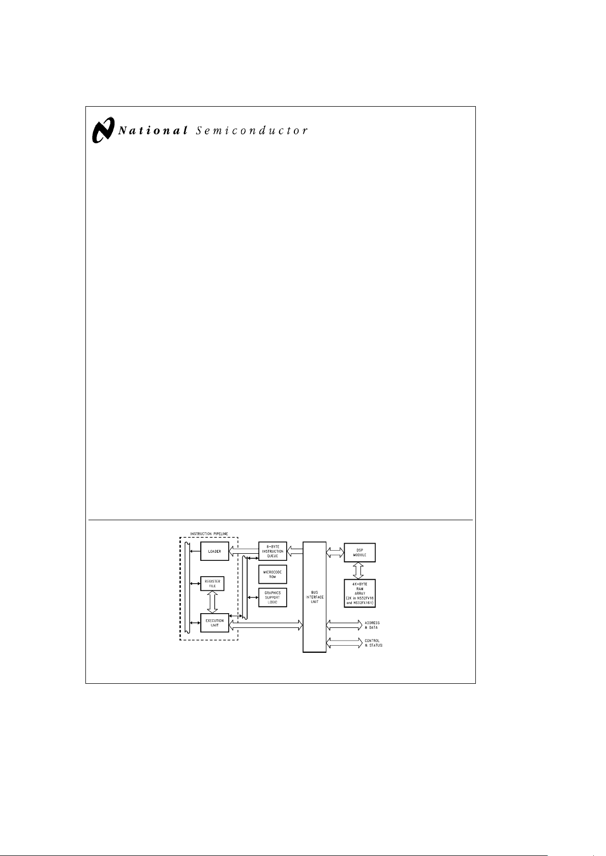
The NS32FX164, the NS32FV16 and the NS32FX161 are
high-performance 32-bit members of the Series 32000
É
/
EP
TM
family of National’s Embedded System Processors
TM
specifically optimized for CCITT Group 2 and Group 3 Facsimile Applications, Data Modems, Voice Mail Systems, Laser Printers, or any combination of the above.
Unless specified otherwise any reference to the
NS32FX164 in this document applies to the NS32FV16 and
the NS32FX161 as well.
The NS32FX164 can perform all the computations and control functions required for a stand-alone Fax system, a PC
add-in Fax/Voice/Data Modem card or a Laser/Fax system.
It also meets the performance requirements to implement
14400, 9600 and 7200 bps modems complying with CCITT
V.17, V.29 and V.27 standards. The NS32FV16 supports
V.29 and V.27 standards as well as voice. The NS32FX161
supports V.29 and V.27 standards.
The NS32FX164 provides a 16 Mbyte Linear external address space and a 16-bit external data bus.
The CPU core, which is the same as that of the NS32CG16,
incorporates a 32-bit ALU and instruction pipeline, and an
8-byte prefetch queue.
Also integrated on-chip with the CPU are a DSP Module
(DSPM) and a 4K-byte RAM Array (2K in the NS32FV16 and
NS32FX161). The DSPM is a complete processing unit, capable of autonomous operation parallel to the CPU core
operation. The DSPM executes programs stored in an internal on-chip Random Access Memory (RAM), and manipulates data stored either in the internal RAM or in an external
off-chip memory. To maximize utilization of hardware resources, the DSPM contains a pipelined DSP-oriented datapath, and a control logic that implements a set of DSP vector commands.
The NS32FX164 capabilities can be expanded by using an
external floating point unit (FPU) which directly interfaces to
the NS32FX164 using the slave protocol. The CPU-FPU
cluster features high speed execution of the floating-point
instructions.
The NS32FX164 highly-efficient architecture combined with
the NS32CG16 graphics instructions and the high-performance vector operation capability, makes the device the ideal
choice for Postscript
TM
and Fax applications.
Features
Y
Software compatible with the Series 32000/EP
processors
Y
Designed around the CPU core of the NS32CG16
Y
Pin compatible with the NS32FX16
Y
32-bit architecture and implementation
Y
On-chip DSP Module for high-speed DSP operations
Y
Special support for graphics applications
Ð 18 graphics instructions
Ð Binary compression/expansion capability for font
storage using RLL encoding
Ð Pattern magnification
Ð Interface to an external BITBLT processing units for
fast color BITBLT operations
Y
4K-byte on-chip RAM array (2K in NS32FV16 and
NS32FX161)
Y
On-chip clock generator
Y
Floating-point support via the NS32081 or NS32181
Y
Optimal interface to large memory arrays via the
NS32CG821 and the DP84xx family of DRAM
controllers
Y
Power save mode
Y
High-speed CMOS technology
Y
68-pin PLCC package
Block Diagram
TL/EE/11267– 1
FIGURE 1-1. CPU Block Diagram
Series 32000Éis a registered trademark of National Semiconductor Corporation.
EP
TM
and Embedded System ProcessorsTMare trademarks of National Semiconductor Corporation.
Postscript
TM
is a trademark of Adobe Systems, Inc.
C
1995 National Semiconductor Corporation RRD-B30M115/Printed in U. S. A.
Page 2

Table of Contents
1.0 PRODUCT INTRODUCTION АААААААААААААААААААААА6
1.1 NS32FX164 Special Features АААААААААААААААААААА6
2.0 ARCHITECTURAL DESCRIPTION ААААААААААААААААА7
2.1 Register Set ААААААААААААААААААААААААААААААААААА7
2.1.1 General Purpose Registers ААААААААААААААААА7
2.1.2 Address Registers ААААААААААААААААААААААААА8
2.1.3 Processor Status Register АААААААААААААААААА8
2.1.4 Configuration Register ААААААААААААААААААААА9
2.1.5 DSP Module Registers ААААААААААААААААААААА9
2.2 Memory Organization АААААААААААААААААААААААААА11
2.2.1 Address MappingААААААААААААААААААААААААА12
2.3 Modular Software Support АААААААААААААААААААААА12
2.4 Instruction Set АААААААААААААААААААААААААААААААА12
2.4.1 General Instruction Format АААААААААААААААА12
2.4.2 Addressing ModesАААААААААААААААААААААААА14
2.4.3 Instruction Set Summary АААААААААААААААААА16
2.5 Graphics SupportАААААААААААААААААААААААААААААА20
2.5.1 Frame Buffer Addressing АААААААААААААААААА20
2.5.2 BITBLT Fundamentals АААААААААААААААААААА20
2.5.2.1 Frame Buffer ArchitectureААААААААААА21
2.5.2.2 Bit Alignment АААААААААААААААААААААА21
2.5.2.3 Block Boundaries and Destination
MasksАААААААААААААААААААААААААААА21
2.5.2.4 BITBLT Directions ААААААААААААААААА22
2.5.2.5 BITBLT Variations ААААААААААААААААА23
2.5.3 Graphics Support Instructions АААААААААААААА23
2.5.3.1 BITBLT (BIT-aligned BLock Transfer)À23
2.5.3.2 Pattern Fill АААААААААААААААААААААААА24
2.5.3.3 Data Compression, Expansion and
MagnifyААААААААААААААААААААААААААА24
2.5.3.3.1 Magnifying Compressed
Data ААААААААААААААААААААА26
3.0 FUNCTIONAL DESCRIPTION АААААААААААААААААААА26
3.1 Instruction Execution АААААААААААААААААААААААААА26
3.1.1 Operating States ААААААААААААААААААААААААА26
3.1.2 Instruction Endings ААААААААААААААААААААААА26
3.1.2.1 Completed Instructions ААААААААААААА27
3.1.2.2 Suspended InstructionsААААААААААААА27
3.1.2.3 Terminated InstructionsААААААААААААА27
3.1.2.4 Partially Completed Instructions ААААА27
3.1.3 Slave Processor Instructions ААААААААААААААА27
3.1.3.1 Slave Processor Protocol ААААААААААА27
3.1.3.2 Floating-Point Instructions АААААААААА28
3.2 Exception Processing АААААААААААААААААААААААААА29
3.2.1 Exception Acknowledge Sequence ААААААААА29
3.2.2 Returning from an Exception Service
Procedure ААААААААААААААААААААААААААААААА30
3.2.3 Maskable InterruptsААААААААААААААААААААААА34
3.2.3.1 Non-Vectored Mode ААААААААААААААА34
3.2.3.2 Vectored Mode: Non-Cascaded
Case ААААААААААААААААААААААААААААА35
3.2.3.3 Vectored Mode: Cascaded Case ААААА35
3.2.4 Non-Maskable Interrupt ААААААААААААААААААА37
3.2.5 Traps ААААААААААААААААААААААААААААААААААА37
3.2.6 Priority among Exceptions ААААААААААААААААА37
3.2.7 Exception Acknowledge Sequences: Detailed
Flow АААААААААААААААААААААААААААААААААААА39
3.2.7.1 Maskable/Non-Maskable Interrupt
Sequence АААААААААААААААААААААААА39
3.2.7.2 SLAVE/ILL/SVC/DVZ/FLG/BPT/UND
Trap Sequence АААААААААААААААААААА39
3.2.7.3 Trace Trap Sequence АААААААААААААА39
3.3 Debugging Support АААААААААААААААААААААААААААА40
3.3.1 Instruction TracingАААААААААААААААААААААААА40
3.4 DSP Module АААААААААААААААААААААААААААААААААА40
3.4.1 Programming Model АААААААААААААААААААААА40
3.4.2 RAM Organization and Data Types ААААААААА41
3.4.2.1 Integer ValuesААААААААААААААААААААА41
3.4.2.2 Aligned-Integer Values ААААААААААААА41
3.4.2.3 Real Values ААААААААААААААААААААААА41
3.4.3.4 Aligned-Real Values ААААААААААААААА41
3.4.2.5 Extended Precision Real Values ААААА41
3.4.2.6 Complex Values ААААААААААААААААААА42
3.4.3 Command List Format АААААААААААААААААААА42
3.4.4 CPU Core Interface ААААААААААААААААААААААА42
3.4.4.1 Synchronization of Parallel OperationÀ42
3.4.4.2 DSPM RAM Organization ААААААААААА43
3.4.5 DSPM Instruction Set ААААААААААААААААААААА43
3.4.5.1 Conventions АААААААААААААААААААААА43
3.4.5.2 Type Casting АААААААААААААААААААААА43
3.4.5.3 General NotesААААААААААААААААААААА44
3.4.5.4 Load Register Instructions АААААААААА44
3.4.5.5 Store Register Instructions АААААААААА45
3.4.5.6 Adjust Register Instructions ААААААААА46
3.4.5.7 Flow Control Instructions ААААААААААА47
3.4.5.8 Internal Memory Move Instructions ÀÀÀ48
3.4.5.9 External Memory Move Instructions ÀÀ48
3.4.5.10 Arithmetic/Logical Instructions ААААА49
3.4.5.11 Multiply-and-Accumulate
Instructions АААААААААААААААААААААА49
3.4.5.12 Multiply-and-Add InstructionsААААААА50
3.4.5.13 Clipping and Min/Max Instructions ÀÀ52
3.4.5.14 Special Instructions ААААААААААААААА53
2
Page 3

Table of Contents (Continued)
3.5 System Interface АААААААААААААААААААААААААААААА55
3.5.1 Power and Grounding ААААААААААААААААААААА55
3.5.2 Clocking АААААААААААААААААААААААААААААААА56
3.5.3 Power Save Mode АААААААААААААААААААААААА57
3.5.4 ResettingАААААААААААААААААААААААААААААААА57
3.5.5 Bus Cycles АААААААААААААААААААААААААААААА58
3.5.5.1 Bus Status АААААААААААААААААААААААА58
3.5.5.2 Basic Read and Write Cycles АААААААА58
3.5.5.3 Cycle Extension ААААААААААААААААААА62
3.5.5.4 Instruction Fetch Cycles АААААААААААА63
3.5.5.5 Interrupt Control CyclesААААААААААААА64
3.5.5.6 Special Bus CyclesААААААААААААААААА65
3.5.5.7 Slave Processor Bus CyclesААААААААА65
3.5.5.8 Data Access Sequences АААААААААААА67
3.5.5.9 Bus Access Control АААААААААААААААА68
3.5.5.10 Instruction Status ААААААААААААААААА71
4.0 DEVICE SPECIFICATIONS АААААААААААААААААААААА71
4.1 NS32FX164 Pin Descriptions ААААААААААААААААААА71
4.1.1 Supplies АААААААААААААААААААААААААААААААА71
4.1.2 Input SignalsААААААААААААААААААААААААААААА71
4.1.3 Output Signals ААААААААААААААААААААААААААА71
4.1.4 Input-Output Signals АААААААААААААААААААААА72
4.2 Absolute Maximum Ratings ААААААААААААААААААААА74
4.3 Electrical Characteristics ААААААААААААААААААААААА74
4.4 Switching Characteristics ААААААААААААААААААААААА74
4.4.1 Definitions ААААААААААААААААААААААААААААААА74
4.4.2 Timing TablesАААААААААААААААААААААААААААА75
4.4.2.1 Output Signals: Internal Propagation
Delays ААААААААААААААААААААААААААА75
4.4.2.2 Input Signal Requirements АААААААААА77
4.4.3 Timing Diagrams ААААААААААААААААААААААААА79
APPENDIX A: INSTRUCTION FORMATS ААААААААААААА89
APPENDIX B: INSTRUCTION EXECUTION TIMESААААА92
B.1 Basic and Floating-Point Instructions АААААААААААА92
B.1.1 Equations ААААААААААААААААААААААААААААААА92
B.1.2 Notes on Table Use АААААААААААААААААААААА93
B.1.3 Calculation of the Execution Time TEX for Basic
Instructions ААААААААААААААААААААААААААААА93
B.1.4 Calculation of the Execution Time TEX for
Floating-Point InstructionsААААААААААААААААА93
B.2 Special Graphics Instructions ААААААААААААААААААА99
B.2.1 Execution Time Calculation for Special
Graphics Instructions ААААААААААААААААААААА99
B.3 DSPM Instructions ААААААААААААААААААААААААААА100
List of Figures
FIGURE 1-1. CPU Block Diagram АААААААААААААААААААААААААААААААААААААААААААААААААААААААААААААААААААААААААААААААА1
FIGURE 2-1. NS32FX164 Internal Registers ААААААААААААААААААААААААААААААААААААААААААААААААААААААААААААААААААААААА7
FIGURE 2-2. Processor Status Register (PSR) ААААААААААААААААААААААААААААААААААААААААААААААААААААААААААААААААААААА8
FIGURE 2-3. Configuration Register (CFG) АААААААААААААААААААААААААААААААААААААААААААААААААААААААААААААААААААААААА9
FIGURE 2-4. DSP Module Registers Address MapАААААААААААААААААААААААААААААААААААААААААААААААААААААААААААААААААА9
FIGURE 2-5. Accumulator Format АААААААААААААААААААААААААААААААААААААААААААААААААААААААААААААААААААААААААААААААА9
FIGURE 2-6. X, Y, Z Registers Format АААААААААААААААААААААААААААААААААААААААААААААААААААААААААААААААААААААААААААА9
FIGURE 2-7. EABR Register FormatААААААААААААААААААААААААААААААААААААААААААААААААААААААААААААААААААААААААААААА10
FIGURE 2-8. OVF Register Format АААААААААААААААААААААААААААААААААААААААААААААААААААААААААААААААААААААААААААААА10
FIGURE 2-9. PARAM Register Format ААААААААААААААААААААААААААААААААААААААААААААААААААААААААААААААААААААААААААА10
FIGURE 2-10. REPEAT Register Format АААААААААААААААААААААААААААААААААААААААААААААААААААААААААААААААААААААААААА10
FIGURE 2-11. EXT Register Format АААААААААААААААААААААААААААААААААААААААААААААААААААААААААААААААААААААААААААААА11
FIGURE 2-12. CLSTAT Register Format АААААААААААААААААААААААААААААААААААААААААААААААААААААААААААААААААААААААААА11
FIGURE 2-13. DSPINT and DSPMASK Register Format ААААААААААААААААААААААААААААААААААААААААААААААААААААААААААААА11
FIGURE 2-14. NMISTAT Register Format ААААААААААААААААААААААААААААААААААААААААААААААААААААААААААААААААААААААААА11
FIGURE 2-15. NS32FX164 Address Mapping АААААААААААААААААААААААААААААААААААААААААААААААААААААААААААААААААААААА12
FIGURE 2-16. NS32FX164 Run-Time Environment ААААААААААААААААААААААААААААААААААААААААААААААААААААААААААААААААА13
FIGURE 2-17. General Instruction Format ААААААААААААААААААААААААААААААААААААААААААААААААААААААААААААААААААААААААА13
FIGURE 2-18. Index Byte FormatААААААААААААААААААААААААААААААААААААААААААААААААААААААААААААААААААААААААААААААААА13
FIGURE 2-19. Displacement Encodings ААААААААААААААААААААААААААААААААААААААААААААААААААААААААААААААААААААААААААА14
FIGURE 2-20. Correspondence between Linear and Cartesian Addressing АААААААААААААААААААААААААААААААААААААААААААА20
FIGURE 2-21. 32-Pixel by 32-Scan Line Frame Buffer ААААААААААААААААААААААААААААААААААААААААААААААААААААААААААААААА21
FIGURE 2-22. Overlapping BITBLT Blocks АААААААААААААААААААААААААААААААААААААААААААААААААААААААААААААААААААААААА22
FIGURE 2-23. BB Instructions Format АААААААААААААААААААААААААААААААААААААААААААААААААААААААААААААААААААААААААААА23
FIGURE 2-24. BITWT Instruction Format АААААААААААААААААААААААААААААААААААААААААААААААААААААААААААААААААААААААААА24
FIGURE 2-25. EXTBLT Instruction Format ААААААААААААААААААААААААААААААААААААААААААААААААААААААААААААААААААААААААА24
FIGURE 2-26. MOVMPi Instruction Format АААААААААААААААААААААААААААААААААААААААААААААААААААААААААААААААААААААААА24
3
Page 4

List of Figures (Continued)
FIGURE 2-27. TBITS Instruction FormatААААААААААААААААААААААААААААААААААААААААААААААААААААААААААААААААААААААААААА24
FIGURE 2-28. SBITS Instruction Format АААААААААААААААААААААААААААААААААААААААААААААААААААААААААААААААААААААААААА25
FIGURE 2-29. SBITPS Instruction Format ААААААААААААААААААААААААААААААААААААААААААААААААААААААААААААААААААААААААА25
FIGURE 2-30. Bus Activity for a Simple BITBLT Operation ААААААААААААААААААААААААААААААААААААААААААААААААААААААААААА25
FIGURE 3-1. Operating States АААААААААААААААААААААААААААААААААААААААААААААААААААААААААААААААААААААААААААААААААА26
FIGURE 3-2. Slave Processor Protocol АААААААААААААААААААААААААААААААААААААААААААААААААААААААААААААААААААААААААА28
FIGURE 3-3. Slave Processor Status Word ААААААААААААААААААААААААААААААААААААААААААААААААААААААААААААААААААААААА29
FIGURE 3-4. Interrupt Dispatch and Cascade Tables АААААААААААААААААААААААААААААААААААААААААААААААААААААААААААААА30
FIGURE 3-5. Exception Acknowledge Sequence: Direct-Exception Mode Disabled АААААААААААААААААААААААААААААААААААА31
FIGURE 3-6. Exception Acknowledge Sequence: Direct-Exception Mode Enabled ААААААААААААААААААААААААААААААААААААА32
FIGURE 3-7. Return from Trap (RETTn) Instruction Flow: Direct-Exception Mode Disabled ААААААААААААААААААААААААААААА33
FIGURE 3-8. Return from Interrupt (RETI) Instruction Flow: Direct-Exception Mode Disabled АААААААААААААААААААААААААААА34
FIGURE 3-9. Interrupt Control Unit Connections (16 Levels) АААААААААААААААААААААААААААААААААААААААААААААААААААААААА35
FIGURE 3-10. Cascaded Interrupt Control Unit Connections ААААААААААААААААААААААААААААААААААААААААААААААААААААААААА36
FIGURE 3-11. Exception Processing Flowchart АААААААААААААААААААААААААААААААААААААААААААААААААААААААААААААААААААА38
FIGURE 3-12. Service Sequence ААААААААААААААААААААААААААААААААААААААААААААААААААААААААААААААААААААААААААААААААА39
FIGURE 3-13. DSP Module Block Diagram АААААААААААААААААААААААААААААААААААААААААААААААААААААААААААААААААААААААА55
FIGURE 3-14. Power and Ground ConnectionsААААААААААААААААААААААААААААААААААААААААААААААААААААААААААААААААААААА56
FIGURE 3-15. Crystal InterconnectionsР30 MHz АААААААААААААААААААААААААААААААААААААААААААААААААААААААААААААААААА56
FIGURE 3-16. Crystal InterconnectionsР40 MHz, 50 MHz ААААААААААААААААААААААААААААААААААААААААААААААААААААААААААА56
FIGURE 3-17. Recommended Reset Connections АААААААААААААААААААААААААААААААААААААААААААААААААААААААААААААААААА56
FIGURE 3-18. Power-On Reset Requirements ААААААААААААААААААААААААААААААААААААААААААААААААААААААААААААААААААААА57
FIGURE 3-19. General Reset TimingАААААААААААААААААААААААААААААААААААААААААААААААААААААААААААААААААААААААААААААА57
FIGURE 3-20. Bus Connections АААААААААААААААААААААААААААААААААААААААААААААААААААААААААААААААААААААААААААААААААА59
FIGURE 3-21. Read Cycle Timing АААААААААААААААААААААААААААААААААААААААААААААААААААААААААААААААААААААААААААААААА60
FIGURE 3-22. Write Cycle Timing АААААААААААААААААААААААААААААААААААААААААААААААААААААААААААААААААААААААААААААААА61
FIGURE 3-23. Cycle Extension of a Read Cycle АААААААААААААААААААААААААААААААААААААААААААААААААААААААААААААААААААА63
FIGURE 3-24. Special Bus Cycle Timing АААААААААААААААААААААААААААААААААААААААААААААААААААААААААААААААААААААААААА65
FIGURE 3-25. Slave Processor Read Cycle АААААААААААААААААААААААААААААААААААААААААААААААААААААААААААААААААААААААА66
FIGURE 3-26. Slave Processor Write Cycle АААААААААААААААААААААААААААААААААААААААААААААААААААААААААААААААААААААААА67
FIGURE 3-27. NS32FX164 and FPU Interconnections АААААААААААААААААААААААААААААААААААААААААААААААААААААААААААААА67
FIGURE 3-28. Memory Interface ААААААААААААААААААААААААААААААААААААААААААААААААААААААААААААААААААААААААААААААААА67
FIGURE 3-29. HOLD
Timing (Bus Initially Idle) ААААААААААААААААААААААААААААААААААААААААААААААААААААААААААААААААААААА69
FIGURE 3-30. HOLD Timing (Bus Initially Not Idle) АААААААААААААААААААААААААААААААААААААААААААААААААААААААААААААААААА70
FIGURE 4-1. Connection DiagramААААААААААААААААААААААААААААААААААААААААААААААААААААААААААААААААААААААААААААААА73
FIGURE 4-2. Output Signals Specification Standard ААААААААААААААААААААААААААААААААААААААААААААААААААААААААААААААА74
FIGURE 4-3a. Input Signals Specification Standard ААААААААААААААААААААААААААААААААААААААААААААААААААААААААААААААААА74
FIGURE 4-3b. RSTI
, INT, NMI HysteresisАААААААААААААААААААААААААААААААААААААААААААААААААААААААААААААААААААААААААА74
FIGURE 4-4. Read CycleААААААААААААААААААААААААААААААААААААААААААААААААААААААААААААААААААААААААААААААААААААААА79
FIGURE 4-5. Write Cycle ААААААААААААААААААААААААААААААААААААААААААААААААААААААААААААААААААААААААААААААААААААААА80
FIGURE 4-6. Special Bus Cycle ААААААААААААААААААААААААААААААААААААААААААААААААААААААААААААААААААААААААААААААААА81
FIGURE 4-7. HOLD
Acknowledge Timing (Bus Initially Not Idle) ААААААААААААААААААААААААААААААААААААААААААААААААААААА82
FIGURE 4-8. HOLD Timing (Bus Initially Idle) ААААААААААААААААААААААААААААААААААААААААААААААААААААААААААААААААААААА83
FIGURE 4-9. External DMA Controller Bus Cycle АААААААААААААААААААААААААААААААААААААААААААААААААААААААААААААААААА84
FIGURE 4-10. Slave Processor Write Timing ААААААААААААААААААААААААААААААААААААААААААААААААААААААААААААААААААААААА85
FIGURE 4-11. Slave Processor Read Timing ААААААААААААААААААААААААААААААААААААААААААААААААААААААААААААААААААААААА85
FIGURE 4-12. SPC
Timing АААААААААААААААААААААААААААААААААААААААААААААААААААААААААААААААААААААААААААААААААААААА85
FIGURE 4-13. PFS Signal Timing ААААААААААААААААААААААААААААААААААААААААААААААААААААААААААААААААААААААААААААААААА86
FIGURE 4-14. ILO Signal Timing ААААААААААААААААААААААААААААААААААААААААААААААААААААААААААААААААААААААААААААААААА86
FIGURE 4-15. Clock Waveforms ААААААААААААААААААААААААААААААААААААААААААААААААААААААААААААААААААААААААААААААААА86
FIGURE 4-16. INT
Signal Timing ААААААААААААААААААААААААААААААААААААААААААААААААААААААААААААААААААААААААААААААААА87
4
Page 5

List of Figures (Continued)
FIGURE 4-17. NMI
Signal TimingААААААААААААААААААААААААААААААААААААААААААААААААААААААААААААААААААААААААААААААААА87
FIGURE 4-18. Power-On Reset АААААААААААААААААААААААААААААААААААААААААААААААААААААААААААААААААААААААААААААААААА87
FIGURE 4-19. Non-Power-On Reset АААААААААААААААААААААААААААААААААААААААААААААААААААААААААААААААААААААААААААААА88
FIGURE 4-20. Interrupt Out АААААААААААААААААААААААААААААААААААААААААААААААААААААААААААААААААААААААААААААААААААААА88
List of Tables
TABLE 2-1. NS32FX164 Addressing Modes ААААААААААААААААААААААААААААААААААААААААААААААААААААААААААААААААААААААА15
TABLE 2-2. NS32FX164 Instruction Set Summary АААААААААААААААААААААААААААААААААААААААААААААААААААААААААААААААААА16
TABLE 2-3. ‘op’ and ‘i’ Field Encodings ААААААААААААААААААААААААААААААААААААААААААААААААААААААААААААААААААААААААААА23
TABLE 3-1. Floating-Point Instruction Protocols АААААААААААААААААААААААААААААААААААААААААААААААААААААААААААААААААААА28
TABLE 3-2. Summary of Exception ProcessingААААААААААААААААААААААААААААААААААААААААААААААААААААААААААААААААААААА40
TABLE 3-3. External Oscillator Specifications Crystal Characteristics ААААААААААААААААААААААААААААААААААААААААААААААААА57
TABLE 3-4. Interrupt Sequences ААААААААААААААААААААААААААААААААААААААААААААААААААААААААААААААААААААААААААААААААА64
TABLE 3-5. Bus Cycle Categories АААААААААААААААААААААААААААААААААААААААААААААААААААААААААААААААААААААААААААААААА67
TABLE 3-6. Data Access Sequences ААААААААААААААААААААААААААААААААААААААААААААААААААААААААААААААААААААААААААААА68
TABLE B-1. Basic Instructions ААААААААААААААААААААААААААААААААААААААААААААААААААААААААААААААААААААААААААААААААААА94
TABLE B-2. Floating-Point Instructions: CPU Portion АААААААААААААААААААААААААААААААААААААААААААААААААААААААААААААААА98
TABLE B-3. Average Instruction Execution Times with No Wait-States АААААААААААААААААААААААААААААААААААААААААААААААА99
TABLE B-4. Average Instruction Execution Times with Wait-States АААААААААААААААААААААААААААААААААААААААААААААААААА100
5
Page 6

1.0 Product Introduction
The NS32FX164 is a high speed CMOS microprocessor in
the Series 32000/EP family.
It includes two main execution units: the NS32CG16 compatible CPU core and the DSP Module. The CPU core is
designed for general purpose computations and system
control functions. The DSP Module is tuned to perform the
DSP primitives needed in Voice Band Modems. The
NS32FX164 also incorporates a 4K-byte RAM Array as a
shared resource for both the CPU core and the DSP Module
(2K-byte in the NS32FV16 and the NS32FX161).
The NS32FX164 is software-compatible with all other CPUs
in the family.
The device incorporates all of the Series 32000 advanced
architectural features, with the exception of the virtual memory capability.
Brief descriptions of the NS32FX164 features that are
shared with other members of the family are provided below:
Powerful Addressing Modes. Nine addressing modes
available to all instructions are included to access data
structures efficiently.
Data Types. The architecture provides for numerous data
types, such as byte, word, doubleword, and BCD, which may
be arranged into a wide variety of data structures.
Symmetric Instruction Set. While avoiding special case
instructions that compilers can’t use, the Series 32000 family incorporates powerful instructions for control operations,
such as array indexing and external procedure calls, which
save considerable space and time for compiled code.
Memory-to-Memory Operations. The Series 32000 CPUs
represent two-address machines. This means that each operand can be referenced by any one of the addressing
modes provided.
This powerful memory-to-memory architecture permits
memory locations to be treated as registers for all useful
operations. This is important for temporary operands as well
as for context switching.
Large, Uniform Addressing. The NS32FX164 has 24-bit
address pointers that can address up to 16 megabytes without any segmentation; this addressing scheme provides
flexible memory management without add-on expense.
Modular Software Support. Any software package for the
Series 32000 architecture can be developed independent of
all other packages, without regard to individual addressing.
In addition, ROM code is totally relocatable and easy to
access, which allows a significant reduction in hardware and
software cost.
Software Processor Concept. The Series 32000 architecture allows future expansions of the instruction set that can
be executed by special slave processors, acting as exten-
sions to the CPU. This concept of slave processors is
unique to the Series 32000 architecture. It allows software
compatibility even for future components because the slave
hardware is transparent to the software. With future advances in semiconductor technology, the slaves can be
physically integrated on the CPU chip itself.
To summarize, the architectural features cited above provide three primary performance advantages and characteristics:
#
High-Level Language Support
#
Easy Future Growth Path
#
Application Flexibility
1.1 NS32FX164 SPECIAL FEATURES
In addition to the above Series 32000 features, the
NS32FX164 provides features that make the device extremely attractive for a wide range of applications where
graphics support, low chip count, and low power consumption are required.
The most relevant of these features are the enhanced Digital Signal Processing performance which makes the chip
very attractive for facsimile applications, and the graphics
support capabilities, that can be used in applications such
as printers, CRT terminals, and other varieties of display
systems, where text and graphics are to be handled.
Graphics support is provided by eighteen instructions that
allow operations such as BITBLT, data compression/expansion, fills, and line drawing, to be performed very efficiently.
In addition, the device can be easily interfaced to an external BITBLT Processing Unit (BPU) for high BITBLT performance.
The NS32FX164 allows systems to be built with a relatively
small amount of random logic. The bus is highly optimized
to allow simple interfacing to a large variety of DRAMs and
peripheral devices. All the relevant bus access signals and
clock signals are generated on-chip. The cycle extension
logic is also incorporated on-chip.
The device is fabricated in a low-power, high speed CMOS
technology. It also includes a power-save feature that allows the clock to be slowed down under software control,
thus minimizing the power consumption. This feature can be
used in those applications where power saving during periods of low performance demand is highly desirable.
The power save feature, the DSP Module and the Bus Characteristics are described in the ‘‘Functional Description’’
section. A general overview of BITBLT operations and a
description of the graphics support instructions is provided
in Section 2.5. Details on all the NS32FX164 graphics instructions can be found in the NS32CG16 Printer/Display
Processor Programmer’s Reference Supplement.
6
Page 7

1.0 Product Introduction (Continued)
Below is a summary of the instructions that are directly applicable to graphics along with their intended use.
Instruction Application
BBAND The BITBLT group of instructions provide a
BBOR method of quickly imaging characters,
BBFOR creating patterns, windowing and other
BBXOR block oriented effects.
BBSTOD
BITWT
EXTBLT
MOVMP Move Multiple Pattern is a very fast
instruction for clearing memory and drawing
patterns and lines.
TBITS Test Bit String will measure the length of 1’s
or 0’s in an image, supporting many data
compression methods (RLL), TBITS may
also be used to test for boundaries of
images.
SBITS Set Bit String is a very fast instruction for
filling objects, outline characters and
drawing horizontal lines.
The TBITS and SBITS instructions support
Group 3 and Group 4 CCITT standards for
compression and decompression
algorithms.
SBITPS Set Bit Perpendicular String is a very fast
instruction for drawing vertical, horizontal
and 45
§
lines.
In printing applications SBITS and SBITPS
may be used to express portrait and
landscape respectively from the same
compressed font data. The size of the
character may be scaled as it is drawn.
SBIT The Bit group of instructions enable single
CBIT pixels anywhere in memory to be set,
TBIT cleared, tested or inverted.
IBIT
INDEX The INDEX instruction combines a multiply-
add sequence into a single instruction. This
provides a fast translation of an X-Y
address to a pixel relative address.
2.0 Architectural Description
2.1 REGISTER SET
The NS32FX164 has 32 internal registers. 17 of these registers belong to the CPU portion of the device and are addressed either implicitly by specific instructions or through
the register addressing mode. The other 15 control the operation of the DSP Module, and are memory mapped.
Figure
2-1
shows the NS32FX164 internal registers.
CPU Registers
General Purpose
w
32 Bits
x
R0–R7
Address
PC
SP0, SP1
FP
SB
INTBASE
MOD
Processor Status
PSR
Configuration
CFG
Peripherals Registers
DSP Module
A
X
Y
Z
EABR
CLPTR
OVF
PARAM
REPEAT
ABORT
EXT
CLSTAT
DSPINT
DSPMASK
NMISTAT
FIGURE 2-1. NS32FX164 Internal Registers
2.1.1 General Purpose Registers
There are eight registers (R0 – R7) used for satisfying the
high speed general storage requirements, such as holding
temporary variables and addresses. The general purpose
registers are free for any use by the programmer. They are
32 bits in length. If a general purpose register is specified for
an operand that is 8 or 16 bits long, only the low part of the
register is used; the high part is not referenced or modified.
7
Page 8

2.0 Architectural Description (Continued)
2.1.2 Address Registers
The seven address registers are used by the processor to
implement specific address functions. Except for the MOD
register that is 16 bits wide, all the others are 32 bits. A
description of the address registers follows.
PCÐProgram Counter. The PC register is a pointer to the
first byte of the instruction currently being executed. The PC
is used to reference memory in the program section.
SP0, SP1ÐStack Pointers. The SP0 register points to the
lowest address of the last item stored on the INTERRUPT
STACK. This stack is normally used only by the operating
system. It is used primarily for storing temporary data, and
holding return information for operating system subroutines
and interrupt and trap service routines. The SP1 register
points to the lowest address of the last item stored on the
USER STACK. This stack is used by normal user programs
to hold temporary data and subroutine return information.
When a reference is made to the selected Stack Pointer
(see PSR S-bit), the terms ‘‘SP Register’’ or ‘‘SP’’ are used.
SP refers to either SP0 or SP1, depending on the setting of
the S bit in the PSR register. If the S bit in the PSR is 0, SP
refers to SP0. If the S bit in the PSR is 1 then SP refers to
SP1.
Stacks in the Series 32000 architecture grow downward in
memory. A Push operation pre-decrements the Stack Pointer by the operand length. A Pop operation post-increments
the Stack Pointer by the operand length.
FPÐFrame Pointer. The FP register is used by a procedure
to access parameters and local variables on the stack. The
FP register is set up on procedure entry with the ENTER
instruction and restored on procedure termination with the
EXIT instruction.
The frame pointer holds the address in memory occupied by
the old contents of the frame pointer.
SBÐStatic Base. The SB register points to the global variables of a software module. This register is used to support
relocatable global variables for software modules. The SB
register holds the lowest address in memory occupied by
the global variables of a module.
INTBASEÐInterrupt Base. The INTBASE register holds
the address of the dispatch table for interrupts and traps
(Section 3.2.1).
MODÐModule. The MOD register holds the address of the
module descriptor of the currently executing software module. The MOD register is 16 bits long, therefore the module
table must be contained within the first 64 kbytes of memory.
2.1.3 Processor Status Register
The Processor Status Register (PSR) holds status information for the microprocessor.
The PSR is sixteen bits long, divided into two eight-bit
halves. The low order eight bits are accessible to all programs, but the high order eight bits are accessible only to
programs executing in Supervisor Mode.
15 8 7 0
BIPSUNZFJKLTC
FIGURE 2-2. Processor Status Register (PSR)
C The C bit indicates that a carry or borrow occurred after
an addition or subtraction instruction. It can be used with
the ADDC and SUBC instructions to perform multipleprecision integer arithmetic calculations. It may have a
setting of 0 (no carry or borrow) or 1 (carry or borrow).
T The T bit causes program tracing. If this bit is set to 1, a
TRC trap is executed after every instruction (Section
3.3.1).
L The L bit is altered by comparison instructions. In a com-
parison instruction the L bit is set to ‘‘1’’ if the second
operand is less than the first operand, when both operands are interpreted as unsigned integers. Otherwise, it
is set to ‘‘0’’. In Floating-Point comparisons, this bit is
always cleared.
K Reserved for use by the CPU.
J Reserved for use by the CPU.
F The F bit is a general condition flag, which is altered by
many instructions (e.g., integer arithmetic instructions
use it to indicate overflow).
Z The Z bit is altered by comparison instructions. In a com-
parison instruction the Z bit is set to ‘‘1’’ if the second
operand is equal to the first operand; otherwise it is set
to ‘‘0’’.
N The N bit is altered by comparison instructions. In a
comparison instruction the N bit is set to ‘‘1’’ if the second operand is less than the first operand, when both
operands are interpreted as signed integers. Otherwise,
it is set to ‘‘0’’.
U If the U bit is ‘‘1’’ no privileged instructions may be exe-
cuted. If the U bit is ‘‘0’’ then all instructions may be
executed. When U
e
0 the processor is said to be in Su-
pervisor Mode; when U
e
1 the processor is said to be in
User Mode. A User Mode program is restricted from executing certain instructions and accessing certain registers which could interfere with the operating system. For
example, a User Mode program is prevented from
changing the setting of the flag used to indicate its own
privilege mode. A Supervisor Mode program is assumed
to be a trusted part of the operating system, hence it has
no such restrictions.
S The S bit specifies whether the SP0 register or SP1 reg-
ister is used as the Stack Pointer. The bit is automatically cleared on interrupts and traps. It may have a setting
of 0 (use the SP0 register) or 1 (use the SP1 register).
P The P bit prevents a TRC trap from occurring more than
once for an instruction (Section 3.3.1). It may have a
setting of 0 (no trace pending) or 1 (trace pending).
I If I
e
1, then all interrupts will be accepted. If Ie0, only
the NMI interrupt is accepted. Trap enables are not affected by this bit.
8
Page 9
2.0 Architectural Description (Continued)
B Reserved for use by the CPU. This bit is set to 1 during
the execution of the EXTBLT instruction and causes the
BPU
signal to become active. Upon reset, B is set to
zero and the BPU
signal is set high.
Note 1: When an interrupt is acknowledged, the B, I, P, S and U bits are set
to zero and the BPU
signal is set high. A return from interrupt will
restore the original values from the copy of the PSR register saved
in the interrupt stack.
Note 2: If BITBLT (BB) or EXTBLT instructions are executed in an interrupt
routine, the PSR bits J and K must be cleared first.
2.1.4 Configuration Register
The Configuration Register (CFG) is 32 bits wide, of which 5
bits are implemented. The implemented bits enable various
operating modes for the CPU, including vectoring of interrupts, execution of floating-point instructions, processing of
exceptions and selection of clock scaling factor. The CFG is
programmed by the SETCFG instruction. The format of CFG
is shown in
Figure 2-3
. The various control bits are de-
scribed below.
31 8 7 0
Reserved DE Res C M F I
FIGURE 2-3. Configuration Register (CFG)
I Interrupt vectoring. This bit controls whether maskable
interrupts are handled in nonvectored (I
e
0) or vec-
tored (I
e
1) mode. Refer to Section 3.2.3 for more in-
formation.
F Floating-point instruction set. This bit indicates wheth-
er a floating-point unit (FPU) is present to execute
floating-point instructions. If this bit is 0 when the CPU
executes a floating-point instruction, a Trap (UND) occurs. If this bit is 1, then the CPU transfers the instruction and any necessary operands to the FPU using the
slave-processor protocol described in Section 3.1.3.1.
M Clock scaling. This bit is used in conjunction with the
C-bit to select the clock scaling factor.
C Clock scaling. Same as the M-bit above. Refer to Sec-
tion 3.5.3 on ‘‘Power Save Mode’’ for details.
DE Direct-Exception mode enable. This bit enables the Di-
rect-Exception mode for processing exceptions. When
this mode is selected, the CPU response time to interrupts and other exceptions is significantly improved.
Refer to Section 3.2 for more information.
2.1.5 DSP Module Registers
The DSP Module (DSPM) contains 15 memory-mapped registers. All the registers, except OVF, CLSTAT, ABORT,
DSPINT and NMISTAT, are readable and writable. OVF,
CLSTAT, DSPINT and NMISTAT are read-only. ABORT is
write-only.
The DSPM registers are divided into two groups, according
to their function. PARAM, OVF, X, Y, Z, A, REPEAT, CLPTR
and EABR are called DSPM dedicated registers. CLSTAT,
ABORT, DSPINT, DSPMASK, EXT and NMISTAT are called
CPU core interface registers.
Accesses to these registers must be aligned; word and double-word accesses must occur on word and double-word
address boundaries respectively. Failing to do so will cause
unpredictable results.
Figure 2-4
shows the address map of
the DSP Module registers.
Register Register
Name Address
PARAM FFFF8000
OVF FFFF8004
X FFFF8008
Y FFFF800C
Z FFFF8010
A FFFF8014
REPEAT FFFF8018
CLPTR FFFF8020
EABR FFFF8024
CLSTAT FFFF9000
ABORT FFFF9004
DSPINT FFFF9008
DSPMASK FFFF900C
EXT FFFF9010
NMISTAT FFFF9014
FIGURE 2-4. DSP Module Registers Address Map
AÐAccumulator
The format of the accumulator is shown in
Figure 2-5
.
33 0 33 0
Imaginary Real
FIGURE 2-5. Accumulator Format
The A register is a complex accumulator. It has two 34-bit
fields: a real part, and an imaginary part. Bits 15 through 30
of the real and the imaginary parts of the accumulator can
be read or written by the core in one double-word access.
Bits 15 through 30 of the real part are mapped to the operand’s bits 0 through 15, and bits 15 through 30 of the imaginary part are mapped to the operand’s bits 16 through 31.
The accumulator can also be read and written by the command-list execution unit using the SA, SEA, LA and LEA
instructions (See Section 3.4 for more information).
Note that when a value is stored in the accumulator by the
core, the value of PARAM.RND bit is copied into bit position
14 of both real and imaginary parts of the accumulator. This
technique allows rounding of the accumulator’s value in the
following DSPM instructions (See Section 3.4.5.3 for more
information on rounding).
When the Accumulator is loaded either by the core or by the
LA or LEA instructions, bits 31– 33 of the real and the imaginary accumulators are loaded with the values of bit 30 of the
real and the imaginary parts respectively.
When the Accumulator is loaded either by the core or by the
LA instruction, bits 0 – 13 of the real and the imaginary accumulators are loaded with zeros.
X, Y, ZÐVector Pointers
The format of X, Y, and Z registers is shown in
Figure 2-6
.
31 16 15 8 7 4 3 0
ADDRESS Reserved WRAP-AROUND INCREMENT
FIGURE 2-6. X, Y, Z Registers Format
9
Page 10
2.0 Architectural Description (Continued)
The X, Y, and Z registers are used for addressing up to
three vector operands. They are 32-bit registers, with three
fields: ADDRESS, INCREMENT, and WRAP-AROUND. The
value in the ADDRESS field specifies the address of a word
in the on-chip memory. This field has 16 bits, and can address up to 64 Kwords of internal memory. The ADDRESS
fields are initialized with the vector operands’ start-addresses by commands in the command list. At the beginning of
each vector operation, the contents of the ADDRESS field
are copied to incrementors. Increments can be used by vector instructions to step through the corresponding vector
operands while executing the appropriate calculations.
There is an address wrap-around for those vector instructions that require some of their operands to be located in
cyclic buffers. The allowed values for the increment field are
0 through 15. The actual increment will be 2
increment
words.
The allowed values for the WRAP-AROUND field are 0
through 15. The actual wrap-around will be 2
WRAP-AROUND
words. The WRAP-AROUND must be greater or equal to
the INCREMENT.
The X, Y, and Z registers can be read and written by the
core. These registers can be read and written by the command-list execution unit, as well as by the core, when using
SX, SXL, SXH, SY, SZ, LX, LY and LZ instructions.
EABRÐExternal Address Base Register
The format of the external address base register is shown in
Figure 2-7
.
31 17 16 0
ADDRESS 0
FIGURE 2-7. EABR Register Format
The EABR register is used together with a 16-bit address
field to form a 32-bit external address. External addresses
are specified as the sum of the value in EABR and two times
the value of the 16-bit address pointed by registers X, Y or
Z. The only value allowed to be written into bits 0 through 16
of EABR is ‘‘0’’. The EABR register can be read and written
by the core. It can also be written by the command-list execution unit by using the LEABR instruction.
EABR can hold any value except for FFFE0000. Accessing
external memory with an FFFE0000 in the EABR will cause
unpredictable results.
CLPTRÐCommand List Pointer
The CLPTR is a 16-bit register that holds the address of the
current command in the internal RAM. Writing into the
CLPTR causes the DSPM command-list execution unit to
begin executing commands, starting from the address in
CLPTR. The CLPTR can be read and written by the core
while the command-list execution is idle.
Whenever the DSPM command-list execution unit reads a
command from the DSPM RAM, the value of CLPTR is updated to contain the address of the next command to be
executed. This implies, for example, that if the last command in a list is in address N, the CLPTR will hold a value of
N
a
1 following the end of command list execution.
OVFÐOverflow Register
The format of the overflow register is shown in
Figure 2-8
.
15 2 1 0
Reserved OVF SAT
FIGURE 2-8. OVF Register Format
The OVF register holds the current status of the DSPM
arithmetic unit. It has two fields: OVF and SAT. The OVF bit
is set to ‘‘1’’ whenever an overflow is detected in the DSPM
34-bit ALU (e.g., bits 32 and 33 of the ALU are not equal).
No overflow detection is provided for integers. The SAT bit
is set to ‘‘1’’ whenever a value read from the accumulator
cannot be represented within the limits of its data type (e.g.,
16 bits for real and integer, and 31 bits for extended real). In
this case the value read from the accumulator will either be
the maximum allowed value or the minimal allowed value for
this data type depending on the sign of the accumulator
value. Note that in some cases when the OVF is set, the
SAT will not be set. The reason is that if an OVF occurred,
the value in the accumulator can no longer be used for
proper SAT detection. Upon reset, and whenever the
ABORT register is written, the non reserved bits of the OVF
register is cleared to ‘‘0’’.
The OVF is a read only register. It can be read by the core. It
can also be read by the command-list execution unit using
the SOVF instruction. Reading the OVF by either the core or
the command-list execution unit clears it to ‘‘0’’.
PARAMÐVector Parameter Register
The format of the PARAM register is shown in Figure 2-9.
31 26 25 24 19 18 17 16 15 0
Reserved RND OP SUB CLR COJ LENGTH
FIGURE 2-9. PARAM Register Format
The PARAM register is used to specify the number of iterations and special options for the various instructions. The
options are: RND, OP, SUB, CLR, and COJ. The effect of
each of the bits of the PARAM register is specified in Section 3.4.
The PARAM register can be read and written by the core. It
can also be written by the command-list execution unit, by
using the LPARAM instruction. The value written into PARAM.LENGTH must be greater then 0.
The value of PARAM.LENGTH is not changed during command-list execution, unless it is written into using the
LPARAM instruction.
REPEATÐCommand-List Repeat Register
The format of the repeat register is shown in
Figure 2-10
.
31 16 15 0
COUNT TARGET
FIGURE 2-10. REPEAT Register Format
The REPEAT register is used, together with appropriate
commands, to implement loops and branches in the command list. The count is used to specify the number of times
a loop in the command list is to be repeated. The target is
used to specify a jump address within the command list.
The REPEAT register can be read and written by the core. It
can also be read and written by the command-list execution
unit by using SREPEAT and LREPEAT instructions respectively.
The value of REPEAT.COUNT changes during the execution of the DJNZ command.
ABORTÐAbort Register
The ABORT register is used to force execution of the command list to halt. Writing any value into this register stops
execution, and clears the contents of OVF, EXT, DSPINT
and DSPMASK. The ABORT register can only be written
and only by the core.
10
Page 11
2.0 Architectural Description (Continued)
EXTÐExternal Memory Reference Control Register
The format of the external memory reference control register is shown in
Figure 2-11
.
15 1 0
Reserved HOLD
FIGURE 2-11. EXT Register Format
The EXT register controls external references. The command-list execution unit checks the value of EXT.HOLD before each external memory reference. When EXT.HOLD is
‘‘0’’, external memory references are allowed. When
EXT.HOLD is ‘‘1’’, and external memory references are requested, the execution of the command list will stop until
EXT.HOLD is ‘‘0’’. Upon reset, and whenever the ABORT
register is written, EXT.HOLD is cleared to ‘‘0’’. The EXT
register can be read or written by the core.
CLSTATÐCommand-List Execution Status Register
The format of the command-list execution status register is
shown in
Figure 2-12
.
15 1 0
Reserved RUN
FIGURE 2-12. CLSTAT Register Format
The CLSTAT register displays the current status of the execution of the command list. When the command-list execution is idle, CLSTAT.RUN is ‘‘0’’, and when it is active,
CLSTAT.RUN is ‘‘1’’. Upon reset, the CLSTAT register is
cleared to ‘‘0’’. It can only be read, and only by the core.
DSPINT, DSPMASK, NMISTATÐInterrupt Control
Registers
The format of DSPINT and DSPMASK is shown in
Figure
2-13
.
15 1 0
Reserved HALT
FIGURE 2-13. DSPINT and DSPMASK Register Format
The DSPINT register holds the current status of interrupt
requests. Whenever execution of the command list is
stopped, the DSPINT.HALT bit is set to ‘‘1’’. The DSPINT is
a read only register. It is cleared to ‘‘0’’ whenever it is read,
whenever the ABORT register is written, and upon reset.
The DSPMASK register is used to mask the DSPINT. HALT
flag. An interrupt request is transferred to the interrupt logic
of the IOUT
output pin whenever the DSPINT.HALT bit is
set to ‘‘1’’, and the DSPMASK.HALT bit is unmasked (set to
‘‘1’’). See Section 4.0 for the functionality of IOUT
.
DSPMASK can be read and written by the core. Upon reset,
and whenever the ABORT register is written, all the bits in
DSPMASK are cleared to ‘‘0’’.
The format of the NMISTAT register is shown in
Figure 2-14
.
15 3 2 1 0
Reserved ERR UND EXT
FIGURE 2-14. NMISTAT Register Format
The NMISTAT holds the status of the current pending NonMaskable Interrupt (NMI) requests.
Whenever the core attempts to access the DSPM address
space while the CLSTAT.RUN bit is ‘‘1’’ (except for accesses to the CLSTAT, EXT, DSPINT, NMISTAT, DSPMASK,
and ABORT registers) NMISTAT.ERR is set to ‘‘1’’.
Whenever there is an attempt to execute a DBPT instruction, or a reserved DSPM instruction (Section 3.4), the
NMISTAT.UND bit is set to ‘‘1’’.
When a high to low transition is detected on the NMI
input
pin, NMISTAT.EXT bit is set to ‘‘1’’.
When one of the bits in NMISTAT is set to ‘‘1’’, an NMI
request to the core is issued.
The NMISTAT register is cleared to 0 upon reset, and each
time its contents are read.
When one of the bits in NMISTAT is set to 1, an NMI occurs.
The NMI handler can read the NMISTAT register to determine the source of the interrupt. Note that since NMIs may
be nested, it is possible that a second NMI handler (invoked
while the previous handler has not yet exited) will read and
handle more than one set bit in NMISTAT. Since the read
operation clears the register, the interrupted handler may
find that no bits are set.
2.2 MEMORY ORGANIZATION
The main memory of the NS32FX164 is a uniform linear
address space. Memory locations are numbered sequentially starting at zero and ending at 2
24
b
1. The number specifying a memory location is called an address. The contents
of each memory location is a byte consisting of eight bits.
Unless otherwise noted, diagrams in this document show
data stored in memory with the lowest address on the right
and the highest address on the left. Also, when data is
shown vertically, the lowest address is at the top of a diagram and the highest address at the bottom of the diagram.
When bits are numbered in a diagram, the least significant
bit is given the number zero, and is shown at the right of the
diagram. Bits are numbered in increasing significance and
toward the left.
70
A
Byte at Address A
Two contiguous bytes are called a word. Except where noted, the least significant byte of a word is stored at the lower
address, and the most significant byte of the word is stored
at the next higher address. In memory, the address of a
word is the address of its least significant byte, and a word
may start at any address.
15 8 7 0
Aa1A
MSB LSB
Word at Address A
Two contiguous words are called a double-word. Except
where noted, the least significant word of a double-word is
stored at the lowest address and the most significant word
of the double-word is stored at the address two higher. In
memory, the address of a double-word is the address of its
least significant byte, and a double-word may start at any
address.
31 24 23 16 15 8 7 0
Aa3A
a
2A
a
1A
MSB LSB
Double Word at Address A
11
Page 12

2.0 Architectural Description (Continued)
Although memory is addressed as bytes, it is actually organized as words. Therefore, words and double-words that are
aligned to start at even addresses (multiples of two) are
accessed more quickly than words and double-words that
are not so aligned.
2.2.1 Address Mapping
The NS32FX164 supports the use of memory-mapped peripheral devices and coprocessors. Such memory-mapped
devices can be located at arbitrary locations within the
16-Mbyte address range available externally.
Addresses marked as Reserved in
Figure 2-15
are not available in the present implementation of the NS32FX164, and
should not be used. The top 8-Mbyte block is reserved by
National Semiconductor Corporation, and only a few locations within this block are presently used to access the onchip RAM array and DSP Module registers.
Figure 2-15
shows the NS32FX164 address mapping.
Start Address
(HEX)
00000000 Memory and I/O
00FFFE00 Interrupt Control
01000000 Reserved
FFFE0000 DSPM Internal RAM
FFFE1000 Reserved
FFFF8000 DSPM Dedicated Registers
FFFF8028 Reserved
FFFF9000 DSPM Control/Status Registers
FFFF9014 Reserved
FIGURE 2-15. NS32FX164 Address Mapping
2.3 MODULAR SOFTWARE SUPPORT
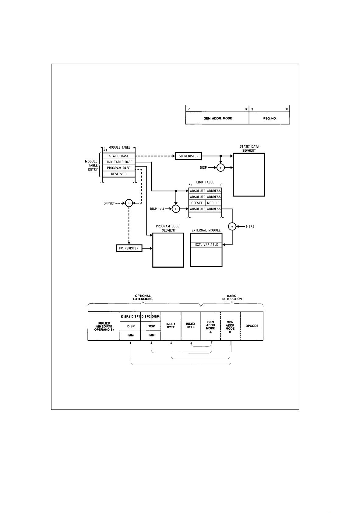
The NS32FX164 provides special support for software modules and modular programs.
Each module in a NS32FX164 software environment consists of three components:
1. Program Code Segment.
This segment contains the module’s code and constant
data.
2. Static Data Segment.
Used to store variables and data that may be accessed
by all procedures within the module.
3. Link Table.
This component contains two types of entries: Absolute
Addresses and Procedure Descriptors.
An Absolute Address is used in the external addressing
mode, in conjunction with a displacement and the current
MOD Register contents to compute the effective address
of an external variable belonging to another module.
The Procedure Descriptor is used in the call external procedure (CXP) instruction to compute the address of an
external procedure.
Normally, the linker program specifies the locations of the
three components. The Static Data and Link Table typically
reside in RAM; the code component can be either in RAM or
in ROM. The three components can be mapped into noncontiguous locations in memory, and each can be independently relocated. Since the Link Table contains the absolute
addresses of external variables, the linker need not assign
absolute memory addresses for these in the module itself;
they may be assigned at load time.
To handle the transfer of control from one module to another, the NS32FX164 uses a module table in memory and two
registers in the CPU.
The Module Table is located within the first 64 kbytes of
memory. This table contains a Module Descriptor (also
called a Module Table Entry) for each module in the address space of the program. A Module Descriptor has four
32-bit entries corresponding to each component of a module:
#
The Static Base entry contains the address of the beginning of the module’s static data segment.
#
The Link Table Base points to the beginning of the module’s Link Table.
#
The Program Base is the address of the beginning of the
code and constant data for the module.
#
A fourth entry is currently unused but reserved.
The MOD Register in the CPU contains the address of the
Module Descriptor for the currently executing module.
The Static Base Register (SB) contains a copy of the Static
Base entry in the Module Descriptor of the currently executing module, i.e., it points to the beginning of the current
module’s static data area.
This register is implemented in the CPU for efficiency purposes. By having a copy of the static base entry or chip, the
CPU can avoid reading it from memory each time a data
item in the static data segment is accessed.
In an NS32FX164 software environment modules need not
be linked together prior to loading. As modules are loaded,
a linking loader simply updates the Module Table and fills
the Link Table entries with the appropriate values. No modification of a module’s code is required. Thus, modules may
be stored in read-only memory and may be added to a system independently of each other, without regard to their individual addressing.
Figure 2-16
shows a typical
NS32FX164 run-time environment.
2.4 INSTRUCTION SET
2.4.1 General Instruction Format
Figure 2-17
shows the general format of a Series 32000
instruction. The Basic Instruction is one to three bytes long
and contains the Opcode and up to two 5-bit General Addressing Mode (‘‘Gen’’) fields. Following the Basic Instruction field is a set of optional extensions, which may appear
depending on the instruction and the addressing modes selected.
Index Bytes appear when either or both Gen fields specify
Scaled Index. In this case, the Gen field specifies only the
Scale Factor (1, 2, 4 or 8), and the Index Byte specifies
which General Purpose Register to use as the index, and
which addressing mode calculation to perform before indexing.
12
Page 13
2.0 Architectural Description (Continued)
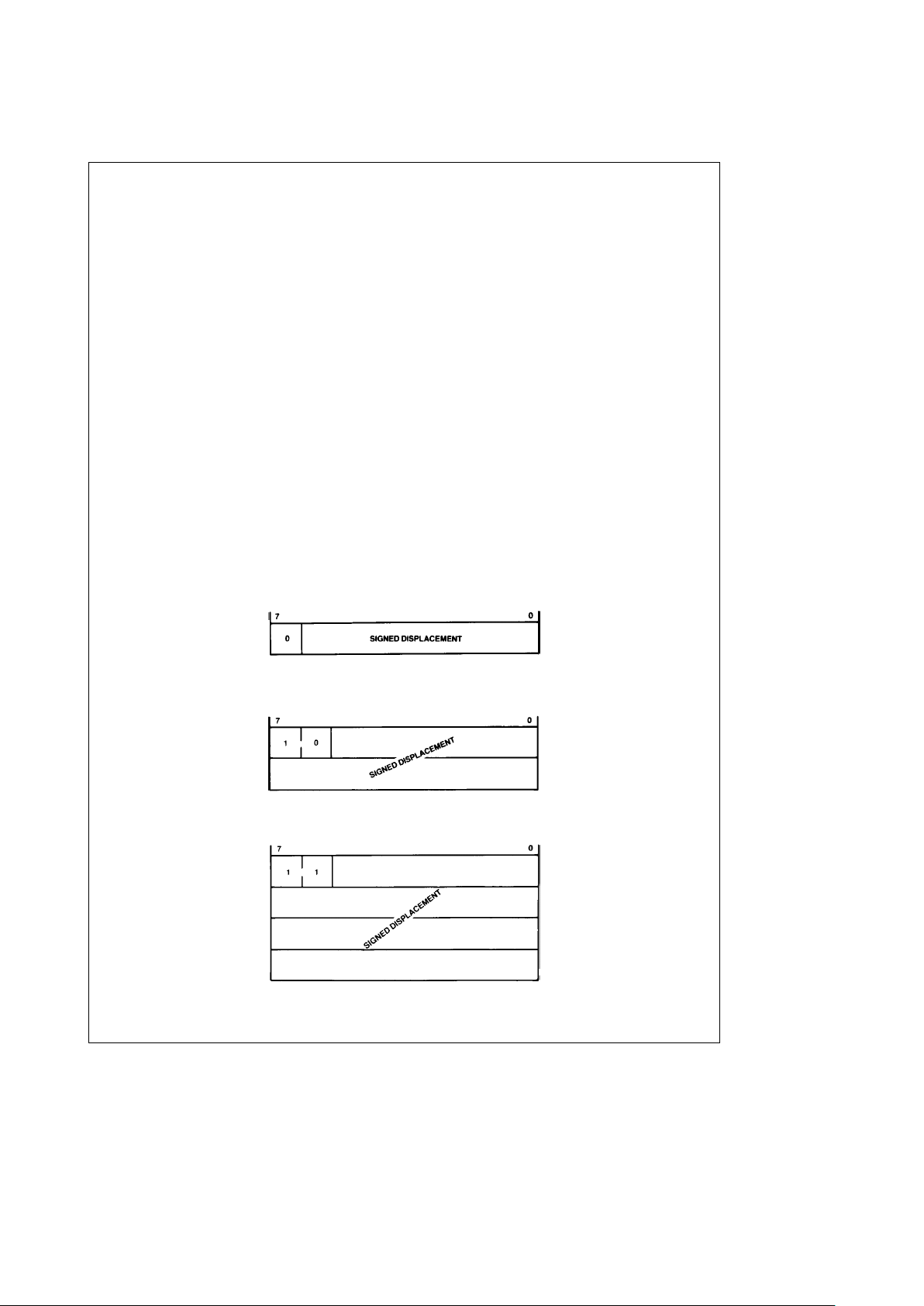
Following Index Bytes come any displacements (addressing
constants) or immediate values associated with the selected addressing modes. Each Disp/lmm field may contain
one of two displacements, or one immediate value. The size
of a Displacement field is encoded within the top bits of that
field, as shown in
Figure 2-19
, with the remaining bits interpreted as a signed (two’s complement) value. The size of an
immediate value is determined from the Opcode field. Both
Displacement and Immediate fields are stored most-significant byte first. Note that this is different from the memory
representation of data (Section 2.2).
Some instructions require additional ‘‘implied’’ immediates
and/or displacements, apart from those associated with addressing modes. Any such extensions appear at the end of
the instruction, in the order that they appear within the list of
operands in the instruction definition (Section 2.4.3).
TL/EE/11267– 3
FIGURE 2-18. Index Byte Format
TL/EE/11267– 2
Note: Dashed lines indicate information copied to register during transfer of control between modules.
FIGURE 2-16. NS32FX164 Run-Time Environment
TL/EE/11267– 4
FIGURE 2-17. General Instruction Format
13
Page 14
2.0 Architectural Description (Continued)
2.4.2 Addressing Modes
The NS32FX164 CPU generally accesses an operand by
calculating its Effective Address based on information available when the operand is to be accessed. The method to be
used in performing this calculation is specified by the programmer as an ‘‘addressing mode’’.
Addressing modes in the NS32FX164 are designed to optimally support high-level language accesses to variables. In
nearly all cases, a variable access requires only one addressing mode, within the instruction that acts upon that
variable. Extraneous data movement is therefore minimized.
NS32FX164 Addressing Modes fall into nine basic types:
Register: The operand is available in one of the eight General Purpose Registers. In certain Slave Processor instructions, an auxiliary set of eight registers may be referenced
instead.
Register Relative: A General Purpose Register contains an
address to which is added a displacement value from the
instruction, yielding the Effective Address of the operand in
memory.
Memory Space: Identical to Register Relative above, except that the register used is one of the dedicated registers
PC, SP, SB or FP. These registers point to data areas generally needed by high-level languages.
Memory Relative: A pointer variable is found within the
memory space pointed to by the SP, SB or FP register. A
displacement is added to that pointer to generate the Effective Address of the operand.
Immediate: The operand is encoded within the instruction.
This addressing mode is not allowed if the operand is to be
written.
Absolute: The address of the operand is specified by a
displacement field in the instruction.
External: A pointer value is read from a specified entry of
the current Link Table. To this pointer value is added a displacement, yielding the Effective Address of the operand.
Top of Stack: The currently-selected Stack Pointer (SP0 or
SP1) specifies the location of the operand. The operand is
pushed or popped, depending on whether it is written or
read.
Scaled Index: Although encoded as an addressing mode,
Scaled Indexing is an option on any addressing mode except Immediate or another Scaled Index. It has the effect of
calculating an Effective Address, then multiplying any General Purpose Register by 1, 2, 4 or 8 and adding into the
total, yielding the final Effective Address of the operand.
Table 2-1 is a brief summary of the addressing modes. For a
complete description of their actions, see the Series 32000
Instruction Set Reference Manual.
In addition to the general modes, Register-Indirect with
auto-increment/decrement and warps or pitch are available
on several of the graphics instructions.
Byte Displacement: Range
b
64 toa63
Word Displacement: Range
b
8192 toa8191
Double Word Displacement:
Range (Entire Addressing Space)
TL/EE/11267– 5
FIGURE 2-19. Displacement Encodings
14
Page 15

2.0 Architectural Description (Continued)
TABLE 2-1. NS32FX164 Addressing Modes
ENCODING MODE ASSEMBLER SYNTAX EFFECTIVE ADDRESS
Register
00000 Register 0 R0 or F0 None: Operand is in the specified
00001 Register 1 R1 or F1 register.
00010 Register 2 R2 or F2
00011 Register 3 R3 or F3
00100 Register 4 R4 or F4
00101 Register 5 R5 or F5
00110 Register 6 R6 or F6
00111 Register 7 R6 or F7
Register Relative
01000 Register 0 relative disp(R0) Disp
a
Register.
01001 Register 1 relative disp(R1)
01010 Register 2 relative disp(R2)
01011 Register 3 relative disp(R3)
01100 Register 4 relative disp(R4)
01101 Register 5 relative disp(R5)
01110 Register 6 relative disp(R6)
01111 Register 7 relative disp(R7)
Memory Relative
10000 Frame memory relative disp2(disp1 (FP)) Disp2
a
Pointer; Pointer found at
10001 Stack memory relative disp2(disp1 (SP)) address Disp 1
a
Register. ‘‘SP’’
10010 Static memory relative disp2(disp1 (SB)) is either SP0 or SP1, as selected
in PSR.
Reserved
10011 (Reserved for Future Use)
Immediate
10100 Immediate value None: Operand is input from
instruction queue.
Absolute
10101 Absolute
@
disp Disp.
External
10110 External EXT (disp1)
a
disp2 Disp2aPointer; Pointer is found
at Link Table Entry number Disp1.
Top Of Stack
10111 Top of stack TOS Top of current stack, using either
User or Interrupt Stack Pointer,
as selected in PSR. Automatic
Push/Pop included.
Memory Space
11000 Frame memory disp(FP) Disp
a
Register; ‘‘SP’’ is either
11001 Stack memory disp(SP) SP0 or SP1, as selected in PSR.
11010 Static memory disp(SB)
11011 Program memory *
a
disp
Scaled Index
11100 Index, bytes mode[Rn:B
]
EA (mode)
a
Rn.
11101 Index, words mode[Rn:W
]
EA (mode)
a
2cRn.
11110 Index, double words mode[Rn:D
]
EA (mode)
a
4cRn.
11111 Index, quad words mode[Rn:Q
]
EA (mode)
a
8cRn.
‘‘Mode’’ and ‘‘n’’ are contained
within the Index Byte.
EA (mode) denotes the effective
address generated using mode.
15
Page 16

2.0 Architectural Description (Continued)
2.4.3 Instruction Set Summary
Table 2-2 presents a brief description of the NS32FX164
instruction set. The Format column refers to the Instruction
Format tables (Appendix A). The Instruction column gives
the instruction as coded in assembly language, and the Description column provides a short description of the function
provided by that instruction. Further details of the exact operations performed by each instruction may be found in the
Series 32000 Instruction Set Reference Manual and the
NS32CG16 Printer/Display Processor Programmer’s Reference.
Notations:
i
e
Integer length suffix: BeByte
W
e
Word
D
e
Double Word
f
e
Floating Point length suffix: FeStandard Floating
L
e
Long Floating
gen
e
General operand. Any addressing mode can be speci-
fied.
short
e
A 4-bit value encoded within the Basic Instruction
(see Appendix A for encodings).
imm
e
Implied immediate operand. An 8-bit value appended
after any addressing extensions.
disp
e
Displacement (addressing constant): 8, 16 or 32 bits.
All three lengths legal.
reg
e
Any General Purpose Register: R0– R7.
areg
e
Any Processor Register: SP, SB, FP, INTBASE,
MOD, PSR, US (bottom 8 PSR bits).
cond
e
Any condition code, encoded as a 4-bit field within
the Basic Instruction (see Appendix A for encodings).
TABLE 2-2. NS32FX164 Instruction Set Summary
MOVES
Format Operation Operands Description
4 MOVi gen,gen Move a value.
2 MOVQi short,gen Extend and move a signed 4-bit constant.
7 MOVMi gen,gen,disp Move multiple: disp bytes (1 to 16).
7 MOVZBW gen,gen Move with zero extension.
7 MOVZiD gen,gen Move with zero extension.
7 MOVXBW gen,gen Move with sign extension.
7 MOVXiD gen,gen Move with sign extension.
4 ADDR gen,gen Move effective address.
INTEGER ARITHMETIC
Format Operation Operands Description
4 ADDi gen,gen Add.
2 ADDQi short,gen Add signed 4-bit constant.
4 ADDCi gen,gen Add with carry.
4 SUBi gen,gen Subtract.
4 SUBCi gen,gen Subtract with carry (borrow).
6 NEGi gen,gen Negate (2’s complement).
6 ABSi gen,gen Take absolute value.
7 MULi gen,gen Multiply.
7 QUOi gen,gen Divide, rounding toward zero.
7 REMi gen,gen Remainder from QUO.
7 DIVi gen,gen Divide, rounding down.
7 MODi gen,gen Remainder from DIV (Modulus).
7 MEIi gen,gen Multiply to extended integer.
7 DEIi gen,gen Divide extended integer.
PACKED DECIMAL (BCD) ARITHMETIC
Format Operation Operands Description
6 ADDPi gen,gen Add packed.
6 SUBPi gen,gen Subtract packed.
16
Page 17

2.0 Architectural Description (Continued)
TABLE 2-2. NS32FX164 Instruction Set Summary (Continued)
INTEGER COMPARISON
Format Operation Operands Description
4 CMPi gen,gen Compare.
2 CMPQi short,gen Compare to signed 4-bit constant.
7 CMPMi gen,gen,disp Compare multiple: disp bytes (1 to 16).
LOGICAL AND BOOLEAN
Format Operation Operands Description
4 ANDi gen,gen Logical AND.
4 ORi gen,gen Logical OR.
4 BICi gen,gen Clear selected bits.
4 XORi gen,gen Logical exclusive OR.
6 COMi gen,gen Complement all bits.
6 NOTi gen,gen Boolean complement: LSB only.
2 Scondi gen Save condition code (cond) as a Boolean variable of size i.
SHIFTS
Format Operation Operands Description
6 LSHi gen,gen Logical shift, left or right.
6 ASHi gen,gen Arithmetic shift, left or right.
6 ROTi gen,gen Rotate, left or right.
BIT FIELDS
Bit fields are values in memory that are not aligned to byte boundaries. Examples are PACKED arrays and records used in
Pascal. ‘‘Extract’’ instructions read and align a bit field. ‘‘Insert’’ instructions write a bit field from an aligned source.
Format Operation Operands Description
8 EXTi reg,gen,gen,disp Extract bit field (array oriented).
8 INSi reg,gen,gen,disp Insert bit field (array oriented).
7 EXTSi gen,gen,imm,imm Extract bit field (short form).
7 INSSi gen,gen,imm,imm Insert bit field (short form).
8 CVTP reg,gen,gen Convert to bit field pointer.
ARRAYS
Format Operation Operands Description
8 CHECKi reg,gen,gen Index bounds check.
8 INDEXi reg,gen,gen Recursive indexing step for multiple-dimensional arrays.
STRINGS
String instructions assign specific functions to the General
Purpose Registers:
R4 Ð Comparison Value
R3 Ð Translation Table Pointer
R2 Ð String 2 Pointer
R1 Ð String 1 Pointer
R0 Ð Limit Count
Options on all string instructions are:
B (Backward): Decrement string pointers after each
step rather than incrementing.
U (Until match): End instruction if String 1 entry matches
R4.
W (While match): End instruction if String 1 entry does not
match R4.
All string instructions end when R0 decrements to zero.
17
Page 18

2.0 Architectural Description (Continued)
TABLE 2-2. NS32FX164 Instruction Set Summary (Continued)
Format Operation Operands Description
5 MOVSi options Move string 1 to string 2.
MOVST options Move string, translating bytes.
5 CMPSi options Compare string 1 to string 2.
CMPST options Compare, translating string 1 bytes.
5 SKPSi options Skip over string 1 entries.
SKPST options Skip, translating bytes for until/while.
JUMPS AND LINKAGE
Format Operation Operands Description
3 JUMP gen Jump.
0 BR disp Branch (PC Relative).
0 Bcond disp Conditional branch.
3 CASEi gen Multiway branch.
2 ACBi short,gen,disp Add 4-bit constant and branch if non-zero.
3 JSR gen Jump to subroutine.
1 BSR disp Branch to subroutine.
1 CXP disp Call external procedure
3 CXPD gen Call external procedure using descriptor.
1 SVC Supervisor call.
1 FLAG Flag trap.
1 BPT Breakpoint trap.
1 ENTER
[
reg list], disp Save registers and allocate stack frame (Enter Procedure).
1 EXIT
[
reg list
]
Restore registers and reclaim stack frame (Exit Procedure).
1 RET disp Return from subroutine.
1 RXP disp Return from external procedure call.
1 RETT disp Return from trap. (Privileged)
1 RETI Return from interrupt. (Privileged)
CPU REGISTER MANIPULATION
Format Operation Operands Description
1 SAVE
[
reg list
]
Save general purpose registers.
1 RESTORE
[
reg list
]
Restore general purpose registers.
2 LPRi areg,gen Load dedicated register. (Privileged if PSR or INTBASE)
2 SPRi areg,gen Store dedicated register. (Privileged if PSR or INTBASE)
3 ADJSPi gen Adjust stack pointer.
3 BISPSRi gen Set selected bits in PSR. (Privileged if not Byte length)
3 BICPSRi gen Clear selected bits in PSR. (Privileged if not Byte length)
5 SETCFG
[
option list
]
Set configuration register. (Privileged)
18
Page 19

2.0 Architectural Description (Continued)
TABLE 2-2. NS32FX164 Instruction Set Summary (Continued)
FLOATING POINT
Format Operation Operands Description
11 MOVf gen,gen Move a floating point value.
9 MOVLF gen,gen Move and shorten a long value to standard.
9 MOVFL gen,gen Move and lengthen a standard value to long.
9 MOVif gen,gen Convert any integer to standard or long floating.
9 ROUNDfi gen,gen Convert to integer by rounding.
9 TRUNCfi gen,gen Convert to integer by truncating, toward zero.
9 FLOORfi gen,gen Convert to largest integer less than or equal to value.
11 ADDf gen,gen Add.
11 SUBf gen,gen Subtract.
11 MULf gen,gen Multiply.
11 DIVf gen,gen Divide.
11 CMPf gen,gen Compare.
11 NEGf gen,gen Negate.
11 ABSf gen,gen Take absolute value.
9 LFSR gen Load FSR.
9 SFSR gen Store FSR.
12 POLYf gen,gen Polynomial Step.
12 DOTf gen,gen Dot Product.
12 SCALBf gen,gen Binary Scale.
12 LOGBf gen,gen Binary Log.
MISCELLANEOUS
Format Operation Operands Description
1 NOP No operation.
1 WAIT Wait for interrupt.
1 DIA Diagnose. Single-byte ‘‘Branch to Self’’ for hardware
breakpointing. Not for use in programming.
GRAPHICS
Format Operation Operands Description
5 BBOR options* Bit-aligned block transfer ‘OR’.
5 BBAND options Bit-aligned block transfer ‘AND’.
5 BBFOR Bit-aligned block transfer fast ‘OR’.
5 BBXOR options Bit-aligned block transfer ‘XOR’.
5 BBSTOD options Bit-aligned block source to destination.
5 BITWT Bit-aligned word transfer.
5 EXTBLT options External bit-aligned block transfer.
5 MOVMPi Move multiple pattern.
5 TBITS options Test bit string.
5 SBITS Set bit string.
5 SBITPS Set bit perpendicular string.
BITS
Format Operation Operands Description
4 TBITi gen,gen Test bit.
6 SBITi gen,gen Test and set bit.
6 SBITIi gen,gen Test and set bit, interlocked.
6 CBITi gen,gen Test and clear bit.
6 CBITIi gen,gen Test and clear bit, interlocked.
6 IBITi gen,gen Test and invert bit.
8 FFSi gen,gen Find first set bit.
*Note: Options are controlled by fields of the instruction, PSR status bits, or dedicated register values.
19
Page 20
2.0 Architectural Description (Continued)
2.5 GRAPHICS SUPPORT
The following sections provide a brief description of the
NS32FX164 graphics support capabilities. Basic discussions on frame buffer addressing and BITBLT operations
are also provided. More detailed information on the
NS32FX164 graphics support instructions can be found in
the NS32CG16 Printer/Display Processor Programmer’s
Reference.
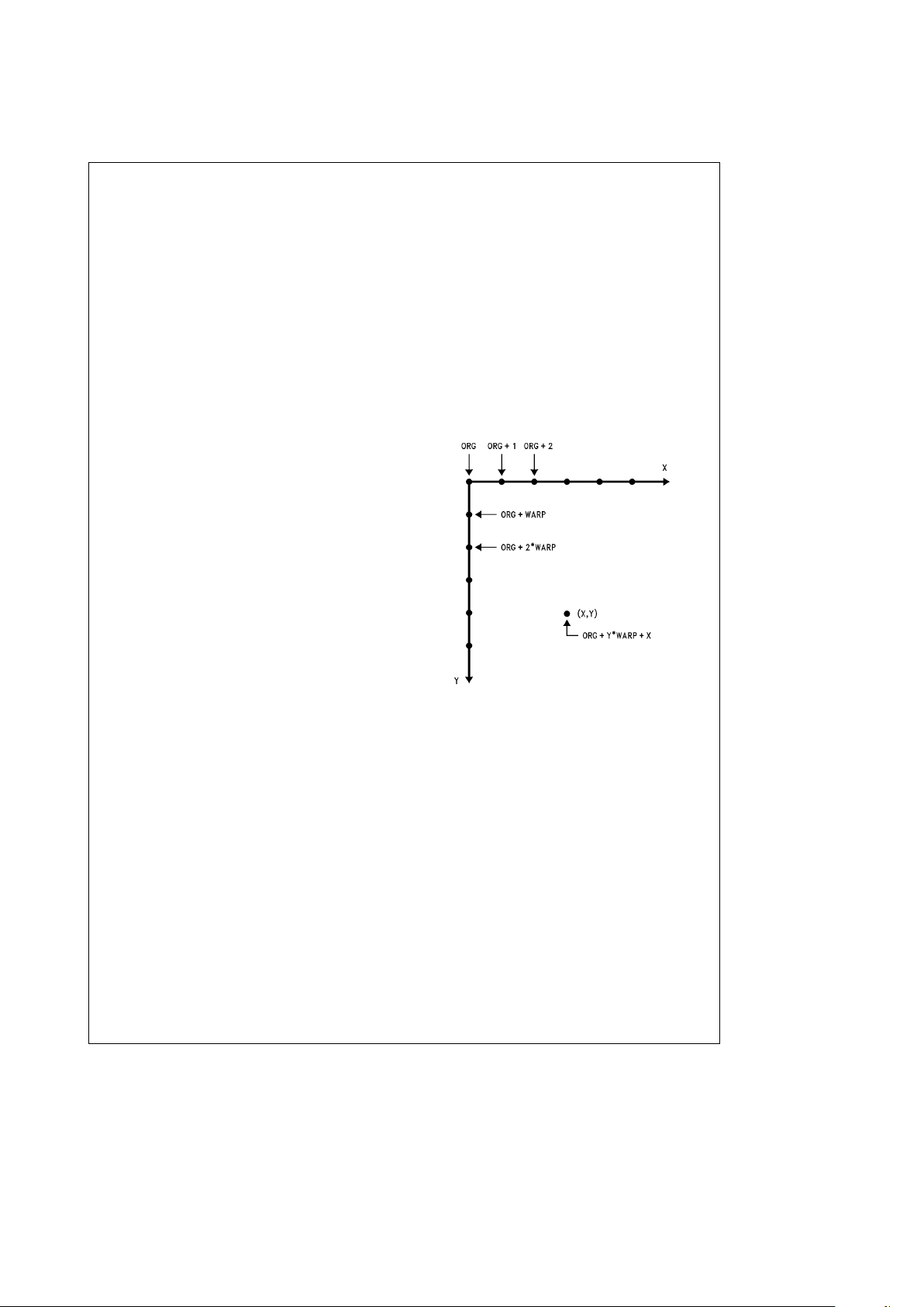
2.5.1 Frame Buffer Addressing
There are two basic addressing schemes for referencing
pixels within the frame buffer: Linear and Cartesian (or x-y).
Linear addressing associates a single number to each pixel
representing the physical address of the corresponding bit
in memory. Cartesian addressing associates two numbers
to each pixel representing the x and y coordinates of the
pixel relative to a point in the Cartesian space taken as the
origin. The Cartesian space is generally defined as having
the origin in the upper left. A movement to the right increases the x coordinate; a movement downward increases the y
coordinate.
The correspondence between the location of a pixel in the
Cartesian space and the physical (BIT) address in memory
is shown in
Figure 2-20
. The origin of the Cartesian space
(x
e
0, ye0) corresponds to the bit address ‘ORG’. Incrementing the x coordinate increments the bit address by one.
Incrementing the y coordinate increments the bit address by
an amount representing the warp (or pitch) of the Cartesian
space. Thus, the linear address of a pixel at location (x, y) in
the Cartesian space can be found by the following expression.
ADDR
e
ORGay * WARPax
Warp is the distance (in bits) in the physical memory space
between two vertically adjacent bits in the Cartesian space.
Example 1 below shows two NS32FX164 instruction sequences to set a single pixel given the x and y coordinates.
Example 2 shows how to create a fat pixel by setting four
adjacent bits in the Cartesian space.
Example 1: Set pixel at location (x, y)
Setup: R0 x coordinate
R1 y coordinate
Instruction Sequence 1:
MULD WARP, R1 ; Y*WARP
ADDD R0, R1 ; 0 X 4 BIT OFFSET
SBITD R1, ORG ; SET PIXEL
Instruction Sequence 2:
INDEXD R1, (WARP-1), R0 ; Y*WARP 0 X
SBITD R1, ORG ; SET PIXEL
Example 2: Create fat pixel by setting bits at locations
(x, y), (x
a
1, y), (x, ya1) and (xa1, ya1).
Setup: R0 x coordinate
R1 y coordinate
Instruction Sequence:
INDEXD R1, (WARP-1), R0 ; BIT ADDRESS
SBITD 41, ORG ; SET FIRST PIXEL
ADDQD 1, R1 ; (X01, Y)
SBITD R1, ORG ; SECOND PIXEL
ADDD (WARP-1), R1 ; (X, Y01)
SBITD R1, ORG ; THIRD PIXEL
ADDQD 1, R1 ; (X01, Y01)
SBITD R1, ORG ; LAST PIXEL
TL/EE/11267– 6
FIGURE 2-20. Correspondence between
Linear and Cartesian Addressing
2.5.2 BITBLT Fundamentals
BITBLT, BIT-aligned BLock Transfer, is a general operator
that provides a mechanism to move an arbitrary size rectangle of an image from one part of the frame buffer to another.
During the data transfer process a bitwise logical operation
can be performed between the source and the destination
data. BITBLT is also called RasterOp: operations on rasters.
It defines two rectangular areas, source and destination,
and performs a logical operation (e.g., AND, OR, XOR) between these two areas and stores the result back to the
destination. It can be expressed in simple notation as:
Source op Destination
x
Destination
op: AND, OR, XOR, etc.
20
Page 21
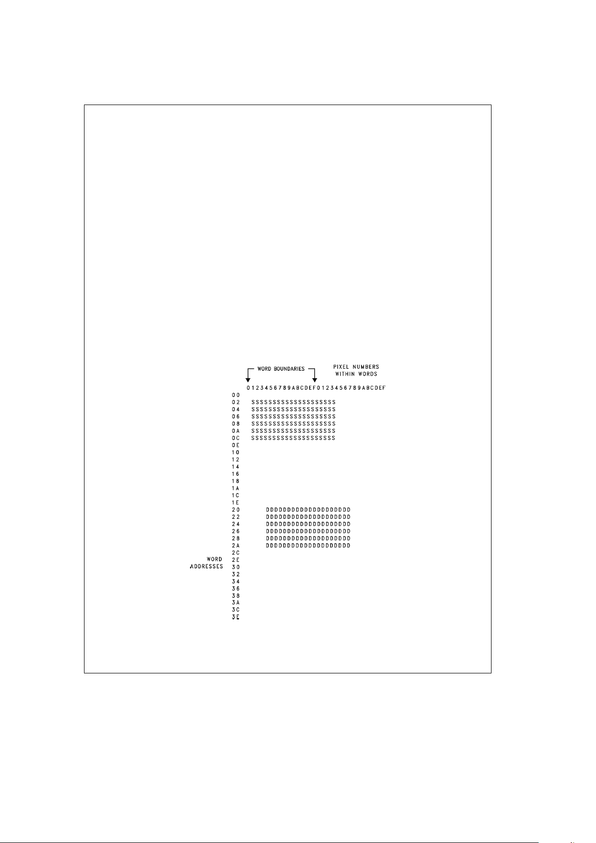
2.0 Architectural Description (Continued)
2.5.2.1 Frame Buffer Architecture
There are two basic types of frame buffer architectures:
plane-oriented or pixel-oriented. BITBLT takes advantage of
the plane-oriented frame buffer architecture’s attribute of
multiple, adjacent pixels-per-word, facilitating the movement
of large blocks of data. The source and destination starting
addresses are expressed as pixel addresses. The width and
height of the block to be moved are expressed in terms of
pixels and scan lines. The source block may start and end
at any bit position of any word, and the same applies for the
destination block.
2.5.2.2 Bit Alignment
Before a logical operation can be performed between the
source and the destination data, the source data must first
be bit aligned to the destination data. In
Figure 2-21
, the
source data needs to be shifted three bits to the right in
order to align the first pixel (i.e., the pixel at the top left
corner) in the source data block to the first pixel in the destination data block.
2.5.2.3 Block Boundaries and Destination Masks
Each BITBLT destination scan line may start and end at any
bit position in any data word. The neighboring bits (bits sharing the same word address with any words in the destination
data block, but not a part of the BITBLT rectangle) of the
BITBLT destination scan line must remain unchanged after
the BITBLT operation.
Due to the plane-oriented frame buffer architecture, all
memory operations must be word-aligned. In order to preserve the neighboring bits surrounding the BITBLT destination block, both a left mask and a right mask are needed for
all the leftmost and all the rightmost data words of the destination block. The left mask and the right mask both remain
the same during a BITBLT operation.
The following example illustrates the bit alignment requirements. In this example, the memory data path is 16 bits
wide.
Figure 2-21
shows a 32 pixel by 32 scan line frame
buffer which is organized as a long bit stream which wraps
around every two words (32 bits). The origin (top left corner)
of the frame buffer starts from the lowest word in memory
(word address 00 (hex)).
Each word in the memory contains 16 bits, D0 – D15. The
least significant bit of a memory word, D0, is defined as the
first displayed pixel in a word. In this example, BITBLT addresses are expressed as pixel addresses relative to the
origin of the frame buffer. The source block starting address
is 021 (hex) (the second pixel in the third word). The destination block starting address is 204 (hex) (the fifth pixel in
the 33rd word). The block width is 13 (hex), and the height is
06 (hex) (corresponding to 6 scan lines). The shift value is 3.
TL/EE/11267– 7
FIGURE 2-21. 32-Pixel by 32-Scan Line Frame Buffer
21
Page 22
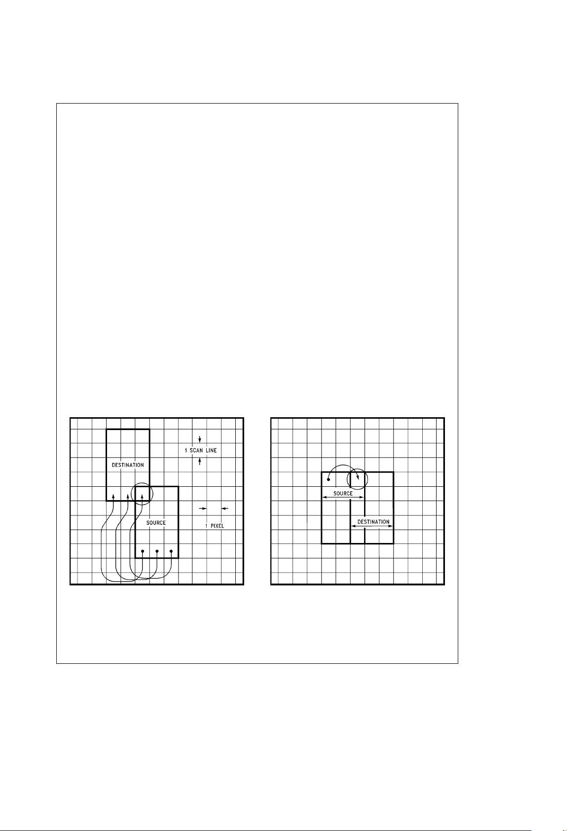
2.0 Architectural Description (Continued)
2.5.2.4 BITBLT Directions
A BITBLT operation moves a rectangular block of data in a
frame buffer. The operation itself can be considered as a
subroutine with two nested loops. The loops are preceded
by setup operations. In the outer loop the source and destination starting addresses are calculated, and the test for
completion is performed. In the inner loop the actual data
movement for a single scan line takes place. The length of
the inner loop is the number of (aligned) words spanned by
each scan line. The length of the outer loop is equal to the
height (number of scan lines) of the block to be moved. A
skeleton of the subroutine representing the BITBLT operation follows.
BITBLT: calculate BITBLT setup parameters;
(once per BITBLT operation).
such as
width, height
bit misalignment (shift number)
left, right masks
horizontal, vertical directions
etc
#
#
OUTERLOOP: calculate source, dest addresses;
(once per scanline).
INNERLOOP: move data, (logical operation) and incre-
ment addresses;
(once per word).
UNTIL done horizontally
UNTIL done vertically
RETURN (from BITBLT).
Note: In the NS32FX164 only the setup operations must be done by the
programmer. The inner and outer loops are automatically executed
by the BITBLT instructions.
Each loop can be executed in one of two directions: the
inner loop from left to right or right to left, the outer loop
from top to bottom (down) or bottom to top (up).
The ability to move data starting from any corner of the
BITBLT rectangle is necessary to avoid destroying the
BITBLT source data as a result of destination writes when
the source and destination are overlapped (i.e., when they
share pixels). This situation is routinely encountered while
panning or scrolling.
A determination of the correct execution directions of the
BITBLT must be performed whenever the source and destination rectangles overlap. Any overlap will result in the destruction of source data (from a destination write) if the correct vertical direction is not used. Horizontal BITBLT direction is of concern only in certain cases of overlap, as will be
explained below.
Figures 2-22(a)
and
(b)
illustrate two cases of overlap. Here,
the BITBLT rectangles are three pixels wide by five scan
lines high; they overlap by a single pixel in
(a)
and a single
column of pixels in
(b)
. For purposes of illustration, the
BITBLT is assumed to be carried out pixel-by-pixel. This
convention does not affect the conclusions.
In
Figure 2-22(a)
, if the BITBLT is performed in the UP direction (bottom-to-top) one of the transfers of the bottom scan
line of the source will write to the circled pixel of the destination. Due to the overlap, this pixel is also part of the uppermost scan line of the source rectangle. Thus, data needed
later is destroyed. Therefore, this BITBLT must be performed in the DOWN direction. Another example of this oc-
TL/EE/11267– 8
(a)
TL/EE/11267– 9
(b)
FIGURE 2-22. Overlapping BITBLT Blocks
The left mask and the right mask are 0000,1111,1111,1111 and 1111,1111,0000,0000 respectively.
Note 1: Zeros in either the left mask or the right mask indicate the destination bits which will not be modified.
Note 2: The BB(function) and EXTBLT instructions use different set up parameters, and techniques.
22
Page 23
2.0 Architectural Description (Continued)
curs any time the screen is moved in a purely vertical direction, as in scrolling text. It should be noted that, in both of
these cases, the choice of horizontal BITBLT direction may
be made arbitrarily.
Figure 2-22(b)
demonstrates a case in which the horizontal
BITBLT direction may not be chosen arbitrarily. This is an
instance of purely horizontal movement of data (panning).
Because the movement from source to destination involves
data within the same scan line, the incorrect direction of
movement will overwrite data which will be needed later. In
this example, the correct direction is from right to left.
2.5.2.5 BITBLT Variations
The ‘‘classical’’ definition of BITBLT, as described in
‘‘Smalltalk-80 The Language and its Implementation’’, by
Adele Goldberg and David Robson, provides for three operands: source, destination and mask/texture. This third operand is commonly used in monochrome systems to incorporate a stipple pattern into an area. These stipple patterns
provide the appearance of multiple shades of gray in singlebit-per-pixel systems, in a manner similar to the ‘‘halftone’’
process used in printing.
Texture op1 Source op2 Destination
x
Destination
While the NS32FX164 and the external BPU (if used) are
essentially two-operand devices, three-operand BITBLT operations can be implemented quite flexibly and efficiently by
performing the two operations serially.
2.5.3 GRAPHICS SUPPORT INSTRUCTIONS
The NS32FX164 provides eleven instructions for supporting
graphics oriented applications. These instructions are divided into three groups according to the operations they perform. General descriptions for each of them and the related
formats are provided in the following sections.
2.5.3.1 BITBLT (BIT-aligned BLock Transfer)
This group includes seven instructions. They are used to
move characters and objects into the frame buffer which will
be printed or displayed. One of the instructions works in
conjunction with an external BITBLT Processing Unit (BPU)
to maximize performance. The other six are executed by the
NS32FX164.
BIT-aligned BLock Transfer
Syntax: BB(function) Options
Setup: R0 base address, source data
R1 base address, destination data
R2 shift value
R3 height (in lines)
R4 first mask
R5 second mask
R6 source warp (adjusted)
R7 destination warp (adjusted)
0(SP) width (in words)
Function: AND, OR, XOR, FOR, STOD
Options: IA Increasing Address (default option).
When IA is selected, scan lines are
transferred in the increasing BIT/BYTE
order.
DA Decreasing Address.
S True Source (default option).
b
S Inverted Source.
These five instructions perform standard BITBLT operations
between source and destination blocks. The operations
available include the following:
BBAND: src AND dst
b
src AND dst
BBOR: src OR dst
b
src OR dst
BBXOR: src XOR dst
b
src XOR dst
BBFOR: src OR dst
BBSTOD: src TO dst
b
src TO dst
‘src’ and ‘
b
src’ stand for ‘True Source’ and ‘Inverted
Source’ respectively; ‘dst’ stands for ‘Destination’.
Note 1: For speed reasons, the BB instructions require the masks to be
specified with respect to the source block. In
Figure 2-21
masking
was defined relative to the destination block.
Note 2: The options
b
S and DA are not available for the BBFOR instruc-
tion.
Note 3: BBFOR performs the same operation as BBOR with IA and S op-
tions.
Note 4: IA and DA are mutually exclusive and so are S and
b
S.
Note 5: The width is defined as the number of words of source data to read.
Note 6: An odd number of bytes can be specified for the source warp.
However, word alignment of source scan lines will result in faster
execution.
The horizontal and vertical directions of the BITBLT operations performed by the above instructions, with the exception of BBFOR, are both programmable. The horizontal direction is controlled by the IA and DA options. The vertical
direction is controlled by the sign of the source and destination warps.
Figure 2-23
and Table 2-3 show the format of
the BB instructions and the encodings for the ‘op’ and ‘i’
fields.
23 16 15 8 7 0
000 000 D X S 0 op i 00001110
#
D is set when the DA option is selected
#
S is set when thebS option is selected
#
X is set for BBAND, and it is clear for all other BB instructions
FIGURE 2-23. BB Instructions Format
TABLE 2-3. ‘op’ and ‘i’ Field Encodings
Instruction Options ‘op’ Field ‘i’ Field
BBAND Yes 1010 11
BBOR Yes 0110 01
BBXOR Yes 1110 01
BBFOR No 1100 01
BBSTOD Yes 0100 01
BIT-aligned Word Transfer
Syntax: BITWT
Setup: R0 Base address, source word
R1 Base address, destination double word
R2 Shift value
The BITWT instruction performs a fast logical OR operation
between a source word and a destination double word,
stores the result into the destination double word and increments registers R0 and R1 by two. Before performing the
OR operation, the source word is shifted left (i.e., in the
direction of increasing bit numbers) by the value in register
R2.
23
Page 24
2.0 Architectural Description (Continued)
This instruction can be used within the inner loop of a block
OR operation. Its use assumes that the source data is
‘clean’ and does not need masking. The BITWT format is
shown in
Figure 2-24
.
23 16 15 8 7 0
0000000000100001 0 000 1110
FIGURE 2-24. BITWT Instruction Format
External BITBLT
Syntax: EXTBLT
Setup: R0 base addresses, source data
R1 base address, destination data
R2 width (in bytes)
R3 height (in lines)
R4 horizontal increment/decrement
R5 temporary register (current width)
R6 source warp (adjusted)
R7 destination warp (adjusted)
Note 1: R0 and R1 are updated after execution to point to the last source
and destination addresses plus related warps. R2, R3 and R5 will
be modified. R4, R6, and R7 are returned unchanged.
Note 2: Source and destination pointers should point to word-aligned oper-
ands to maximize speed and minimize external interface logic.
This instruction performs an entire BITBLT operation in conjunction with an external BITBLT Processing Unit (BPU).
The external BPU Control Register should be loaded by the
software before the instruction is executed (refer to the
DP8510 or DP8511 data sheets for more information on the
BPU). The NS32FX164 generates a series of source read,
destination read and destination write bus cycles until the
entire data block has been transferred. The BITBLT operation can be performed in either horizontal direction. As controlled by the sign of the contents of register R4.
Depending on the relative alignment of the source and destination blocks, an extra source read may be required at the
beginning of each scan line, to load the pipeline register in
the external BPU. The L bit in the PSR register determines
whether the extra source read is performed. If L is 1, no
extra read is performed. The instructions CMPQB 2,1 or
CMPQB 1,2 could be executed to provide the right setting
for the L bit just before executing EXTBLT.
Figure 2-25
shows the EXTBLT format. The bus activity for a simple
BITBLT operation is shown in
Figure 2-30.
23 15 8 7 0
000000000001011100001110
FIGURE 2-25. EXTBLT Instruction Format
2.5.3.2 Pattern Fill
Only one instruction is in this group. It is usually used for
clearing RAM and drawing patterns and lines.
Move Multiple Pattern
Syntax: MOVMPi
Setup: R0 base address of the destination
R1 pointer increment (in bytes)
R2 number of pattern moves
R3 source pattern
Note: R1 and R3 are not modified by the instruction. R2 will always be
returned as zero. R0 is modified to reflect the last address into which
a pattern was written.
This instruction stores the pattern in register R3 into the
destination area whose address is in register R0. The pattern count is specified in register R2. After each store operation the destination address is changed by the contents of
register R1. This allows the pattern to be stored in rows, in
columns, and in any direction, depending on the value and
sign of R1. The MOVMPi instruction format is shown in
Fig-
ure 2-26
.
23 15 8 7 0
00000000000111 i 00001110
FIGURE 2-26. MOVMPi Instruction Format
2.5.3.3 Data Compression, Expansion and Magnify
The three instructions in this group can be used to compress data and restore data from compression. A compressed character set may require from 30% to 50% less
memory space for its storage.
The compression ratio possible can be 50:1 or higher depending on the data and algorithm used. TBITS can also be
used to find boundaries of an object. As a character is needed, the data is expanded and stored in a RAM buffer. The
expand instructions (SBITS, SBITPS) can also function as
line drawing instructions.
Test Bit String
Syntax: TBITS option
Setup: R0 base address, source (byte address)
R1 starting source bit offset
R2 destination run length limited code
R3 maximum value run length limit
R4 maximum source bit offset
Option: 1 count set bits until a clear bit is found
0 count clear bits until a set bit is found
Note: R0, R3 and R4 are not modified by the instruction execution. R1
reflects the new bit offset. R2 holds the result.
This instruction starts at the base address, adds a bit offset,
and tests the bit for clear if ‘‘option’’
e
0 (and for set if
‘‘option’’
e
1). If clear (or set), the instruction increments to
the next higher bit and tests for clear (or set). This testing
for clear proceeds through memory until a set bit is found or
until the maximum source bit offset or maximum run length
value is reached. The total number of clear bits is stored in
the destination as a run length value.
When TBITS finds a set bit and terminates, the bit offset is
adjusted to reflect the current bit address. Offset is then
ready for the next TBITS instruction with ‘‘option’’
e
0. After
the instruction is executed, the F flag is set to the value of
the bit previous to the bit currently being pointed to (i.e., the
value of the bit on which the instruction completed execution). In the case of a starting bit offset exceeding the maximum bit offset (R1
t
R4), the F flag is set if the option was
1 and clear if the option was 0. The L flag is set when the
desired bit is found, or if the run length equalled the maximum run length value and the bit was not found. It is cleared
otherwise.
Figure 2-27
shows the TBITS instruction format.
23 15 8 7 0
00000000S010011100001110
#
S is set for ‘TBITS 1’ and clear for ‘TBITS 0’.
FIGURE 2-27. TBITS Instruction Format
24
Page 25
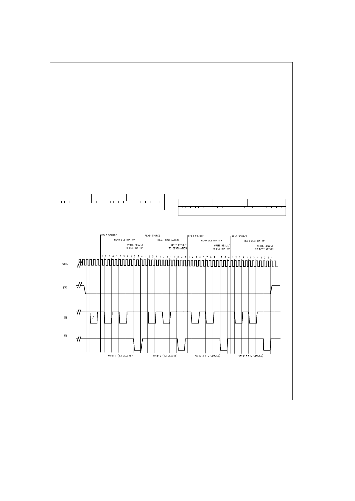
2.0 Architectural Description (Continued)
Set Bit String
Syntax: SBITS
Setup: R0 base address of the destination
R1 starting bit offset (signed)
R2 number of bits to set (unsigned)
R3 address of string look-up table
Note: When the instruction terminates, the registers are returned un-
changed.
SBITS sets a number of contiguous bits in memory to 1, and
is typically used for data expansion operations. The instruction draws the number of ones specified by the value in R2,
starting at the bit address provided by registers R0 and R1.
In order to maximize speed and allow drawing of patterned
lines, an external 1k byte lookup table is used. The lookup
table is specified in the NS32CG16 Printer/Display Processor Programmer’s Reference Supplement.
When SBITS begins executing, it compares the value in R2
with 25. If the value in R2 is less than or equal to 25, the F
flag is cleared and the appropriate number of bits are set in
memory. If R2 is greater than 25, the F flag is set and no
other action is performed. This allows the software to use a
faster algorithm to set longer strings of bits.
Figure 2-28
shows the SBITS instruction format.
23 15 8 7 0
000000000011011100001110
FIGURE 2-28. SBITS Instruction Format
Set BIT Perpendicular String
Syntax: SBITPS
Setup: R0 base address, destination (byte address)
R1 starting bit offset
R2 number of bits to set
R3 destination warp (signed value, in bits)
Note: When the instruction terminates, the R0 and R3 registers are re-
turned unchanged. R1 becomes the final bit offset. R2 is zero.
The SBITPS can be used to set a string of bits in any direction. This allows a font to be expanded with a 90 or 270
degree rotation, as may be required in a printer application.
SBITPS sets a string of bits starting at the bit address specified in registers R0 and R1. The number of bits in the string
is specified in R2. After the first bit is set, the destination
warp is added to the bit address and the next bit is set. The
process is repeated until all the bits have been set. A negative raster warp offset value leads to a 90 degree rotation. A
positive raster warp value leads to a 270 degree rotation. If
the R3 value is
e
(space warpa1orb1), then the result is
a 45 degree line. If the R3 value is
a
1orb1, a horizontal
line results.
SBITS and SBITPS allow expansion on any 90 degree angle, giving portrait, landscape and mirror images from one
font.
Figure 2-29
shows the SBITPS instruction format.
23 15 8 7 0
000000000010111100001110
FIGURE 2-29. SBITPS Instruction Format
TL/EE/11267– 10
FIGURE 2-30. Bus Activity for a Simple BITBLT Operation
Note 1: This example is for a block 4 words wide and 1 line high.
Note 2: The sequence is common with all logical operations of the DP8510/DP8511 BPU.
Note 3: Mask values, shift values and number of bit planes do not affect the performance.
Note 4: Zero wait states are assumed throughout the BITBLT operation.
Note 5: The extra read is performed when the BPU pipeline register needs to be preloaded.
25
Page 26
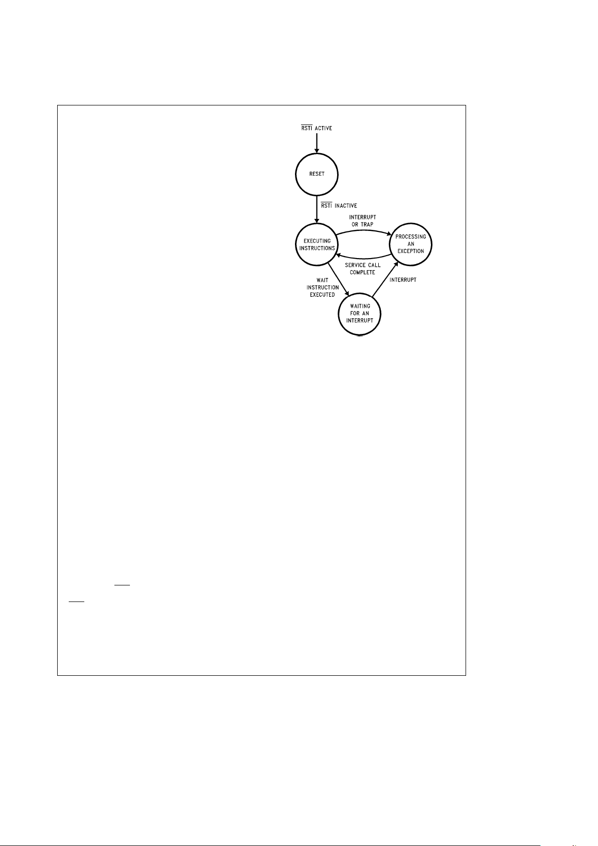
2.0 Architectural Description (Continued)
2.5.3.3.1 Magnifying Compressed Data
Restoring data is just one application of the SBITS and
SBITPS instructions. Multiplying the ‘‘length’’ operand used
by the SBITS and SBITPS instructions causes the resulting
pattern to be wider, or a multiple of ‘‘length’’.
As the pattern of data is expanded, it can be magnified by
2x, 3x, 4x, . . . , 10x and so on. This creates several sizes of
the same style of character, or changes the size of a logo. A
magnify in both dimensions X and Y can be accomplished
by drawing a single line, then using the MOVS (Move String)
or the BB instructions to duplicate the line, maintaining an
equal aspect ratio.
More information on this subject is provided in the
NS32CG16 Printer/Display Processor Programmer’s Reference Supplement.
3.0 Functional Description
This chapter provides details on the functional characteristics of the NS32FX164 microprocessor.
The chapter is divided into five main sections:
Instruction Execution, Exception Processing, Debugging,
DSP Module and System Interface.
3.1 INSTRUCTION EXECUTION
To execute an instruction, the NS32FX164 performs the following operations:
#
Fetch the Instruction
#
Read Source Operands, if Any (1)
#
Calculate Results
#
Write Result Operands, if Any
#
Modify Flags, if Necessary
#
Update the Program Counter
Under most circumstances, the CPU can be conceived to
execute instructions by completing the operations above in
strict sequence for one instruction and then beginning the
sequence of operations for the next instruction. However,
due to the internal instruction pipelining, as well as the occurrence of exceptions, the sequence of operations performed during the execution of an instruction may be altered. Furthermore, exceptions also break the sequentiality
of the instructions executed by the CPU.
Note 1: In this and following sections, memory locations read by the CPU to
calculate effective addresses for Memory-Relative and External addressing modes are considered like source operands, even if the
effective address is being calculated for an operand with access
class of write.
3.1.1 Operating States
The CPU has four operating states regarding the execution
of instructions and the processing of exceptions: Reset, Executing Instructions, Processing An Exception and WaitingFor-An-Interrupt. The various states and transitions between them are shown in
Figure 3-1
.
Whenever the RSTI signal is asserted, the CPU enters the
reset state. The CPU remains in the reset state until the
RSTI
signal is driven inactive, at which time it enters the
Executing-Instructions state. In the Reset state the contents
of certain registers are initialized. Refer to Section 3.5.4 for
details.
TL/EE/11267– 11
FIGURE 3-1. Operating States
In the Executing-Instructions state, the CPU executes instructions. It will exit this state when an exception is recognized or a WAIT instruction is encountered. At which time it
enters the Processing-An-Exception state or the WaitingFor-An-Interrupt state respectively.
While in the Processing-An-Exception state, the CPU saves
the PC, PSR and MOD register contents on the stack and
reads the new PC and module linkage information to begin
execution of the exception service procedure.
Following the completion of all data references required to
process an exception, the CPU enters the Executing-Instructions state.
In the Waiting-For-An-Interrupt state, the CPU is idle. A special status identifying this state is presented on the system
interface (Section 3.5). When an interrupt is detected, the
CPU enters the Processing-An-Exception State.
3.1.2 Instruction Endings
The NS32FX164 checks for exceptions at various points
while executing instructions. Certain exceptions, like interrupts, are in most cases recognized between instructions.
Other exceptions, like Divide-By-Zero Trap, are recognized
during execution of an instruction. When an exception is
recognized during execution of an instruction, the instruction
ends in one of four possible ways: completed, suspended,
terminated, or partially completed. Each type of exception
causes a particular ending, as specified in Section 3.2.
26
Page 27

3.0 Functional Description (Continued)
3.1.2.1 Completed Instructions
When an exception is recognized after an instruction is
completed, the CPU has performed all of the operations for
that instruction and for all other instructions executed since
the last exception occurred. Result operands have been
written, flags have been modified, and the PC saved on the
Interrupt Stack contains the address of the next instruction
to execute. The exception service procedure can, at its conclusion, execute the RETT instruction (or the RETI instruction for maskable interrupts), and the CPU will begin executing the instruction following the completed instruction.
3.1.2.2 Suspended Instructions
An instruction is suspended when one of several trap conditions is detected during execution of the instruction. A suspended instruction has not been completed, but all other
instructions executed since the last exception occurred
have been completed. Result operands and flags due to be
affected by the instruction may have been modified, but only
modifications that allow the instruction to be executed again
and completed can occur. For certain exceptions (Trap
(UND) the CPU clears the P-flag in the PSR before saving
the copy that is pushed on the Interrupt Stack. The PC
saved on the Interrupt Stack contains the address of the
suspended instruction.
To complete a suspended instruction, the exception service
procedure takes either of two actions:
1. The service procedure can simulate the suspended instruction’s execution. After calculating and writing the instruction’s results, the flags in the PSR copy saved on the
Interrupt Stack should be modified, and the PC saved on
the Interrupt Stack should be updated to point to the next
instruction to execute. The service procedure can then
execute the RETT instruction, and the CPU begins executing the instruction following the suspended instruction.
This is the action taken when floating-point instructions
are simulated by software in systems without a hardware
floating-point unit.
2. The suspended instruction can be executed again after
the service procedure has eliminated the trap condition
that caused the instruction to be suspended. The service
procedure should execute the RETT instruction at its conclusion; then the CPU begins executing the suspended
instruction again. This is the action taken by a debugger
when it encounters a BPT instruction that was temporarily
placed in another instruction’s location in order to set a
breakpoint.
Note 1: It may be necessary for the exception service procedure to alter the
P-flag in the PSR copy saved on the Interrupt Stack: If the exception
service procedure simulates the suspended instruction and the Pflag was cleared by the CPU before saving the PSR copy, then the
saved T-flag must be copied to the saved P-flag (like the floatingpoint instruction simulation described above). Or if the exception
service procedure executes the suspended instruction again and
the P-flag was not cleared by the CPU before saving the PSR copy,
then the saved P-flag must be cleared (like the breakpoint trap described above). Otherwise, no alteration to the saved P-flag is necessary.
3.1.2.3 Terminated Instructions
An instruction being executed is terminated when reset occurs. Any result operands and flags due to be affected by
the instruction are undefined, as is the contents of the PC.
3.1.2.4 Partially Completed Instructions
When an interrupt condition is recognized during execution
of a string instruction, the instruction is said to be partially
completed. A partially completed instruction has not completed, but all other instructions executed since the last exception occurred have been completed. Result operands
and flags due to be affected by the instruction may have
been modified, but the values stored in the string pointers
and other general-purpose registers used during the instruction’s execution allow the instruction to be executed again
and completed.
The CPU clears the P-flag in the PSR before saving the
copy that is pushed on the Interrupt Stack. The PC saved on
the Interrupt Stack contains the address of the partially
completed instruction. The exception service procedure
can, at its conclusion, simply execute the RETT instruction
(or the RETI instruction for maskable interrupts), and the
CPU will resume executing the partially completed instruction.
3.1.3 Slave Processor Instructions
The NS32FX164 supports only one group of instructions,
the floating-point instruction set, as being executable by a
slave processor. The floating-point instruction set is validated by the F-bit in the CFG register.
If a floating-point instruction is encountered and the F-bit in
the CFG register is not set, a Trap (UND) will result, without
any slave processor communication attempted by the CPU.
This allows software emulation in case an external floatingpoint unit (FPU) is not used.
3.1.3.1 Slave Processor Protocol
Slave Processor instructions have a three-byte Basic Instruction field, consisting of an ID Byte followed by an Operation Word. The ID Byte has three functions:
1. It identifies the instruction as being a Slave Processor
instruction.
2. It specifies which Slave Processor will execute it.
3. It determines the format of the following Operation Word
of the instruction.
Upon receiving a Slave Processor instruction, the CPU initiates the sequence outlined in
Figure 3-2
. While applying
Status Code 1111 (Broadcast ID, Section 3.5.5.1), the CPU
transfers the ID Byte on the least-significant half of the Data
Bus (AD0 – AD7). All Slave Processors input this byte and
decode it. The Slave Processor selected by the ID Byte is
activated, and from this point the CPU is communicating
only with it. If any other slave protocol was in progress (e.g.,
an aborted Slave instruction), this transfer cancels it.
27
Page 28

3.0 Functional Description (Continued)
The CPU next sends the Operation Word while applying
Status Code 1101 (Transfer Slave Operand, Section
3.5.5.1). Upon receiving it, the Slave Processor decodes it,
and at this point both the CPU and the Slave Processor are
aware of the number of operands to be transferred and their
sizes. The Operation Word is swapped on the Data Bus;
that is, bits 0–7 appear on pins AD8 – AD15 and bits 8 – 15
appear on pins AD0 –AD7.
Using the Address Mode fields within the Operation Word,
the CPU starts fetching operands and issuing them to the
Slave Processor. To do so, it references any Addressing
Mode extensions which may be appended to the Slave
Processor instruction. Since the CPU is solely responsible
for memory accesses, these extensions are not sent to the
Slave Processor. The Status Code applied is 1101 (Transfer
Slave Processor Operand, Section 3.5.5.1).
After the CPU has issued the last operand, the Slave Processor starts the actual execution of the instruction. Upon
completion, it will signal the CPU by pulsing SPC
low.
While the Slave Processor is executing the instruction, the
CPU is free to prefetch instructions into its queue. If it fills
the queue before the Slave Processor finishes, the CPU will
wait, applying Status Code 0011 (Waiting for Slave).
Upon receiving the pulse on SPC
, the CPU uses SPC to
read a Status Word from the Slave Processor, applying
Status Code 1110 (Read Slave Status). This word has the
format shown in
Figure 3-3
. If the Q-bit (‘‘Quit’’, Bit 0) is set,
this indicates that an error was detected by the Slave Processor. The CPU will not continue the protocol, but will imme-
Status Combinations:
Send ID (ID): Code 1111
Xfer Operand (OP): Code 1101
Read Status (ST): Code 1110
Step Status Action
1 ID CPU Sends ID Byte
2 OP CPU Sends Operation Word
3 OP CPU Sends Required Operands
4 Ð Slave Starts Execution.
CPU Pre-Fetches.
5 Ð Slave Pulses SPC
Low
6 ST CPU Reads Status Word.
(Trap? Alter Flags?)
7 OP CPU Reads Results (If Any).
FIGURE 3-2. Slave Processor Protocol
diately trap through the Slave vector in the Interrupt Table.
Certain Slave Processor instructions cause CPU PSR bits to
be loaded from the Status Word.
The last step in the protocol is for the CPU to read a result,
if any, and transfer it to the destination. The Read cycles
from the Slave Processor are performed by the CPU while
applying Status Code 1101 (Transfer Slave Operand).
3.1.3.2 Floating-Point Instructions
Table 3-1 gives the protocols followed for each FloatingPoint instruction. The instructions are referenced by their
mnemonics. For the bit encodings of each instruction, see
Appendix A.
TABLE 3-1. Floating-Point Instruction Protocols
Mnemonic
Operand 1 Operand 2 Operand 1 Operand 2 Returned Value PSR Bits
Class Class Issued Issued Type and Dest. Affected
ADDf read.f rmw.f f f f to Op.2 none
SUBf read.f rmw.f f f f to Op.2 none
MULf read.f rmw.f f f f to Op.2 none
DIVf read.f rmw.f f f f to Op.2 none
MOVf read.f write.f f N/A f to Op.2 none
ABSf read.f write.f f N/A f to Op.2 none
NEGf read.f write.f f N/A f to Op.2 none
CMPf read.f read.f f f N/A N,Z,L
FLOORfi read.f write.i f N/A i to Op.2 none
TRUNCfi read.f write.i f N/A i to Op.2 none
ROUNDfi read.f write.i f N/A i to Op.2 none
MOVFL read.F write.L F N/A L to Op.2 none
MOVLF read.L write.F L N/A F to Op.2 none
MOVif read.i write.f i N/A f to Op.2 none
LFSR read.D N/A D N/A N/A none
SFSR N/A write.D N/A N/A D to Op. 2 none
POLYf read.f read.f f f f to F0 none
DOTf read.f read.f f f f to F0 none
SCALBf read.f rmw.f f f f to Op. 2 none
LOGBf read.f write.f f N/A f to Op. 2 none
Notes:
D
e
Double Word
i
e
Integer size (B, W, D) specified in mnemonic.
f
e
Floating-Point type (F, L) specified in mnemonic.
N/A
e
Not Applicable to this instruction.
28
Page 29
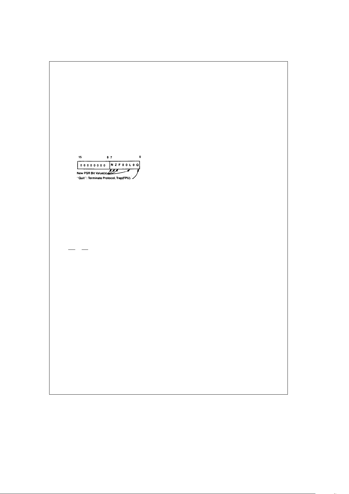
3.0 Functional Description (Continued)
The Operand class columns give the Access Class for each
general operand, defining how the addressing modes are
interpreted (see Series 32000 Instruction Set Reference
Manual).
The Operand Issued columns show the sizes of the operands issued to the Floating-Point Unit by the CPU. ‘‘D’’ indicates a 32-bit Double Word. ‘‘i’’ indicates that the instruction
specifies an integer size for the operand (B
e
Byte,
W
e
Word, DeDouble Word). ‘‘f’’ indicates that the instruction specifies a Floating-Point size for the operand
(F
e
32-bit Standard Floating, Le64-bit Long Floating).
The Returned Value Type and Destination column gives the
size of any returned value and where the CPU places it. The
PSR Bits Affected column indicates which PSR bits, if any,
are updated from the Slave Processor Status Word
(Figure
3-3)
.
TL/EE/11267– 12
FIGURE 3-3. Slave Processor Status Word
Any operand indicated as being of type ‘‘f’’ will not cause a
transfer if the Register addressing mode is specified. This is
because the Floating-Point Registers are physically on the
Floating-Point Unit and are therefore available without CPU
assistance.
3.2 EXCEPTION PROCESSING
Exceptions are special events that alter the sequence of
instruction execution. The CPU recognizes two basic types
of exceptions: interrupts and traps.
An interrupt occurs in response to an event generated either
internally, by the on-chip DSP Module, or externally, by activating NMI
or INT. External interrupts are typically request-
ed by peripheral devices that require the CPU’s attention.
Traps occur as a result either of exceptional conditions
(e.g., attempted division by zero) or of specific instructions
whose purpose is to cause a trap to occur (e.g., supervisor
call instruction).
When an exception is recognized, the CPU saves the PC,
PSR and optionally the MOD register contents on the interrupt stack and then it transfers control to an exception service procedure.
Details on the operations performed in the various cases by
the CPU to enter and exit the exception service procedure
are given in the following sections.
It is to be noted that the reset operation is not treated here
as an exception. Even though, like any exception, it alters
the instruction execution sequence.
The reason being that the CPU handles reset in a significantly different way than it does for exceptions.
Refer to Section 3.5.4 for details on the reset operation.
3.2.1 Exception Acknowledge Sequence
When an exception is recognized, the CPU goes through
three major steps:
1. Adjustment of Registers. Depending on the source of the
exception, the CPU may restore and/or adjust the contents of the Program Counter (PC), the Processor Status
Register (PSR) and the currently-selected Stack Pointer
(SP). A copy of the PSR is made, and the PSR is then set
to reflect Supervisor Mode and selection of the Interrupt
Stack. Trap (TRC) always disabled. Maskable interrupts
are also disabled if the exception is caused by an interrupt.
2. Vector Acquisition. A vector is either obtained from an
external interrupt control unit or is supplied internally by
default.
3. Service Call. The CPU performs one of two sequences
common to all exceptions to complete the acknowledge
process and enter the appropriate service procedure.
The selection between the two sequences depends on
whether the Direct-Exception mode is disabled or enabled.
Direct-Exception Mode Disabled
The Direct-Exception mode is disabled while the DE bit in
the CFG register is 0 (Section 2.1.4). In this case the CPU
first pushes the saved PSR copy along with the contents of
the MOD and PC registers on the interrupt stack. Then it
reads the double-word entry from the Interrupt Dispatch table at address ‘‘INTBASE’’
a
vectorc4’’. See
Figures 3-4
and
3-5
. The CPU uses this entry to call the exception service procedure, interpreting the entry as an external procedure descriptor.
A new module number is loaded into the MOD register from
the least-significant word of the descriptor, and the staticbase pointer for the new module is read from memory and
loaded into the SB register. Then the program-base pointer
for the new module is read from memory and added to the
most-significant word of the module descriptor, which is interpreted as an unsigned value. Finally, the result is loaded
into the PC register.
Direct-Exception Mode Enabled
The Direct-Exception mode is enabled when the DE bit in
the CFG register is set to 1. In this case the CPU first
pushes the saved PSR copy along with the contents of the
PC register on the Interrupt Stack. The word stored on the
Interrupt Stack between the saved PSR and PC register is
reserved for future use; its contents are undefined. The CPU
then reads the double-word entry from the Interrupt Dispatch Table at address ‘‘INTBASE
a
vectorc4’’. The
CPU uses this entry to call the exception service procedure,
interpreting the entry as an absolute address that is simply
loaded into the PC register.
Figure 3-6
provides a pictorial of
the acknowledge sequence. It is to be noted that while the
direct-exception mode is enabled, the CPU can respond
more quickly to interrupts and other exceptions because
fewer memory references are required to process an exception. The MOD and SB registers, however, are not initialized
before the CPU transfers control to the service procedure.
Consequently, the service procedure is restricted from executing any instructions, such as CXP, that use the contents
of the MOD or SB registers in effective address calculations.
29
Page 30
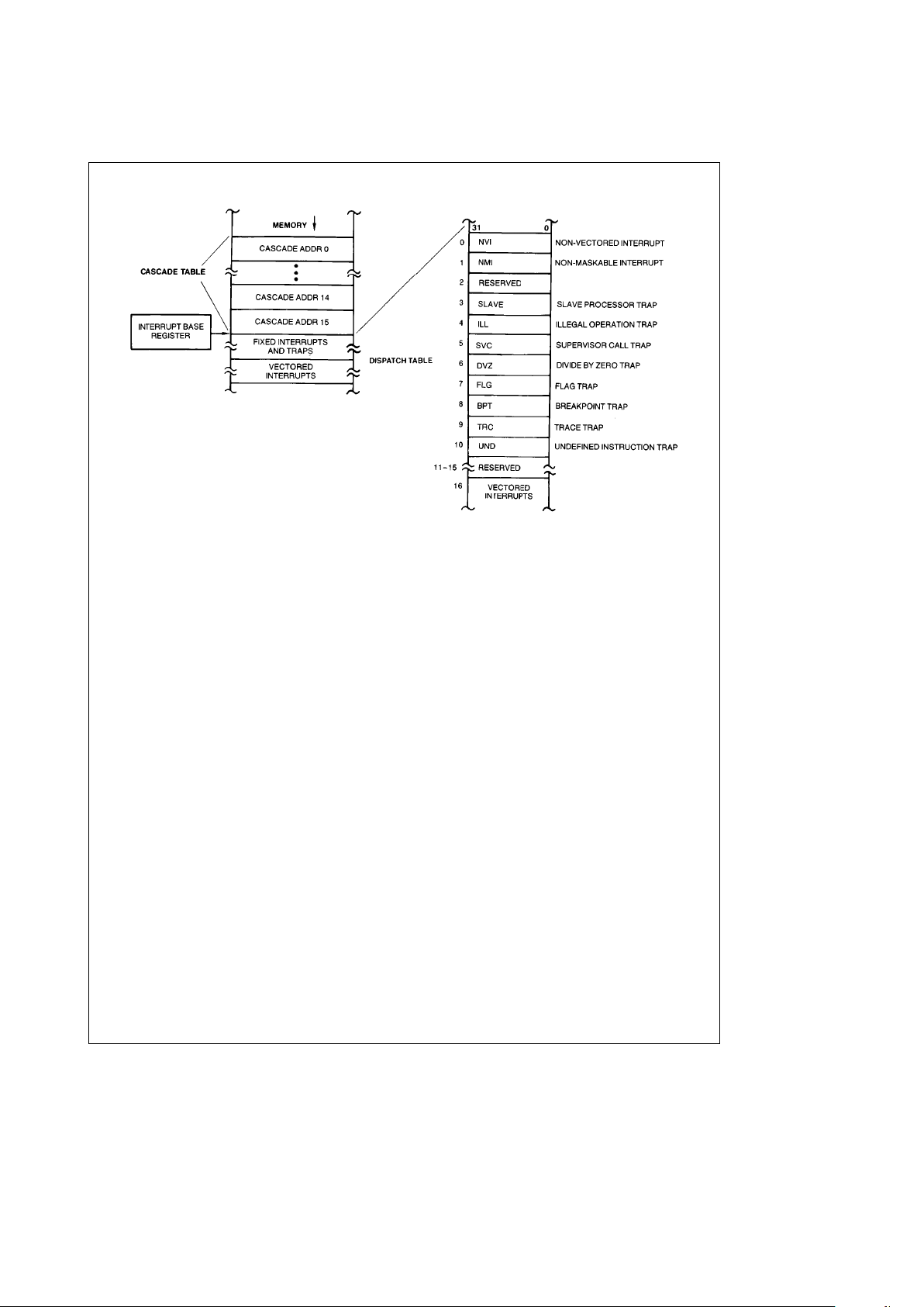
3.0 Functional Description (Continued)
TL/EE/11267– 13
FIGURE 3-4. Interrupt Dispatch and Cascade Tables
3.2.2 Returning from an Exception Service Procedure
To return control to an interrupted program, one of two instructions can be used: RETT (Return from Trap) and RETI
(Return from Interrupt).
RETT is used to return from any trap or non-maskable interrupt service procedure. Since some traps are often used
deliberately as a call mechanism for supervisor mode procedures, RETT can also adjust the Stack Pointer (SP) to discard a specified number of bytes from the original stack as
surplus parameter space.
RETI is used to return from a maskable interrupt service
procedure. A difference of RETT, RETI also informs the onchip ICU as well as any external interrupt control logic that
interrupt service has completed. Since interrupts are generally asynchronous external events, RETI does not discard
parameters from the stack.
Both of the above instructions always restore the Program
Counter (PC) and the Processor Status Register from the
interrupt stack. If the Direct-Exception mode is disabled,
they also restore the MOD and SB register contents.
Fig-
ures 3-7
and
3-8
show the RETT and RETI instruction flows
when the Direct-Exception mode is disabled.
30
Page 31

3.0 Functional Description (Continued)
TL/EE/11267– 16
TL/EE/11267– 17
FIGURE 3-5. Exception Acknowledge Sequence:
Direct-Exception Mode Disabled
31
Page 32

3.0 Functional Description (Continued)
TL/EE/11267– 18
TL/EE/11267– 19
FIGURE 3-6. Exception Acknowledge Sequence:
Direct-Exception Mode Enabled
32
Page 33

3.0 Functional Description (Continued)
TL/EE/11267– 20
FIGURE 3-7. Return from Trap (RETTn) Instruction Flow:
Direct-Exception Mode Disabled
33
Page 34

3.0 Functional Description (Continued)
TL/EE/11267– 21
FIGURE 3-8. Return from Interrupt (RETI) Instruction Flow:
Direct-Exception Mode Disabled
3.2.3 Maskable Interrupts
The INT
pin is a level-sensitive input. A continuous low level
is allowed for generating multiple interrupt requests. The input is maskable, and is therefore enabled to generate interrupt requests only while the Processor Status Register I bit
is set. The I bit is automatically cleared during service of an
INT
or NMI request, and is restored to its original setting
upon return from the interrupt service routine via the RETT
or RETI instruction.
The INT
pin may be configured via the SETCFG instruction
as either Non-Vectored (CFG Register bit I
e
0) or Vec-
tored (bit I
e
1).
3.2.3.1 Non-Vectored Mode
In the Non-Vectored mode, an interrupt request on the INT
pin will cause an Interrupt Acknowledge bus cycle, but the
CPU will ignore any value read from the bus and use instead
a default vector of zero. This mode is useful for small systems in which hardware interrupt prioritization is unnecessary.
34
Page 35
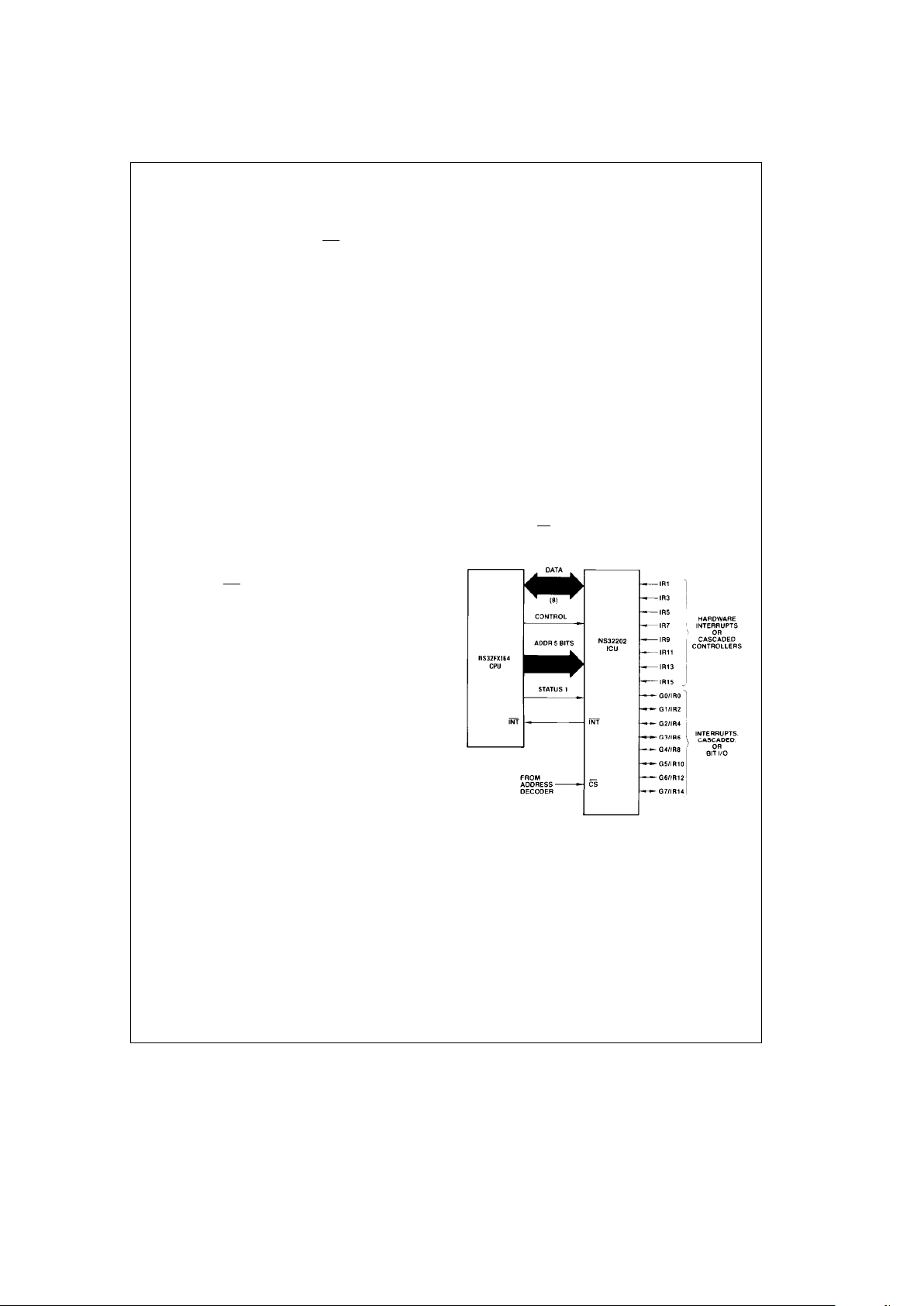
3.0 Functional Description (Continued)
3.2.3.2 Vectored Mode: Non-Cascaded Case
In the Vectored mode, the CPU uses an Interrupt Control
Unit (ICU) to prioritize up to 16 interrupt requests. Upon receipt of an interrupt request on the INT
pin, the CPU performs an ‘‘Interrupt Acknowledge, Master’’ bus cycle reading a vector value from the low-order byte of the Data Bus.
This vector is then used as an index into the Dispatch Table
in order to find the External Procedure Descriptor for the
proper interrupt service procedure. The service procedure
eventually returns via the Return from Interrupt (RETI) instruction, which performs an End of Interrupt bus cycle, informing the ICU that it may re-prioritize any interrupt requests still pending. The ICU provides the vector number
again, which the CPU uses to determine whether it needs
also to inform a Cascaded ICU.
In a system with only one ICU (16 levels of interrupt), the
vectors provided must be in the range of 0 through 127; that
is, they must be positive numbers in eight bits. By providing
a negative vector number, an ICU flags the interrupt source
as being a Cascaded ICU (see below).
Note: During a return from interrupt, the CPU looks at Bit 7 of the vector
number from the master ICU. If Bit 7 is 0, bits 0 through 6 are ignored.
3.2.3.3 Vectored Mode: Cascaded Case
In order to allow up to 256 levels of interrupt, provision is
made both in the CPU and in the NS32202 Interrupt Control
Unit (ICU) to transparently support cascading.
Figure 3-10
shows a typical cascaded configuration. Note that the Interrupt output from a Cascaded ICU goes to an Interrupt Request input of the Master ICU, which is the only ICU which
drives the CPU INT
pin.
In a system which uses cascading, two tasks must be performed upon initialization:
1) For each Cascaded ICU in the system, the Master ICU
must be informed of the line number (0 to 15) on which it
receives the cascaded requests.
2) A Cascade Table must be established in memory. The
Cascade Table is located in a NEGATIVE direction from
the location indicated by the CPU Interrupt Base (INTBASE) Register. Its entries are 32-bit addresses, pointing
to the Vector Registers of each of up to 16 Cascaded
ICUs.
Figure 3-4
illustrates the position of the Cascade Table. To
find the Cascade Table entry for a Cascaded ICU, take its
Master ICU line number (0 to 15) and subtract 16 from it,
giving an index in the range
b
16 tob1. Multiply this value
by 4, and add the resulting negative number to the contents
of the INTBASE Register. The 32-bit entry at this address
must be set to the address of the Hardware Vector Register
of the Cascaded ICU. This is referred to as the ‘‘Cascade
Address.’’
Upon receipt of an interrupt request from a Cascaded ICU,
the Master ICU interrupts the CPU and provides the negative Cascade Table index instead of a (positive) vector number. The CPU, seeing the negative value, uses it as an index
into the Cascade Table and reads the Cascade Address
from the referenced entry. Applying this address, the CPU
performs an ‘‘Interrupt Acknowledge, Cascaded’’ bus cycle,
reading the final vector value. This vector is interpreted by
the CPU as an unsigned byte, and can therefore be in the
range of 0 through 255.
In returning from a Cascaded interrupt, the service procedure executes the Return from Interrupt (RETI) instruction,
as it would for any Maskable Interrupt. The CPU performs
an ‘‘End of Interrupt, Master’’ bus cycle, whereupon the
Master ICU again provides the negative Cascaded Table
index. The CPU, seeing a negative value, uses it to find the
corresponding Cascade Address from the Cascade Table.
Applying this address, it performs an ‘‘End of Interrupt, Cascaded’’ bus cycle, informing the Cascaded ICU of the completion of the service routine. The byte read from the Cascaded ICU is discarded.
Note: If an interrupt must be masked off, the CPU can do so by setting the
corresponding bit in the Interrupt Mask Register of the Interrupt Controller. However, if an interrupt is set pending during the CPU instruction that masks off that interrupt, the CPU may still perform an interrupt acknowledge cycle following that instruction since it might have
sampled the INT
line before the ICU deasserted it. This could cause
the ICU to provide an invalid vector. To avoid this problem the above
operation should be performed with the CPU interrupt disabled.
TL/EE/11267– 22
FIGURE 3-9. Interrupt Control Unit
Connections (16 Levels)
35
Page 36

3.0 Functional Description (Continued)
TL/EE/11267– 23
FIGURE 3-10. Cascaded Interrupt Control Unit Connections
36
Page 37

3.0 Functional Description (Continued)
3.2.4 Non-Maskable Interrupt
The Non-Maskable Interrupt is triggered whenever a falling
edge is detected on the NMI
pin. The CPU performs an
‘‘Interrupt Acknowledge’’ bus cycle from Address FFFF00
16
when processing of this interrupt actually begins. The vector
value used for the Non-Maskable Interrupt is taken as 1,
regardless of the value read from the bus.
The service procedure returns from the Non-Maskable-Interrupt using the Return from Trap (RETT) instruction. No
special bus cycles occur on return.
3.2.5 Traps
Traps are processing exceptions that are generated as direct results of the execution of an instruction.
The return address saved on the stack by any trap except
Trap (TRC) is the address of the first byte of the instruction
during which the trap occurred.
When a trap is recognized, maskable interrupts are not disabled.
There are 8 trap conditions recognized by the NS32FX164
as described below.
Trap (SLAVE): An exceptional condition was detected by
the Floating-Point Unit during the execution of a Slave Instruction. This trap is requested via the Status Word returned as part of the Slave Processor Protocol (Section
3.1.3.1).
Trap (ILL): Illegal operation. A privileged operation was attempted while the CPU was in User Mode (PSR bit U
e
1).
Trap (SVC): The Supervisor Call (SVC) instruction was executed.
Trap (DVZ): An attempt was made to divide an integer by
zero. (The FPU trap is used for Floating-Point division by
zero.)
Trap (FLG): The FLAG instruction detected a ‘‘1’’ in the
PSR F-bit.
Trap (BPT): The Breakpoint (BPT) instruction was executed.
Trap (TRC): The instruction just completed is being traced.
Refer to Section 3.3.1 for details.
Trap (UND): An undefined opcode was encountered by the
CPU.
3.2.6 Priority among Exceptions
The CPU checks for specific exceptions at various points
while executing an instruction. It is possible that several exceptions occur simultaneously. In that event, the CPU responds to the exception with highest priority.
Figure 3-11
shows an exception processing flowchart.
Before executing an instruction, the CPU checks for pending interrupts, or Trap (TRC). The CPU responds to any
pending interrupt requests; nonmaskable interrupts are recognized with higher priority than maskable interrupts. If no
interrupts are pending, then the CPU checks the P-flag in
the PSR to determine whether a Trap (TRC) is pending. If
the P-flag is 1, a Trap (TRC) is processed. If no interrupt or
Trap (TRC) is pending, the CPU begins executing the instruction.
While executing an instruction, the CPU may recognize up
to two exceptions:
1. Interrupt, if the instruction is interruptible.
2. One of 7 mutually exclusive traps: SLAVE, ILL, SVC,
DVZ, FLG, BPT, UND
If no exception is detected while the instruction is executing,
then the instruction is completed and the PC is updated to
point to the next instruction.
37
Page 38

3.0 Functional Description (Continued)
TL/EE/11267– 24
FIGURE 3-11. Exception Processing Flowchart
38
Page 39

3.0 Functional Description (Continued)
3.2.7 Exception Acknowledge Sequences:
Detailed Flow
For purposes of the following detailed discussion of exception acknowledge sequences, a single sequence called
‘‘service’’ is defined in
Figure 3-12
.
Upon detecting any interrupt request or trap condition, the
CPU first performs a sequence dependent upon the type of
exception. This sequence will include saving a copy of the
Processor Status Register and establishing a vector and a
return address. The CPU then performs the service sequence.
3.2.7.1 Maskable/Non-Maskable Interrupt Sequence
This sequence is performed by the CPU when the NMI
pin
receives a falling edge, or the INT
pin becomes active with
the PSR I bit set. The interrupt sequence begins either at
the next instruction boundary or, in the case of the String
instructions, or Graphics instructions which have interior
loops (BBOR, BBXOR, BBAND, BBFOR, EXTBLT, MOVMP,
SBITPS, TBITS), at the next interruptible point during its execution. The graphics instructions are interruptible.
1. If a String instruction was interrupted and not yet com-
pleted:
a. Clear the Processor Status Register P bit.
b. Set ‘‘Return Address’’ to the address of the first byte
of the interrupted instruction.
Otherwise, set ‘‘Return Address’’ to the address of the
next instruction.
2. Copy the Processor Status Register (PSR) into a tempo-
rary register, then clear PSR bits S, U, T, P and I.
3. If the interrupt is Non-Maskable:
a. Read a byte from address FFFF00
16
, applying Status
Code 0100 (Interrupt Acknowledge, Master: Section
3.4.1). Discard the byte read.
b. Set ‘‘Vector’’ to 1.
c. Go to Step 8.
4. If the interrupt is Non-Vectored:
a. Read a byte from address FFFE00
16
, applying Status
Code 0100. Discard the byte read.
b. Set ‘‘Vector’’ to 0.
c. Go to Step 8.
5. Here the interrupt is Vectored. Read ‘‘Byte’’ from ad-
dress FFFE00
16
, applying Status Code 0100.
6. If ‘‘Byte’’
t
0, then set ‘‘Vector’’ to ‘‘Byte’’ and go to
Step 8.
7. If ‘‘Byte’’ is in the range
b
16 throughb1, then the interrupt source is Cascaded. (More negative values are reserved for future use.) Perform the following:
a. Read the 32-bit Cascade Address from memory. The
address is calculated as INTBASE
a
4* Byte.
b. Read ‘‘Vector’’, applying the Cascade Address just
read and Status Code 0101.
8. Perform Service (Vector, Return Address),
Figure 3-12.
3.2.7.2 SLAVE/ILL/SVC/DVZ/FLG/BPT/UND
Trap Sequence
1. Restore the currently selected Stack Pointer and the
Processor Status Register to their original values at the
start of the trapped instruction.
2. Set ‘‘Vector’’ to the value corresponding to the trap type.
SLAVE: Vector
e
3.
ILL: Vectore4.
SVC: Vectore5.
DVZ: Vectore6.
FLG: Vector
e
7.
BPT: Vectore8.
UND: Vectore10.
3. If Trap (UND)
a. Clear the Processor Status Register P Bit.
4. Copy the Processor Status Register (PSR) into a temporary register, then clear PSR bits T, U, S, and P.
5. Set ‘‘Return Address’’ to the address of the first byte of
the trapped instruction.
6. Perform Service (Vector, Return Address),
Figure 3-12
.
3.2.7.3 Trace Trap Sequence
1. In the Processor Status Register (PSR), clear the P bit.
2. Copy the PSR into a temporary register, then clear PSR
bits S, U and T.
3. Set ‘‘Vector’’ to 9.
4. Set ‘‘Return Address’’ to the address of the next instruction.
5. Perform Service (Vector, Return Address),
Figure 3-12
.
Service (Vector, Return Address):
1. Push the PSR copy onto the Interrupt Stack as a
16-bit value.
2. Read 32-bit Interrupt Dispatch Table (IDT) entry
at address ‘‘INTBASE
a
vectorc4’’.
3. If Direct-Exception mode is selected, then go to
Step 10.
4. Move the LS word of the IDT entry (Module
Field) into the temporary MOD register.
5. Read the Program Base pointer from memory
address ‘‘MOD
a
8’’, and add to it the M.S. word
of the IDT entry (Offset Field), placing the result
in the Program Counter.
6. Read the new Static Base pointer from the
memory address contained in MOD, placing it
into the SB Register.
7. Push MOD Register into the Interrupt Stack as a
16-bit value.
8. Copy temporary MOD Register into MOD Register.
9. Go to Step 11.
10. Place IDT entry in the Program Counter.
11. Push the Return Address onto the Interrupt
Stack as a 32-bit quantity.
12. Flush queue: Non-sequentially fetch first instruction of Exception Service Routine.
FIGURE 3-12. Service Sequence
Invoked during All Interrupt/Trap Sequences
39
Page 40

3.0 Functional Description (Continued)
TABLE 3-2. Summary of Exception Processing
Exception
Instruction Cleared before Cleared after
Ending Saving PSR Saving PSR
Interrupt Before Instruction None /P* TUSPI
UND Suspended P TUS
SLAVE, SVC, DVZ, FLG, BPT, ILL Suspended None TUSP
TRC Before Instruction P TUS
3.3 DEBUGGING SUPPORT
The NS32FX164 provides features to assist in program debugging.
Besides the Breakpoint (BPT) instruction that can be used
to generate soft breaks, the CPU also provides the instruction tracing capability.
3.3.1 Instruction Tracing
Instruction tracing is a very useful feature that can be used
during debugging to single-step through selected portions of
a program. Tracing is enabled by setting the T-bit in the PSR
Register. When enabled, the CPU generates a Trace Trap
(TRC) after the execution of each instruction.
At the beginning of each instruction, the T-bit is copied into
the PSR P (Trace ‘‘Pending’’) bit. If the P-bit is set at the end
of an instruction, then the Trace Trap is activated. If any
other trap or interrupt request is made during a traced instruction, its entire service procedure is allowed to complete
before the Trace Trap occurs. Each interrupt and trap sequence handles the P-bit for proper tracing, guaranteeing
only one Trace Trap per instruction, and guaranteeing that
the Return Address pushed during a Trace Trap is always
the address of the next instruction to be traced.
The beginning of the execution of a TRAP(UND) is not considered to be a beginning of an instruction, and hence the
T-bit is not copied into the P-bit.
Due to the fact that some instructions can clear the T- and
P-bits in the PSR, in some cases a Trace Trap may not
occur at the end of the instruction. This happens when one
of the privileged instructions BICPSRW or LPRW PSR is
executed.
In other cases, it is still possible to guarantee that a Trace
Trap occurs at the end of the instruction, provided that special care is taken before returning from the Trace Trap Service Procedure. In case a BICPSRB instruction has been executed, the service procedure should make sure that the
T-bit in the PSR copy saved on the Interrupt Stack is set
before executing the RETT instruction to return to the program being traced. If the RETT or RETI instructions have to
be traced, the Trace Trap Service Procedure should set the
P- and T-bits in the PSR copy on the Interrupt Stack that is
going to be restored in the execution of such instructions.
While debugging the NS32FX164 instructions which have
interior loops (BBOR, BBXOR, BBAND, BBFOR, EXTBLT,
MOVMP, SBITPS, TBITS), special care must be taken with
the single-step trap. If an interrupt occurs during a singlestep of one of the graphics instructions, the interrupt will be
serviced. Upon return from the interrupt service routine, the
new NS32FX164 instruction will not be re-entered, due to a
single-step trap. Both the NMI and INT interrupts will cause
this behavior. Another single-step operation (S command in
DBG16/MONCG) will resume from where the instruction
was interrupted. There are no side effects from this early
termination, and the instruction will complete normally.
For all other Series 32000 instructions, a single-step operation will complete the entire instruction before traping back
to the debugger. On the instructions mentioned above, serveral single-step commands may be required to complete the
instruction, ONLY when interrupts are occurring.
There are some methods to give the appearance of singlestepping for these NS32FX164 instructions.
1. MON16/MONCG monitors the return from single-step
trap vector, PC value. If the PC has not changed since
the last single-step command was issued, the single-step
operation is repeated. It is also advisable to ensure that
one of the NS32FX164 instructions is being singlestepped, by inspecting the first byte of the address pointed to by the PC register. If it is 0x0E, then the instruction
is an NS32FX164-specific instruction.
2. A breakpoint following the instruction would also trap after the instruction had completed.
Note: If instruction tracing is enabled while the WAIT instructioin is execut-
ed, the Trap (TRC) occurs after the next interrupt, when the interrupt
service procedure has returned.
3.4 DSP MODULE
The following sections give full specifications for the
32FX164 on-chip DSP Module.
3.4.1 Programming Model
The DSPM programming model consists of the following elements:
#
Internal RAM
#
Dedicated registers
#
Command-list execution unit
#
Interface with CPU core
#
Vector instruction set
The Internal RAM is used by the DSPM for fetching commands to be executed, and for reading or writing data that is
needed in the course of program execution. DSPM Programs are encoded as command lists and are interpreted by
the command-list execution unit.
Computations are performed by commands selected from
the set of available ones. These commands employ the
DSP-oriented datapath in a pipelined manner, thus maximizing the utilization of on-chip hardware resources. A set of
dedicated registers is used to specify operands and options
for subsequent vector commands. These dedicated registers can be loaded and stored by appropriate commands in
between initiations of vector commands. Additional commands are available for controlling the flow of execution of
the command list, as needed for programming loops and
branches (see Section 3.4.5.7).
40
Page 41

3.0 Functional Description (Continued)
The CPU core interface specifies the mapping of the DSPM
internal RAM as a contiguous block within the CPU core’s
address space, thus making it possible for normal CPU instructions to access and manipulate data and commands in
the DSPM internal RAM (see Section 3.4.4.2). In addition,
the CPU core interface contains control and status registers
that are needed to synchronize the execution of CPU core
instructions concurrently with execution of the DSPM command lists (see Section 3.4.4.1).
3.4.2 RAM Organization and Data Types
The DSPM internal RAM is organized as a word or doubleword addressable, uniform, linear address space. Memory
locations are numbered sequentially, starting at 0 for the
first location, and incremented by 1 for each successive location. The content of each memory location is a 16-bit
word. Double-words must be aligned to an even address.
Valid RAM addresses for access by the command-list execution unit are 0 through 0x7FF. Access to memory locations out of the DSMP RAM boundary are not allowed.
The organization of the DSPM internal RAM is shown below:
15 0
Location 0
Location 1
...
Location
n
...
The RAM array is not restricted to use by the DSPM, it can
also be accessed by the core with any type of memory access (e.g., byte, word, or double-word accesses aligned to
any byte address).
The internal RAM stores command lists to be executed, and
data to be manipulated during program execution. Command lists consist of 16-bit commands, so that each individual command occupies one memory location.
Each data item is represented as having either a 16-bit or a
32-bit value, as follows:
#
Integer values (16-bit)
#
Aligned-integer values (32-bit)
#
Real values (16-bit)
#
Aligned-real values (32-bit)
#
Extended-precision real values (32-bit)
#
Complex values (32-bit)
3.4.2.1 Integer Values
Integer values are represented as signed 16-bit binary numbers in 2’s complement format. The range of integer values
is from
b
215(b32768) through 2
15
b
1 (32767). Bit 0 is
the Least Significant Bit (LSB), and bit 15 is the Most Significant Bit (MSB).
15 0
Integer Value
Integer values are typically used for addressing vector operands and for lookup-table index manipulations.
3.4.2.2 Aligned-Integer Values
Aligned-integer values are represented as pairs of integer
values, and must be aligned on a double-word boundary.
The less significant half represents one integer vector element, and must be contained in an even-numbered memory
location. The more significant half represents the next vector element, and must be contained in the next (odd-numbered) memory location.
15 0
Integer Value (Low) (Location 2n)
Integer Value (High) (Location 2
n
a
1)
Aligned-integer values are used for higher throughput in operations where two sequential integer vector elements can
be used in a single iteration. Both elements of an aligned-integer value have the same range and accuracy as specified
for integer values above.
3.4.2.3 Real Values
Real values are represented as 16-bit signed fixed-point
fractional numbers, in 2’s complement format. Bit 15 (MSB)
is the sign bit. Bits 0 (LSB) through 14 represent the fractional part. The binary digit is assumed to lie between bits 14
and 15.
15 0
Real Value
Real values are used to represent samples of analog signals, coefficients of filters, energy levels, and similar continuous quantities that can be represented using 16-bit accuracy. The range of real values is from
b
1.0 (represented as
0x8000) through 1.0
b
2
b
15
(represented as 0x7FFF).
3.4.2.4 Aligned-Real Values
Aligned-real values are represented as pairs of real values,
and they must be aligned on a double-word boundary. The
less significant half represents one real vector element, and
must be contained in an even-numbered memory location.
The more significant half represents the next vector element, and must be contained in the next (odd-numbered)
memory location.
15 0
Real Value (Low) (Location 2n)
Real Value (High) (Location 2
n
a
1)
Aligned-real values are used for higher throughput in operations where two sequential real vector elements can be
used in a single iteration. Both elements of an aligned-real
value have the same range and accuracy as specified for
real values above.
3.4.2.5 Extended-Precision Real Values
Extended-precision real values are represented as 32-bit
signed fixed-point fractional numbers, in 2’s complement
format. Extended-precision real values must be aligned on a
double-word boundary, so that the less significant half is
contained in an even-numbered memory location, and the
more significant half is contained in the next (odd-numbered) memory location. Bit 15 (MSB) of the more significant part is the sign bit. Bits from 0 (LSB) of the less significant part, through 14 of the more significant part, are used
to represent the fractional part. The binary digit is assumed
to lie between bits 14 and 15 of the more significant part.
When extended-precision values are loaded or stored in the
accumulator, bits 1 through 31 of the extended-precision
argument are loaded or stored in bits 0 through 30 of the
41
Page 42

3.0 Functional Description (Continued)
accumulator. Bit 0 of the extended-precision argument is
not used during calculations. This bit is always set to ‘‘0’’
when stored back in the internal memory.
15 0
Less Significant Part (Location 2n)
More Significant Part (Location 2
n
a
1)
Extended-precision real values are used to represent various continuous quantities that require high accuracy. The
range of extended-precision real values is from
b
1.0 (repre-
sented as 0x80000000) through 1.0
b
2
b
30
(represented
as 0x7FFFFFFE).
3.4.2.6 Complex Values
Complex values are represented as pairs of real values, and
must be aligned on a double-word boundary. The less significant half represents the real part, and must be contained in
an even-numbered memory location. The more significant
half represents the imaginary part, and must be contained in
the next (odd-numbered) memory location.
15 0
Real Part (Location 2n)
Imaginary Part (Location 2
n
a
1)
Complex values are used to represent samples of complex
baseband signals, constellation points in the complex plane,
coefficients of complex filters, and rotation angles as points
on the unit circle, etc. Both the real and imaginary parts
have the same range and accuracy as specified for real
values above.
3.4.3 Command List Format
All commands have the same fixed format, consisting of a
5-bit
opcode
field and a 11-bit
arg
field, as shown below:
15 11 10 0
opcode arg
The
opcode
field specifies an operation to be performed.
The
arg
field interpretation is determined by the class to
which the command belongs. There are several classes of
commands, as follows:
#
Load Register Instructions
#
Store Register Instructions
#
Adjust Register Instructions
#
Flow Control Instructions
#
Internal Memory Move Instructions
#
External Memory Move Instructions
#
Arithmetic/Logical Instructions
#
Multiply-and-Accumulate Instructions
#
Multiply-and-Add Instructions
#
Clipping and Min/Max Instructions
#
Special Instructions
See Section 3.4.5 for detailed information on the DSPM instruction set.
3.4.4 CPU Core Interface
The interface between the DSPM and the CPU core consists of the following elements:
#
Parallel Operation and Synchronization
#
CPU Core Address Space Map
#
External Memory References
3.4.4.1 Synchronization of Parallel Operation
Since the DSPM is capable of autonomous operation parallel to the CPU core operation, a mechanism is needed to
synchronize the two threads of execution. The parallel synchronization mechanism consists of several control and
status registers, which are used to synchronize the following
activities:
#
Initiation of the command list execution
#
Termination of the command list execution
#
Check the DSPM status
#
Access to DSPM internal RAM and registers by CPU
core instructions
#
Access to external memory by DSPM commands
The following CPU core interface control and status registers are available:
Register Function
CLPTR Command-List Pointer
CLSTAT Command-List Status Register
ABORT Abort Register
EXT Disable External Memory References
DSPINT Interrupt Register
DSPMASK Mask Register
NMISTAT NMI Status Register
Execution of the command list begins when the CPU core
writes a value into the CLPTR control register. This causes
the DSPM command-list execution unit to begin executing
commands, starting at the address written to the CLPTR
register. If the written value is outside the range of valid
RAM addresses, the result is unpredictable.
Once started, execution of the command list continues until
one of the following occurs: a HALT or a DBPT command is
executed, the CPU core writes any value into the ABORT
control register, an attempt to execute a reserved command, an attempt to access the DSPM address space while
the CLSTAT.RUN bit is ‘‘1’’ (except for accesses to the
CLSTAT, EXT, DSPINT, DSPMASK, NMISTAT, and ABORT
registers), or reset occurs. In the last case, the contents of
the DSPM internal RAM, REPEAT, and CLPTR registers are
unpredictable when execution terminates.
The CLSTAT status register can be read by CPU core instructions to check whether execution of the DSPM command list is active or idle. A ‘‘0’’ value read from the
CLSTAT.RUN bit indicates that execution is idle, and a ‘‘1’’
value indicates that it is active.
Whenever the execution of the command list terminates,
CLSTAT.RUN changes its value from ‘‘1’’ to ‘‘0’’, and
DSPINT.HALT is set to ‘‘1’’. The value of the DSPINT.HALT
status bit can be used to generate interrupts. If
DSPMASK.HALT is set, a ‘‘1’’ value on the DSPINT.HALT
will cause the IOUT
output signal to become active (low).
IOUT
can be connected to an external Interrupt Controller
Unit (ICU), or directly to the INT
input of the NS32FX164.
The DSPM internal RAM and the dedicated registers, as
well as the interface control and status registers, are
mapped into certain areas of the CPU core address space
(see Section 2.2.1). Whenever execution of the DSPM command list is idle, CPU core instructions may access these
42
Page 43

3.0 Functional Description (Continued)
memory areas for any purpose, exactly as they would access external off-chip memory locations. However, when
the DSPM command list execution unit is active, any attempt to read or write a location within the above memory
areas, except for accessing the CLSTAT, EXT, DSPMASK,
DSPINT, NMISTAT, or ABORT control registers (see below), will be treated as follows: All read data will have unpredictable values, and any attempt to write data will not
change the DSPM memory and registers. Whenever such
an access occurs, NMISTAT.ERR bit is set to ‘‘1’’, an NMI
request to the core is issued, and the command list execution terminates. In this case, as the command-list execution
terminates asyncronously, the currently executed command
may be aborted. The DSPM RAM and the A, X, Y, Z, and
REPEAT registers may hold temporary values created in
this aborted instruction.
Some of the vector instructions executable by the DSPM
can access external off-chip memory to transfer data in or
out of the internal RAM, or to reference large lookup tables.
Normally, external memory references initiated by the
DSPM and CPU core are interleaved by the CPU core busarbitration logic. As a result, it is the user’s responsibility, to
make sure that whenever a write operation is involved, the
DSPM and CPU core should not reference the same external memory locations, since the order of these transactions
is unpredictable.
Each time the DSPM needs to access the external bus, it
issues an internal HOLD request to the CPU core, and waits
for an internal HOLD acknowledge. External HOLD requests
(when the HOLD
signal is asserted) have higher priority than
DSPM HOLD requests.
In order to ensure fast response for time-critical interrupt
requests, the DSPM external referencing mechanism will relinquish the core bus for one clock cycle after each memory
transaction. This allows the core to use the bus for one
memory transaction. To further enhance the core speed on
critical interrupt routines, the EXT.HOLD control flag is provided.
Whenever the core sets EXT.HOLD to ‘‘1’’, the DSPM stops
its external memory references. When the DSPM needs to
perform an external memory reference but is disabled, it
enters a HOLD state until a value of ‘‘0’’ is written to the
EXT.HOLD control register.
3.4.4.2 DSPM RAM Organization
The mapping of these locations to CPU core address space
is shown below, where
base
corresponds to the start of the
mapped area (address 0xFFFE0000):
15 8 7 0
base
a
1
base
a
0 (RAM Location 0)
base
a
3
base
a
2 (RAM Location 1)
... ...
base
a
2
n
a
1
base
a
2
n
(RAM Locationn)
... ...
The RAM array is not restricted to use by the DSPM, but can
also be used by the core as a fast, zero wait-state, on-chip
memory for instructions and data storage. The core can access each byte, word, or double-word of the RAM, with no
restrictions on alignment.
3.4.5 DSPM Instruction Set
3.4.5.1 Conventions
The formal description below of DSPM command-list instructions is based on the ‘‘C’’ programming language, using the following conventions:
low Bits 0 through 15 of a 32 bits entity.
high Bits 16 through 31 of a 32 bits entity.
LENG Value of PARAM.LENGTH.
A Accumulator.
alignedÐaddr An even number in the range[0, 2
16
]
, used
for specifying a double word-aligned address
in internal memory.
mem
[
k
]
A value in internal memory whose first word
address is
k
, where 0
skk
216.
extÐmem
[
k
]
A value in external memory whose first byte
address is
k
, where 0
skk
232.
X Vector in internal memory whose first ad-
dress is pointed to by X.ADDR.
Y Vector in internal memory whose first ad-
dress is pointed to by Y.ADDR.
Z Vector in internal memory whose first ad-
dress is pointed to by Z.ADDR.
X
[
n
]
A value in internal memory whose address is
formed by adding an offset to a cyclic buffer
base address. The base address is formed
by clearing the (X.WRAP
b
1) less-significant bits of X.ADDR. The offset within the
buffer is calculated by: (X.ADDR
a
n
c
2
X.INCR
) modulo 2
X.WRAP
.
Y
[
n
]
A value in internal memory whose address is
formed by adding an offset to a cyclic buffer
base address. The base address is formed
by clearing the (Y.WRAP
b
1) less-significant bits of Y.ADDR. The offset within the
buffer is calculated by: (Y.ADDR
a
n
c
2
Y.INCR
) modulo 2
Y.WRAP
.
Z
[
n
]
A value in internal memory whose address is
formed by adding an offset to a cyclic buffer
base address. The base address is formed
by clearing the (Z.WRAP
b
1) less-significant bits of Z.ADDR. The offset within the
buffer is calculated by: (Z.ADDR
a
n
c
2
Z.INCR
) modulo 2
Z.WRAP
.
&X
[
n
]
The word address of X
[n]
.
&Y
[n]
The word address of Y
[n]
.
&Z
[
n
]
The word address of Z
[n]
.
3.4.5.2 Type Casting
The following data type definitions are used in DSPM instruction description:
integer An integer value, as described in Section
3.4.2.1.
alignedÐinteger An aligned integer value, as described in
Section 3.4.2.2.
real A real value, as described in Section
3.4.2.3.
43
Page 44

3.0 Functional Description (Continued)
alignedÐreal An aligned real value, as described in Sec-
tion 3.4.2.4.
extended An extended-precision real value, as de-
scribed in Section 3.4.2.5.
complex A complex value, as described in Section
3.4.2.6.
vectorÐptr A valid value for X, Y, and Z registers.
repeatÐreg A valid value for REPEAT register.
paramÐreg A valid value for PARAM register.
eabrÐreg A valid value for EABR register.
realÐacc A 34-bit value inside either the real part or
the imaginary part of the accumulator.
complexÐacc A 68-bit value inside the complex accumu-
lator.
3.4.5.3 General Notes
The values of the EABR, PARAM, X, Y, and Z registers are
not changed by the execution of the command list.
Some instructions use the accumulator as a temporary register and therefore destroy its contents. In general, the user
should assume that the contents of the accumulator are
unpredictable after an instruction terminates, unless stated
otherwise in the notes section following that instruction’s
formal specification.
Non-complex instructions that use the accumulator, can use
either the real or the imaginary parts, or both. In general,
when an integer or real data type is to be read, it is taken
from the real part. An extended-precision real data type is
taken from the imaginary part. When a non-complex data
type is loaded into the accumulator (by the LEA instruction
or within other instructions prior to saving it into memory), it
is written to both real and imaginary parts.
Rounding is implemented by copying PARAM.RND into bit
position 14 of both the real and the imaginary part of the
accumulator, performing the requested operation, and truncating the contents of the accumulator upon storing results
to memory. In Multiply-and-Add instructions and some of the
special instructions, this is done transparently on each vector element iteration. In Multiply-and-Accumulate instructions, when PARAM.CLR is ‘‘0’’, the previous content of the
accumulator is used, so that rounding control is actually performed when the accumulator is first loaded and not when
the multiply operations is executed. On the other hand, if
PARAM.CLR is ‘‘1’’, the PARAM.RND value is copied into
bit 14 of the cleared accumulator, so that rounding control is
done at the same time that the multiply operation is executed.
Rounding is performed only for real, aligned-real and complex data types. In operations on complex operands, the
order of accumulation is as follows: the result of the multiplication with the real part of the X operand is added first to
the accumulator, and only then the result of the multiplication with the imaginary part of the X operand is added.
In general, the X, Y, and Z vectors can overlap. However,
because of the pipelined structure of the DSPM datapath,
the user must verify that a value written into the DSPM internal memory will not be used in the same vector instruction
as a source operand for the next 8 iterations, in all instructions except VCPOLY. In VCPOLY, Y[0]cannot be over-ridden at all.
The description below specifies the encoding of each DSPM
instruction. All other values are reserved for future use. Any
attempt to execute any reserved instructions will terminate
execution of the command list, issue an NMI request, and
set NMISTAT.UND to ‘‘1’’. In this case the contents of the
EXT and DSPMASK remain unchanged, but the contents of
the Accumulator and OVF may change.
3.4.5.4 Load Register Instructions
LXÐLoad X Vector Pointer
The LX instruction loads the double-word at
alignedÐaddr
into the X register.
Syntax:
LX
alignedÐaddr
15 11 10 0
00010
alignedÐaddr
Operation:
À
X 4 (vector ptr) mem[aligned addr];
Ó
Notes: The value at mem
[
alignedÐaddr
]
should conform to vector pointer
specification format.
Accumulator is not affected.
LYÐLoad Y Vector Pointer
The LY instruction loads the double-word at
alignedÐaddr
into the Y register.
Syntax:
LY
alignedÐaddr
15 11 10 0
00011
alignedÐaddr
Operation:
À
Y 4 (vector ptr) mem[aligned addr];
Ó
Notes: The value at mem
[
alignedÐaddr
]
should conform to vector pointer
specification format.
Accumulator is not affected.
LZÐLoad Z Vector Pointer
The LZ instruction loads the double-word at
alignedÐaddr
into the Z register.
Syntax:
LZ
alignedÐaddr
15 11 10 0
00100
alignedÐaddr
Operation:
À
Z 4 (vector ptr) mem[aligned addr];
Ó
Notes: The value at mem
[
alignedÐaddr
]
should conform to vector pointer
specification format.
Accumulator is not affected.
44
Page 45

3.0 Functional Description (Continued)
LAÐLoad Accumulator
The LA instruction loads the complex value at
aligned
Ð
addr
into the A accumulator as a complex value.
Syntax:
LA
alignedÐaddr
15 11 10 0
00101
alignedÐaddr
Operation:
À
(complex) A 4 (complex) mem[aligned addr];
Ó
Notes: The real and imaginary parts are placed in bits 15 through 30 of the
real and imaginary parts of the accumulator.
When PARAM.RND is set to ‘‘1’’, bit 14 of the real and imaginary
parts is set to ‘‘1’’, in order to implement rounding upon subsequent
additions into the accumulator. Otherwise, it is cleared to ‘‘0’’.
LEAÐLoad Extended Accumulator
The LEA instruction loads the accumulator with the extended value specified by X[0].
Both the real and the imaginary parts of the accumulator are
loaded.
Syntax:
EXEC LEA
15 11 10 0
10000 101 0011 0011
Operation:
À
extended X;
A 4 (extended) X[0];
Ó
Note: Bits 1 through 31 of the memory location are read into bit positions 0
through 30 of the accumulator.
LPARAMÐLoad Parameters Register
The LPARAM instruction loads the double-word at
alignedÐaddr
into the PARAM register.
Syntax:
LPARAM
alignedÐaddr
15 11 10 0
00000
alignedÐaddr
Operation:
À
PARAM 4 (param reg) mem[aligned addr];
Ó
Notes: The value at mem
[
alignedÐaddr
]
should conform to this register
format. The value written into PARAM.LENGTH must be greater
then 0.
Accumulator is not affected.
LREPEATÐLoad Repeat Register
The LREPEAT instruction loads the double-word at
alignedÐaddr
into the REPEAT register.
Syntax:
LREPEAT
alignedÐaddr
15 11 10 0
00110
alignedÐaddr
Operation:
À
REPEAT 4 (repeat reg) mem[aligned addr];
Ó
Notes: The value at mem
[
alignedÐaddr
]
should conform to the REPEAT
register format.
Accumulator is not affected.
LEABRÐLoad External Address Base Register
The LEABR instruction loads the double-word at
mem
[
alignedÐaddr
]
into the EABR register.
Syntax:
LEABR
alignedÐaddr
15 11 10 0
00111
alignedÐaddr
Operation:
À
EABR 4 (eabr reg) mem[aligned addr];
Ó
Notes: The value at mem
[
alignedÐaddr
]
should conform to vector pointer
specification format, that is, bit positions 0 through 16 must be specified as ‘‘0’.
Accumulator is not affected.
3.4.5.5 Store Register Instructions
SXÐStore X Vector Pointer
The SX instruction stores the contents of the X register into
the double-word at
alignedÐaddr
.
Syntax:
SX
alignedÐaddr
15 11 10 0
01010
alignedÐaddr
Operation:
À
(vector ptr) mem[aligned addr]4X;
Ó
Note: Accumulator is not affected.
SXLÐStore X Vector Pointer Lower Half
The SXL instruction stores the contents of the lower-half of
the X register into the word at mem
[
addr
]
.
Syntax:
SXL
addr
15 11 10 0
11100
addr
Operation:
À
mem[aligned addr]4X.low;
Ó
Note: Accumulator is not affected.
45
Page 46

3.0 Functional Description (Continued)
SXHÐStore X Vector Pointer Higher Half
The SXH instruction stores the contents of the higher-half of
the X register into the word at mem
[
addr
]
.
Syntax:
SXH
addr
15 11 10 0
11101
addr
Operation:
À
mem[aligned addr]4X.high;
Ó
Note: Accumulator is not affected.
SYÐStore Y Vector Pointer
The SY instruction stores the contents of the Y register into
the double-word at
alignedÐaddr.
Syntax:
SY
alignedÐaddr
15 11 10 0
01011
alignedÐaddr
Operation:
À
(vector ptr) mem[aligned addr]4Y;
Ó
Note: Accumulator is not affected.
SZÐStore Z Vector Pointer
The SZ instruction stores the contents of the Z register into
the double-word at
alignedÐaddr
.
Syntax:
SZ
alignedÐaddr
15 11 10 0
01100
alignedÐaddr
Operation:
À
(vector pointer mem[aligned addr]4Z;
Ó
Note: Accumulator is not affected.
SAÐStore Accumulator
The SA instruction stores the contents of the A accumulator
as a complex value into mem
[
alignedÐaddr
]
.
Syntax:
SA
alignedÐaddr
15 11 10 0
01101
alignedÐaddr
Operation:
À
(complex mem[aligned addr]4(complex) A;
Ó
Notes: Bits 15 through 30 of the real and imaginary parts of the accumulator
are placed in the real and imaginary parts of the complex value at
mem
[
alignedÐaddr
]
.
Accumulator is not affected.
SEAÐStore Extended Accumulator
The SEA stores the contents of bits 0– 30 of the imaginary
accumulator as an extended value into a DSPM memory
location specified by Z[0].
Bit 0 of this memory location is loaded with ‘‘0’’.
Syntax:
EXEC SEA
15 11 10 0
10000 101 0011 0110
Operation:
À
extended Z;
Z[0]4(extended) A;
Ó
Note: Accumulator is not affected.
SREPEATÐStore Repeat Register
The SREPEAT instruction stores the contents of the
REPEAT register in the double-word at mem
[
aligned
Ð
addr
]
.
Syntax:
SREPEAT
alignedÐaddr
15 11 10 0
01110
alignedÐaddr
Operation:
À
(repeat reg) mem[aligned addr]4REPEAT;
Ó
Note: Accumulator is not affected.
SOVFÐStore and Clear OVF Register
The SOVF instruction stores the contents of the OVF register in the word at mem
[
addr
]
. The OVF register is then
cleared to ‘‘0’’.
Syntax:
SOVF
addr
15 11 10 0
01001
addr
Operation:
À
(ovf reg) mem[aligned addr]4OVF;
Ó
Note: Accumulator is not affected.
3.4.5.6 Adjust Register Instructions
INCXÐIncrement X Vector Pointer
The INCX instruction increments the X vector pointer by one
element, according to the
increment
and the
wrap
.
Syntax:
EXEC INCX
15 11 10 0
10000 100 0101 1001
46
Page 47

3.0 Functional Description (Continued)
Operation:
À
X.ADDR 4 &X[1];
Ó
Note: Accumulator is not affected.
INCYÐIncrement Y Vector Pointer
The INCY instruction increments the Y vector pointer by one
element, according to the
increment
and the
wrap
.
Syntax:
EXEC INCY
15 11 10 0
10000 100 0101 1011
Operation:
À
Y.ADDR 4 &Y[1];
Ó
Note: Accumulator is not affected.
INCZÐIncrement Z Vector Pointer
The INCZ instruction increments the Z vector pointer by one
element, according to the
increment
and the
wrap
.
Syntax:
EXEC INCZ
15 11 10 0
10000 100 0101 1101
Operation:
À
Z.ADDR 4 &Z[1];
Ó
Note: Accumulator is not affected.
DECXÐDecrement X Vector Pointer
The DECX instruction decrements the X vector pointer by
one element, according to the
increment
and the
wrap
.
Syntax:
EXEC DECX
15 11 10 0
10000 101 0010 1101
Operation:
À
X.ADDR 4 &X[b1]
Ó
Note: Accumulator is not affected.
DECYÐDecrement Y Vector Pointer
The DECY instruction decrements the Y vector pointer by
one element, according to the
increment
and the
wrap
.
Syntax:
EXEC DECY
15 11 10 0
10000 101 0010 1111
Operation:
DECY
À
Y.ADDR 4 &Y[11];
Ó
Note: Accumlator is not affected.
DECZÐDecrement Z Vector Pointer
The DECZ instruction decrements the Z vector by one element, according to the
increment
and the
wrap
.
Syntax:
EXEC DECZ
15 11 10 0
10000 101 0011 0001
Operation:
À
Z.ADDR 4 &Z[11];
Ó
Note: Accumulator is not affected.
3.4.5.7 Flow Control Instructions
NOPRÐNo Operation
The NOPR command passes control to the next command
in the command list. No operation is performed.
Syntax:
NOPR
15 11 10 0
11010 00000000
Note: Accumulator is not affected.
HALTÐTerminate Command-List Execution
The HALT command terminates execution of the command
list. No further commands are executed. This event is made
visible to the CPU core, as specified in Section 3.6.
Syntax:
HALT
15 11 10 0
11001 00000000000
Note: Accumulator is not affected.
DJNZÐDecrement and Jump If Not Zero
The DJNZ command is used to implement loops and
branches in the command list. The value of the REPEAT.COUNT field is decremented by 1 and compared to 0. If
it is not equal to 0, then execution of the command list continues with the command located in the RAM address specified by the REPEAT.TARGET field. When the
REPEAT.COUNT field is equal to 0, then execution continues with the next command in the command list.
The DSPM has only one REPEAT register. To nest loops,
user must save the contents of the REPEAT register before
starting an inner loop, and restore it at the end of the inner
loop.
47
Page 48

3.0 Functional Description (Continued)
Syntax:
EXEC DJNZ
15 11 10 0
10000 101 0110 1100
Note: Accumulator is not affected.
DBPTÐDebug Breakpoint
The DBPT instruction is used for implementing software debug breakpoint in the DSPM command-list. Whenever there
is an attempt to execute a DBPT instruction, the NMISTAT.UND bit is set to ‘‘1’’.
Syntax:
EXEC DBPT
15 11 10 0
10000 111 1111 1110
Note: Accumulator is not affected.
3.4.5.8 Internal Memory Move Instructions
VRMOVÐVector Real Move
The VRMOV instruction copies the real X vector to the real
Z vector.
Syntax:
EXEC VRMOV
15 11 10 0
10000 101 0010 1011
Operation:
À
real X, Z;
for (n 4 0; n
k
LENG; n00)
À
Z[n]4X[n];
Ó
Ó
VARMOVÐVector Aligned Real Move
The VARMOV instruction copies the aligned real X vector to
the aligned real Z vector.
Syntax:
EXEC VARMOV
15 11 10 0
10000 100 0011 1000
Operation:
À
aligned real X, Z;
for (n 4 0; nkLENG; n00)
À
Z[n].low 4 X[n].low;
Z[n].high 4 X[n].high;
Ó
Ó
VRGATHÐVector Real Gather
The VRGATH instruction gathers non-contiguous elements
of the X real vector, as specified by the Y integer vector, and
places them in contiguous locations in the Z real vector.
Syntax:
EXEC VRGATH
15 11 10 0
10000 100 0011 1010
Operation:
À
real X, Z;
integer X.ADDR, Y;
for (n 4 0; n
k
LENG; n00)
À
Z[n]4mem[(X.ADDR0Y[n]) & 0xFFFF];
Ó
Ó
VRSCATÐVector Real Scatter
The VRSCAT instruction scatters contiguous elements of
the X real vector, and places them in non-contiguous locations in the Z real vector, as specified by the Y integer vector.
Syntax:
EXEC VRSCAT
15 11 10 0
10000 100 0100 0000
Operation:
À
real X, Z;
integer Z.ADDR, Y;
for (n40; n
k
LENG; n00)
À
mem[Z.ADDR0Y[n]) & 0xFFFF]4X[n];
Ó
Ó
3.4.5.9 External Memory Move Instructions
VXLOADÐVector External Load
The VXLOAD instruction loads a vector from external memory into the Z vector. The external memory address is specified in the EABR and X registers.
Syntax:
EXEC VXLOAD
15 11 10 0
10000 100 0100 1111
Operation:
VXLOAD
À
real X, Z;
ext
address EABR;
for (n40; nkLENG; n00)
À
Z[n]4ext mem[EABR 0 (ext address)
2*&X[n]]
Ó
Ó
VXSTOREÐVector External Store
The VXSTORE instruction stores the Z vector into an external memory vector. The external memory address is specified in the EABR and X registers.
48
Page 49

3.0 Functional Description (Continued)
Syntax:
EXEC VXSTORE
15 11 10 0
10000 100 0101 0101
Operation:
À
real X, Z;
ext address EABR;
for (n40; nkLENG; n00)
À
ext mem[EABR 0 (ext address) 2*&Z[n]] 4
X[n];
Ó
Ó
VXGATHÐVector External Gather
The VXGATH instruction gathers non-contiguous elements
of the external memory vector, as specified by the Y integer
vector, and places them in contiguous locations in the Z real
vector. The external memory address is specified in the
EABR and X registers.
Syntax:
EXEC VXGATH
15 11 10 0
10000 100 0100 0110
Operation:
À
real X, Z;
ext
address EABR;
integer Y, X.ADDR;
for (n40; n
k
LENG; n00)
À
Z[n]4ext mem
[EABR0(ext
address)2*((X.ADDR0(integer)Y[n])
& 0xFFFF)];
Ó
Ó
3.4.5.10 Arithmetic/Logical Instructions
VROPÐVector Real Op
The VROP instruction performs one of 7 operations between corresponding elements of the X and Y real vectors,
and writes the result in the corresponding place in the Z
output vector. The operation to be performed is specified in
PARAM.OP field.
Syntax:
EXEC VROP
15 11 10 0
10000 101 0110 1000
Operation:
À
real X,Y,Z;
for (n40; nkLENG; n00)
À
Z[n]4(real) (X[n]koplY[n]);
Ó
Ó
The allowed values in PARAM.OP are:
kopl
Operation
011010 ADD ZeXaY
100111 SUB Z
eXb
Y
001000 BIC Z
e
X&Y
100000 AND ZeX&Y
111000 OR Z
e
XlY
011000 XOR Z
e
XZY
001100 INV ZeY
VAROPÐVector Aligned Real Op
The VAROP instruction performs one of 7 operations between corresponding elements of the X and Y aligned vectors, and writes the result in the coresponding place in the Z
output vector. The operation to be performed is specified in
PARAM.OP field.
Syntax:
EXEC VAROP
15 11 10 0
10000 100 0001 1010
Operation:
À
aligned real X,Y,Z;
for (n40; nkLENG; n00)
À
Z[n].low 4 (real) (X[n].lowkop
l
Y[n].low);
Z[n].high 4 (real) (X[n].high
k
op
l
Y[n].high);
Ó
Ó
Note: The allowed values in PARAM.OP are the same as those in VROP.
3.4.5.11 Multiply-and-Accumulate Instructions
VRMACÐVector Real Multiply and Accumulate
The VRMAC instruction performs a convolution sum of the
X and Y real vectors. The previous value of the accumulator
is used and the result stored in Z[0].
Syntax:
EXEC VRMAC
15 11 10 0
10000 100 0000 0111
Operation:
À
real X,Y,Z;
real
acc A;
for (n40; nkLENG; n00)
À
A 4 A 0 X[n] *Y[n];
Ó
Z[0]4(real) A;
Ó
Note: When PARAM.CLR is set to ‘‘1’’, A is cleared to ‘‘0’’ prior to the first
addition. When PARAM.SUB is set to ‘‘1’’, the ‘‘
a
’’ sign is replaced
bya‘‘
b
’’ sign.
49
Page 50

3.0 Functional Description (Continued)
VARMACÐVector Aligned Real Multiply
and Accumulate
The VARMAC instruction performs a convolution sum of the
X and Y real vectors. The previous value of the accumulator
is used and the result is stored in Z[0].
Syntax:
EXEC VARMAC
15 11 10 0
10000 100 0000 0000
Operation:
À
aligned real X,Y;
real Z;
real
acc A;
for (n40; nkLENG; n00)
À
A 4 A 0 X[n].low * Y[n].low 0
X[n].high * Y[n].high ;
Ó
Z[0]4(real) A;
Ó
Note: When PARAM.CLR is set to ‘‘1’’, A is cleared to ‘‘0’’ prior to the first
addition. When PARAM.SUB is set to ‘‘1’’, the ‘‘
a
’’ sign is replaced
bya‘‘
b
’’ sign.
VCMACÐVector Complex Multiply and Accumulate
The VCMAC instruction performs a convolution sum of the
X and Y complex vectors. The previous value of the accumulator is used, and the result is stored in Z[0].
Syntax:
EXEC VCMAC
15 11 10 0
10000 100 0111 0101
Operation:
À
complex X,Y,Z;
complex
acc A;
for (n40; nkLENG; n00)
À
A 4 A 0 X[n] *Y[n];
Ó
Z[0]4(complex) A;
Ó
Note: When PARAM.COJ is set to ‘‘1’’, X[n]is multiplexed by the conjugate
of Y[n]. When PARAM.CLR is set to ‘‘1’’, A is cleared to ‘‘0’’ prior to
the first addition. When PARAM.SUB is set to ‘‘1’’, the ‘‘
a
’’ sign is
replaced by a ‘‘
b
’’ sign.
VRLATPÐVector Real Lattice Propagate
The VRLATP instruction is used for implementing lattice and
inverse lattice filter operations. This instruction is used to
update the propagating values of vector Z.
Syntax:
EXEC VRLATP
15 11 10 0
10000 100 0010 1100
Operation:
À
real X,Y,Z;
real
acc A;
A 4 (real acc) Z[0];
for (n41; nkLENG; n00)
À
A 4 A 0 X[n 1 1] *Y[n11];
Z[n]4(real) A;
A 4 (real
acc) Z[n];
Ó
Ó
Note: When PARAM.SUB is set to ‘‘1’’, the ‘‘a’’ sign is replaced by a ‘‘b’’
sign. The LENG parameter for this operation must be greater than 1.
VCLATPÐVector Complex Lattice Propagate
The VCLATP instruction is used for implementing lattice and
inverse lattice filter operations. This instruction is used to
update the propagating values of vector Z.
Syntax:
EXEC VCLATP
15 11 10 0
10000 100 1110 1000
Operation:
À
complex X,Y,Z;
complex
acc A;
A 4 (complex acc) Z[0];
for (n41; nkLENG; n00)
À
A 4 A 0 X[n11] *Y[n11];
Z[n]4(complex) A;
Ó
Ó
Note: When PARAM.COJ is set to ‘‘1’’, X[n]is multiplied by the conjugate of
Y[n]. When PARAM.SUB is set to ‘‘1’’, the ‘‘
a
’’ sign is replaced by a
‘‘
b
’’ sign. The LENG parameter for this operation must be greater
than 1.
3.4.5.12 Multiply-and-Add Instructions
VAIMADÐVector Aligned Integer Multiply and Add
The VAIMAD instruction multiplies corresponding elements
of the X and Y integer vectors, and adds or subtracts the
result, as an integer value, to the integer vector Z. This result is placed in the Z output vector.
Syntax:
EXEC VAIMAD
15 11 10 0
10000 100 0001 0100
50
Page 51

3.0 Functional Description (Continued)
Operation:
À
aligned integer X,Y;
integer Z;
for (n40; n
k
LENG; n00)
À
Z[2n]4(integer) (Z[2n]0X[n].low *
Y[n].low);
Z[2n01]4(integer) (Z[2n01]0X[n].high
*Y[n].high);
Ó
Ó
Note: When PARAM.CLR is set to ‘‘1’’, only multiplication is done without
addition. When PARAM.SUB is set to ‘‘1’’, the ‘‘
a
’’ sign is replaced
bya‘‘
b
’’ sign.
VAIMADSÐVector Aligned Integer Multiply and Add
Saturated
The VAIMADS instruction multiplies corresponding elements of the X and Y integer vectors, and adds or subtracts
the result, as an integer value, to the integer vector Z. This
result is placed in the Z output vector. The saturation logic
provides clamping of the accumulator results before writing
the result back to the Z vector whenever the result cannot
be represented correctly within the limits of the integer data
type.
Syntax:
EXEC VAIMADS
15 11 10 0
10000 101 0101 1100
Operation:
À
aligned integer X,Y;
integer Z;
for (n40; n
k
LENG; n00)
À
Z[2n]4 (integer) (Z[2n]0X[n].low *
Y[n].low);
Z[2n01]4 (integer) (Z[2n01]0X[n].high *
Y[n].high);
Ó
Ó
VRMADÐVector Real Multiply and Add
The VRMAD instruction multiplies corresponding elements
of the X and Y real vectors and adds or subtracts the result
to the real vector Z. This result is placed in the Z output
vector.
Syntax:
EXEC VRMAD
15 11 10 0
10000 100 0011 0011
Operation:
À
real X,Y,Z;
for (n40; n
k
LENG; n00)
À
Z[n]4(real) (Z[n]0X[n]*Y[n]);
Ó
Ó
Note: When PARAM.CLR is set to ‘‘1’’, only multiplication is performed,
without addition. When PARAM.SUB is set to ‘‘1’’, the ‘‘
a
’’ sign is
replaced by a ‘‘
b
’’ sign.
VARMADÐVector Aligned Real Multiply and Add
The VARMAD instruction multiplies corresponding elements
of the X and Y real vectors and adds or subtracts the result
to the real vector Z. This result is placed in the Z output
vector.
Syntax:
EXEC VARMAD
15 11 10 0
10000 100 0000 1110
Operation:
À
aligned real X,Y,Z;
for (n40; nkLENG; n00)
À
Z[n].low 4 (real) (Z[n].low 0 X[n].low *
Y[n].low);
Z[n].high 4 (real) (Z[n].high 0 X[n].high
*Y[n].high);
Ó
Ó
Note: When PARAM.CLR is set to ‘‘1’’, only multiplication is performed,
without addition. When PARAM.SUB is set to ‘‘1’’, the ‘‘
a
’’ sign is
replaced by a ‘‘
b
’’ sign.
VEMADÐVector Extended Multiply and Add
The VEMAD instruction multiplies corresponding elements
of the X and Y real vectors and adds or subtracts the result,
as an extended-precision value, to the extended-precision
vector Z. This result is placed in the Z output vector.
Syntax:
EXEC VEMAD
15 11 10 0
10000 101 0001 0010
51
Page 52

3.0 Functional Description (Continued)
Operation:
À
aligned real X,Y;
extended Z;
for (n40; n
k
LENG; n00)
À
Z[2n]4(extended) (Z[2n]0X[n].low *
Y[n].low) ;
Z[2n01]4(extended) (Z[2n01]0X[n].high
*Y[n].high) ;
Ó
Ó
Note: When PARAM.CLR is set to ‘‘1’’, only multiplication is performed,
without addition. When PARAM.SUB is set to ‘‘1’’, the ‘‘
a
’’ sign is
replaced by a ‘‘
b
’’ sign.
VCMADÐVector Complex Multiply and Add
The VCMAD instruction multiplies the corresponding elements of the X and Y complex vectors and adds or subtracts the result to the complex vector Z. This result is
placed in the Z output vector.
Syntax:
EXEC VCMAD
15 11 10 0
10000 100 1110 0000
Operation:
À
complex X,Y,Z;
for (n40; nkLENG; n00)
À
Z[n]4(complex) (Z[n]0X[n]*Y[n]);
Ó
Ó
Note: When PARAM.COJ is set to ‘‘1’’, X[n] is multiplied by the conjugate
of Y[n]. When PARAM.CLR is set to ‘‘1’’, only multiplication is performed, without addition. When PARAM.SUB is set to ‘‘1’’, the ‘‘
a
’’
sign is replaced by a ‘‘
b
’’ sign.
3.4.5.13 Clipping and Min/Max Instructions
VARABSÐVector Aligned Real Absolute Value
The VARABS instruction computes the absolute value of
each element in the real vector X and places the result in
the corresponding place in the Y output vector.
Syntax:
EXEC VARABS
15 11 10 0
10000 100 0001 1111
Operation:
À
aligned real X,Z;
for (n40; nkLENG; n00)
À
Z[n].low 4 abs (X[n].low);
Z[n].high 4 abs (X[n].high);
Ó
Ó
Note: There is no representation for the absolute value of 0x8000. Whenev-
er an absolute value of 0x8000 is needed, OVF.SAT is set to ‘‘1’’, and
the maximum positive number 0x7FFF is returned.
VARMINÐVector Aligned Real Minimum
The VARMIN instruction compares corresponding elements
of the X and Y real vectors, and writes the smaller of the two
in the corresponding place in the Z integer vector.
Syntax:
EXEC VARMIN
15 11 10 0
10000 100 0101 1111
Operation:
À
aligned real X,Y,Z;
for (n40; nkLENG; n00)
À
Z[n].low 4 min (X[n].low ,Y[n].low);
Z[n].high 4 min (X[n].high ,Y[n].high);
Ó
Ó
VARMAXÐVector Aligned Real Maximum
The VARMAX instruction compares corresponding elements of the X and Y real vectors, and writes the larger of
the two in the corresponding place in the Z integer vector.
Syntax:
EXEC VARMAX
15 11 10 0
10000 100 0110 0110
Operation:
À
aligned real X,Y,Z;
for (n40; n
k
LENG; n00)
À
Z[n].low 4 max (X[n].low , Y[n].low);
Z[n].high 4 max (X[n].high , Y[n].high);
Ó
Ó
VRFMINÐVector Real Find Minimum
The VRFMIN instruction scans the X real vector and returns
the address of the element with the smallest value. The
resulting address is placed in Z[0].
Syntax:
EXEC VRFMIN
15 11 10 0
10000 100 0110 1101
52
Page 53

3.0 Functional Description (Continued)
Operation:
À
real X ;
integer Z ;
internal
register real tempX;
internal
register integer tempA;
tempX 4 X[0];
tempA 4 &X[0];
for (n41; n
k
LENG; n00)
À
if (X[n]ktempX)
À
tempX 4 X[n];
tempA 4 &X[n];
Ó
Ó
ZÀ0Ó4 tempA;
Ó
Note: The LENG parameter for this operation must be greater than 1.
VRFMAXÐVector Real Find Maximum
The VRFMAX instruction scans the X real vector and returns the address of the element with maximum value. The
resulting address is placed in Z[0].
Syntax:
EXEC VRFMAX
15 11 10 0
10000 100 0010 0100
Operation:
À
real X;
integer Z;
internal
register real tempX;
internal
register integer tempA;
tempX 4 X[0];
tempA 4 &X[0];
for (n41; n
k
LENG; n00)
À
if (X[n]ltempX)
À
tempX 4 X[n];
tempA 4 &X[n];
Ó
Ó
Z[0]4tempA;
Ó
Note: The LENG parameter for this operation must be greater than 1.
EFMAXÐExtended Find Maximum
This instruction is not supported by the NS32FX161.
The EFMAX instruction implements a single iteration of
maximum search loop. The extended value in the accumulator is compared with the first element of the extended Z
vector. The large value is stored back into the Z vector. In
case the larger value was the accumulator, then ss is stored
in the second location of the Z-vector (as an integer).
Syntax:
EXEC EFMAX
15 11 10 0
10000 101 0100 1011
Operation:
À
integer Y, Z[1];
extended temp, Z[0];
real X;
real
acc A;
A 4 (real acc) ((extended)A);
temp 4 Z[0];
if (A
l
temp)
À
temp 4 (extended) A;
Z[1]4 &X[0];
Ó
Z[0]4temp;
Ó
Note: The Y vector must hold the following values: Y[0]must be 0x7fff, Y[1
]
must be 0x0001, and Y[2]must be 0x4000.
3.4.5.14 Special Instructions
ESHLÐExtended Shift Left
This instruction is not supported by the NS32FX161.
The ESHL instruction performs a shift-left operation on extended-precision data in the accumulator, and stores the
more significant half of the result as a real value into the first
element of the real Z vector.
Syntax:
EXEC ESHL
15 11 10 0
10000 101 0110 0100
Operation:
À
real acc A;
A 4 (real
acc) ((extended)A);
if (LENG
l
1) for (n41; nkLENG; n00)
À
A 4 A 0 A;
Ó
Z[0]4(real) A;
Ó
Note: The LENG parameter for this operation must be greater than 0. When
LENG equals 1, only the real part of the accumulator is updated.
When LENG is greater than 1, both the real and the imaginary parts of
the accumulator are updated to the same value.
VCPOLYÐVector Complex Polynomial
The VCPOLY instruction performs one iteration of evaluating a polynomial with real coefficients, for a vector of complex-valued arguments, including down-scaling of the coefficients to avoid overflow. In addition, the instruction accumulates the scaled-down energy, with a decay factor, of the
polynomial’s real coefficients.
53
Page 54

3.0 Functional Description (Continued)
Syntax:
EXEC VCPOLY
15 11 10 0
10000 101 0001 1000
Operation:
À
complex X,Z;
real Y;
complex temp;
temp.re 4 (real) Y[0] *X[0].re;
temp.im 4 0;
for (n40; n
k
LENG; n00)
À
Z[n]4(complex) Z[n] *X[n01]0temp;
Ó
Z[LENG].re 4 (real) (Z[LENG].re *
X[LENG01].re 0 Y[0] * temp.re);
Y.ADDR 4 &Y[1];
Ó
Note: The LENG parameter for this operation must be greater than 1.
VDECIDEÐVector Nearest Neighbor Decision Logic
The VDECIDE instruction is used to implement nearest
neighbor decision in Quadrature Amplitude Modulation
(QAM) modem applications. The input is the X complex vector. The output is placed in the Z integer vector, which can
be used as an index vector to extract information from lookup tables. The indicated constant values are taken from the
Y vector.
Syntax:
EXEC VDECIDE
15 11 10 0
10000 100 1111 0000
Operation:
À
complex X;
aligned
real Y;
real Z;
internal
register complex temp;
for (n40; nkLENG; n00)
À
temp.re 4 min (X[n].re, Y[0].low);
temp.im 4 min (X[n].im, Y[0].high);
temp.re 4 max (temp.re, Y[1].low);
temp.im 4 max (temp.im, Y[1].high);
X[n]4temp;
Z[n]4(real) ((temp.re * Y[2].low) &
(extended) Y[3].low)
l
((temp.im * Y[2].high) & (extended)
Y[3].high) ;
Ó
Ó
Note: Y.INCR must be specified as 1, and Y.WRAP must be specified as 3.
VDISTÐVector Euclidean Distance
The VDIST instruction calculates the square of the Euclidean distance between corresponding elements of the X and
Y complex vectors, and places the result in the Z real vector.
Syntax:
EXEC VDIST
15 11 10 0
10000 100 1111 1110
Operation:
À
complex X,Y;
real Z;
for (n40; n
k
LENG; n00)
À
Z[n]4(real) (X[n].re 1 Y[n].re)** 2
a
(X[n].im 1 Y[n].im) **2 ;
Ó
Ó
VFFTÐVector Fast Fourier Transform
The VFFT instruction implements one pass of in-place FFT
vector update, according to the radix-2 FFT method.
Syntax:
EXEC VFFT
15 11 10 0
10000 101 0000 0110
Operation:
À
complex X,Y,Z;
complex temp;
for (n40; nkLENG; n00)
À
temp 4 (complex) (Z[n]0X[n]*Y[n]);
Y[n]4(complex) (Z[n]1X[n]*Y[n]);
Z[n]4temp
Ó
Ó
VESIIRÐVector Extended Single-Pole IIR
This instruction is not supported by the NS32FX161.
The VESIIR instruction performs a special form of an Infinite-Impulse Response (IIR) filter. The samples and coefficient are given as real values, as well as the output result.
However, the accumulation is performed using extendedprecision arithmetic.
Syntax:
EXEC VESIIR
15 11 10 0
10000 101 0011 0111
54
Page 55

3.0 Functional Description (Continued)
Operation:
À
real X,Y,Z;
real
acc A;
for (n40; nkLENG; n00)
À
A 4 (real acc) ((extended)A);
A 4 (real
acc) (A * X[n])) 0 Y[n02];
Z[n]4(real) A;
Ó
Ó
Note: The term (A * X [n]) is a 32-bit by 16-bit multiplication. During the
conversion of this product to a realÐaccumulator data type, rounding
is done if PARAM.RND is ‘‘1’’. During the conversion of A to a real
data type, the result is rounded if Y[0
]
e
0x0080, or truncated if Y[0
]
e
0x0. The result with other values of Y[0]are unpredictable. Y[1
]
must be specified as 0x7fff.
3.5 SYSTEM INTERFACE
This section provides general information on the
NS32FX164 interface to the external world. Descriptions of
the CPU requirements as well as the various bus characteristics are provided here. Details on other device characteristics including timing are given in Sections 4.2 –4.4.2.
3.5.1 Power and Grounding
The NS32FX164 requires a single 5V power supply, applied
on the V
CC
pins. These pins should be connected together
by a power (V
CC
) plane on the printed circuit board.
The grounding connections are made on the GND pins.
These pins should be connected together by a ground
(GND) plane on the printed circuit board.
Both power and ground connections are shown in
Figure
3-14.
TL/EE/11267– 25
FIGURE 3-13. DSP Module Block Diagram
55
Page 56

3.0 Functional Description (Continued)
For optimal noise immunity, the power and ground pins
should be connected to V
CC
and ground planes respective-
ly. If V
CC
and ground planes are not used, single conductors
should be run directly from each V
CC
pin to a power point,
and from each GND pin to a ground point. Daisy-chained
connections should be avoided.
Decoupling capacitors should also be used to keep the
noise level to a minimum. Standard 0.1 mF ceramic capacitors can be used for this purpose. They should attach to
V
CC
, GND pins as close as possible to the NS32FX164.
During prototype using wire-wrap or similar methods, the
capacitors should be soldered directly to the power pins of
the NS32FX164 socket, or as close as possible, with very
short leads.
Design Notes
When constructing a board using high frequency clocks with
multiple lines switching, special care should be taken to
avoid resonances on signal lines. A separate power and
ground layer is recommended. This is true when designing
boards for the NS32FX164. Switching times of under 5 ns
on some lines are possible. Resonant frequencies should
be maintained well above the 200 MHz frequency range on
signal paths by keeping traces short and inductance low.
Loading capacitance at the end of a transmission line contributes to the resonant frequency and should be minimized
if possible. Capacitors should be located as close as
possible across each power and ground pair near the
NS32FX164.
Power and ground connections are shown in
Figure 3-14
.
TL/EE/11267– 26
FIGURE 3-14. Power and Ground Connections
3.5.2 Clocking
The NS32FX164 provides an internal oscillator that interacts with an external clock source through two signals;
OSCIN and OSCOUT.
Either an external single-phase clock signal or a crystal can
be used as the clock source. If a single-phase clock source
is used, only the connection on OSCIN is required; OSCOUT should be left unconnected or loaded with no more
than 5 pF of stray capacitance. The voltage level requirements specified in Section 4.3 must also be met for proper
operation.
When operation with a crystal is desired, special care
should be taken to minimize stray capacitances and inductances. The crystal, as well as the external components,
should be placed in close proximity to the OSCIN and OSCOUT pins to keep the printed circuit trace lengths to an
absolute minimum.
Figures 3-15
and
3-16
show the external
crystal interconnections. Table 3-3 provides the crystal
characteristics and the values of the R, C, and L components, including stray capacitance, required for various frequencies.
TL/EE/11267– 27
FIGURE 3-15. Crystal InterconnectionsÐ30 MHz
TL/EE/11267– 28
FIGURE 3-16. Crystal InterconnectionsÐ
40 MHz, 50 MHz
TL/EE/11267– 29
FIGURE 3-17. Recommended Reset Connections
56
Page 57

3.0 Functional Description (Continued)
TABLE 3-3. External Oscillator
Specifications Crystal Characteristics
Type AT-Cut
Tolerance 0.005% at
a
25§C
Stability 0.01% from 0§Ctoa70§C
Resonance
30 MHz: Fundamental (Parallel)
40 MHz or 50 MHz: Third Overtone (Parallel)
Maximum Series Resistance 50X
Maximum Shunt Capacitance 7 pF
R, C and L Values
Frequency R1 R2 C1 C2 C3 L
(MHz) (kX)(X) (pF) (pF) (pF) (mH)
30 180 51 20 20
30 180 51 20 20 800–1300 3.3
40 150 51 20 20 800–1300 1.8
50 150 51 20 20 800–1300 1.1
3.5.3 Power Save Mode
The NS32FX164 provides a power save feature that can be
used to significantly reduce the power consumption at times
when the computational demand decreases. The device
uses the clock signal at the OSCIN pin to derive the internal
clock as well as the external signals CTTL and FCLK. The
frequency of these clock signals is affected by the clock
scaling factor. Scaling factors of 1, 2, 4, or 8 can be selected by properly setting the C- and M-bits in the CFG register.
The power save mode should not be used to reduce the
clock frequency below the minimum frequency required by
the CPU.
Upon reset, both C and M are set to zero, thus maximum
clock rate is selected.
Due to the fact that the C- and M-bits are programmed by
the SETCFG instruction, the power save feature can only be
controlled by programs running in supervisor mode.
The following table shows the C- and M-bit settings for the
various scaling factors, and the resulting supply current for a
crystal frequency of 50 MHz.
Clock Scaling Factor vs Supply Current
CM
Scaling CPU Clock Typical I
CC
Factor Frequency ata5V
0 0 1 25 MHz 200 mA
0 1 2 12.5 MHz 120 mA
1 0 4 6.25 MHz 80 mA
1 1 8 3.13 MHz 55 mA
3.5.4 Resetting
The RSTI input pin is used to reset the NS32FX164. The
CPU samples RSTI
on the falling edge of CTTL.
Whenever a low level is detected, the CPU responds immediately. Any instruction being executed is terminated; any
results that have not yet been written to memory are discarded; and any pending interrupts and traps are eliminated.
The internal latch for the edge-sensitive NMI
signal is
cleared. The DSP module ST register is set to 0.
On application of power, RSTI
must be held low for at least
50 ms after V
CC
is stable. This is to ensure that all on-chip
voltages are completely stable before operation. Whenever
a Reset is applied, it must also remain active for not less
than 64 CTTL cycles. See
Figures 3-18
and
3-19
.
TL/EE/11267– 30
FIGURE 3-18. Power-On Reset Requirements
TL/EE/11267– 31
FIGURE 3-19. General Reset Timing
While in the Reset state, the CPU drives the signals ADS,
IAS
,RD,WR, DBE, TSO, BPU, IOUT and DDIN inactive.
AD0–AD15, A16 –A23 and SPC
are floated, ALE is HIGH
and the state of all other output signals is undefined.
The internal CPU clock and CTTL run at half the frequency
of the signal on the OSCIN pin.
The HOLD
signal must be kept inactive. After the RSTI signal is driven high, the CPU will stay in the reset condition for
approximately 8 clock cycles and then it will begin execution
at address 0.
The PSR is reset to 0. The CFG C- and M-bits are reset to 0.
FCLK runs at the same frequency as OSCIN. NMI
is enabled to allow Non-Maskable Interrupts. The following conditions are present after reset due to the PSR being reset to
0:
Tracing is disabled.
Supervisor mode is enabled.
Supervisor stack space is used when the TOS addressing
mode is indicated.
No trace traps are pending.
Only NMI
is enabled. Maskable interrupts are disabled.
BPU is inactive high.
The Clock Scaling Factor is set to 1, refer to Section 3.5.3.
Note that vector/non-vectored interrupts have not been selected. While interrupts are disabled, a SETCFG[I]instruction must be executed to enable vectored interrupts. If nonvectored interrupts are required, a SETCFG without the[I
]
must be executed.
The presence/absence of the NS32081, NS32181, or
NS32381 has also not been declared. If there is a FloatingPoint Unit, a SETCFG[F]instruction must be executed. If
there is no floating-point unit, a SETCFG without the[F
]
must be executed.
57
Page 58

3.0 Functional Description (Continued)
In general, a SETCFG instruction must be executed in the
reset routine, in order to properly configure the CPU. The
options should be combined, and executed in a single instruction. For example, to declare vectored interrupts, a
Floating-Point unit installed, and full CPU clock rate, execute a SETCFG[F, I]instruction. To declare non-vectored
interrupts, no FPU, and full CPU clock rate, execute a
SETCFG[]instruction.
3.5.5 Bus Cycles
The NS32FX164 will perform bus cycles for one of the following reasons:
1. To fetch instructions from memory.
2. To write or read data to or from memory or external peripheral devices.
3. To acknowledge an interrupt, or to acknowledge completion of an interrupt service routine.
4. To notify external logic of any accesses to the on-chip
peripheral device registers or internal RAM.
5. To transfer information to or from a Slave Processor.
3.5.5.1 Bus Status
The NS32FX164 CPU presents four bits of Bus Status information on pins ST0 – ST3. The various combinations on
these pins indicate why the CPU is performing a bus cycle,
or, if it is idle on the bus, they why it is idle.
The Bus Status pins are interpreted as a 4-bit value, with
ST0 the least significant bit. Their values decode as follows:
0000 Ð The bus is idle because the CPU does not need to
perform a bus access.
0001 Ð The bus is idle because the CPU is executing the
WAIT instruction.
0010 Ð DSP Module Data Transfer.
0011 Ð The bus is idle because the CPU is waiting for a
Slave Processor to complete an instruction.
0100 Ð Interrupt Acknowledge, Master
The CPU is performing a Read cycle to acknowledge an interrupt request. See Section 3.2.3.
0101 Ð Interrupt Acknowledge, Cascaded.
The CPU is reading an interrupt vector to acknowledge a maskable interrupt request from a Cascaded Interrupt Control Unit.
0110 Ð End of Interrupt, Master.
The CPU is performing a Read cycle to indicate
that it is executing a Return from Interrupt (RETI)
instruction at the completion of an interrupt’s service procedure.
0111 Ð End of Interrupt, Cascaded.
The CPU is performing a read cycle from a Cascaded Interrupt Control Unit to indicate that it is
executing a Return from Interrupt (RETI) instruction at the completion of an interrupt’s service procedure.
1000 Ð Sequential Instruction Fetch.
The CPU is reading the next sequential word from
the instruction stream into the Instruction Queue. It
will do so whenever the bus would otherwise be
idle and the queue is not already full.
1001 Ð Non-Sequential Instruction Fetch
The CPU is performing the first fetch of instruction
code after the Instruction Queue is purged. This
will occur as a result of any jump or branch, any
interrupt or trap, or execution of certain instructions.
1010 Ð Data Transfer.
The CPU is reading or writing an operand of an
instruction.
1011 Ð Read RMW Operand.
The CPU is reading an operand which will subsequently be modified and rewritten. The write cycle
of RMW will have a ‘‘write’’ status.
1100 Ð Read for Effective Address Calculation.
The CPU is reading information from memory in
order to determine the Effective Address of an operand. This will occur whenever an instruction uses
the Memory Relative or External addressing mode.
1101 Ð Transfer Slave Processor Operand.
The CPU is either transferring an instruction operand to or from a Slave Processor, or it is issuing
the Operation Word of a Slave Processor instruction.
1110 Ð Read Slave Processor Status.
The CPU is reading a Status Word from a Slave
Processor after the Slave Processor has signalled
completion of an instruction.
1111 Ð Broadcast Slave ID.
The CPU is initiating the execution of a Slave Processor instruction by transferring the first byte of the
instruction, which represents the slave processor
indentification.
3.5.5.2 Basic Read and Write Cycles
The sequence of events occurring during a CPU access to
either memory or peripheral device is shown in
Figure 3-21
for a read cycle, and
Figure 3-22
for a write cycle.
The cases shown assume that the selected memory or peripheral device is capable of communicating with the CPU at
full speed. If not, then cycle extension may be requested
through CWAIT
.
A full-speed bus cycle is performed in four cycles of the
CTTL clock signal, labeled T1 through T4. Clock cycles not
associated with a bus cycle are designated Ti (for ‘‘idle’’).
During T1, the CPU applies an address on pins AD0 –AD15
and A16–A23 and provides a low-going pulse on the ADS
pin, which serves the dual purpose of informing external
circuitry that a bus cycle is starting and of providing control
to an external latch for demultiplexing Address bits 0 –15
from the AD0 –AD15 pins. It also deasserts the ALE signal,
which eliminates the need to invert ADS
to generate the
strobe for the address latches. See
Figure 3-20
. During this
time also the status signals DDIN
, indicating the direction of
the transfer, and HBE
, indicating whether the high byte
(AD8–AD15) is to be referenced, become valid.
During T2 the CPU switches the Data Bus, AD0 –AD15, to
either accept or present data. Note that the signals A16–
A23 remain valid, and need not be latched.
58
Page 59

3.0 Functional Description (Continued)
TL/EE/11267– 32
FIGURE 3-20. Bus Connections
59
Page 60

3.0 Functional Description (Continued)
TL/EE/11267– 33
FIGURE 3-21. Read Cycle Timing
60
Page 61

3.0 Functional Description (Continued)
TL/EE/11267– 34
FIGURE 3-22. Write Cycle Timing
61
Page 62

3.0 Functional Description (Continued)
At this time the signals TSO
(Timing State Output), DBE
(Data Buffer Enable) and either RD (Read Strobe) or WR
(Write Strobe) will also be activated.
The T3 state provides for access time requirements, and it
occurs at least once in a bus cycle. At the end of T2, on the
rising edge of CTTL, the CWAIT
signal is sampled to deter-
mine whether the bus cycle will be extended. See Section
3.5.5.3.
If the CPU is performing a read cycle, the data bus (AD0–
AD15) is sampled at the beginning of T4 on the rising edge
of CTTL. Data must, however, be held a little longer to meet
the data hold time requirements. The RD
signal is guaranteed not to go inactive before this time, so its rising edge
can be safely used to disable the device providing the input
data.
The T4 state finishes the bus cycle. At the beginning of T4,
the RD
or WR, and TSO signals go inactive, and on the
falling edge of CTTL, DBE
goes inactive, having provided for
necessary data hold times. Data during Write cycles remains valid from the CPU throughout T4. Note that the Bus
Status lines (ST0 – ST3) change at the beginning of T4, anticipating the following bus cycle (if any).
3.5.5.3 Cycle Extension
To allow sufficient access time for any speed of memory or
peripheral device, the NS32FX164 provides for extension of
a bus cycle. Any type of bus cycle except a Slave Processor
cycle and a special bus cycle can be extended.
In
Figures 3-21
and
3-22
, note that during T3 all bus control
signals from the CPU are flat. Therefore, a bus cycle can be
cleanly extended by causing the T3 state to be repeated.
This is the purpose of the CWAIT
input signal.
At the end of state T2, on the rising edge of CTTL, CWAIT is
sampled.
CWAIT
causes wait states to be inserted continuously as
long as it is sampled active. It is normally used when the
number of wait states to be inserted in the CPU bus cycle is
not known in advance.
The following sequence shows the CPU response to the
WAIT
1–2 and CWAIT inputs.
1. Start bus cycle.
2. Sample CWAIT
at the end of state T2.
3. If CWAIT is not active, then go to step 6.
4. Insert one wait state.
5. Sample CWAIT again, then go to step 3.
6. Complete bus cycle.
Figure 3-23
shows a bus cycle extended by three wait
states due to CWAIT
.
62
Page 63

3.0 Functional Description (Continued)
TL/EE/11267– 35
FIGURE 3-23. Cycle Extension of a Read Cycle
3.5.5.4 Instruction Fetch Cycles
Instructions for the NS32FX164 CPU are ‘‘prefetched’’; that
is, they are input before being needed into the next available
entry of the eight-byte instruction Queue. The CPU performs
two types of instruction Fetch cycles: Sequential and NonSequential. These can be distinguished from each other by
their differing status combinations on pins ST0 – ST3 (Section 3.5.5.1).
A Sequential Fetch will be performed by the CPU whenever
the Data Bus would otherwise be idle and the Instruction
Queue is not currently full. Sequential Fetches are always
Even Word Read cycles (Table 3-5).
A Non-Sequential Fetch occurs as a result of any break in
the normally sequential flow of a program. Any jump or
branch instruction, a trap or an interrupt will cause the next
Instruction Fetch cycle to be Non-Sequential. In addition,
certain instructions flush the instruction queue, causing the
next instruction fetch to display Non-Sequential status. Only
the first bus cycle after a break displays Non-Sequential
status, and that cycle is either an Even Word Read or an
Odd Byte Read, depending on whether the distination address is even or odd.
63
Page 64

3.0 Functional Description (Continued)
3.5.5.5 Interrupt Control Cycles
Activating the INT
or NMI pin on the CPU will initiate one or
more bus cycles whose purpose in interrupt control rather
than the tranfer of instructions or data. Execution of the
Return from Interrupt Instruction (RETI) will also cause Interrupt Control bus cycles. These differ from instruction or
data transfers only in the status presented on pins ST0 –
ST3. All Interrupt Control cycles are single-byte Read cycles.
Table 3-4 shows the Interrupt Control sequences associated with each interrupt and with the return from its service
routine. For full details of the NS32FX164 interrupt structure, see Section 3.2.
TABLE 3-4. Interrupt Sequences
Cycle Status Address DDIN
HBE A0 High Bus Low Bus
A. Non-Maskable Interrupt Control Sequence
Interrupt Acknowledge
1 0100 FFFF00
16
0 1 0 Don’t Care Don’t Care
Interrupt Return
None: Performed through Return from Trap (RETT) instruction.
B. Non-Vectored Interrupt Control Sequence
Interrupt Acknowledge
1 0100 FFFE00
16
0 1 0 Don’t Care Don’t Care
Interrupt Return
None: Performed through Return from Trap (RETT) instruction.
C. Vectored Interrupt Sequence: Non-Cascaded
Interrupt Acknowledge
1 0100 FFFE00
16
0 1 0 Don’t Care Vector:
Range: 0–127
Interrupt Return
1 0110 FFFE00
16
0 1 0 Don’t Care Vector: Same as
in Previous Int.
Ack. Cycle
D. Vectored Interrupt Sequence: Cascaded
Interrupt Acknowledge
1 0100 FFFE00
16
0 1 0 Don’t Care Cascade Index:
range
b
16 tob1
(The CPU here uses the Cascade Index to find the Cascade Address.)
2 0101 Cascade 0 1 or 0 or Vector, range 0 – 255; on appropriate
Address 0* 1* half or Data Bus for even/odd
address
Interrupt Return
1 0110 FFFE00
16
0 1 0 Don’t Care Cascade Index:
same as in
previous Int.
Ack. Cycle
(The CPU here uses the Cascade Index to find the Cascade Address.)
2 0111 Cascade 0 1 or 0 or Don’t Care Don’t Care
Address 0* 1*
* If the Cascaded ICU Address is Even (A0 is low), then the CPU applies HBE high and reads the vector number from bits 0 –7 of the Data Bus.
If the address is Odd (A0 is high), then the CPU applies HBE
low and reads the vector number from bits 8 –15 of the Data Bus. The vector number may be in the
range 0– 225.
64
Page 65

3.0 Functional Description (Continued)
3.5.5.6 Special Bus Cycles
Special bus cycles are performed during CPU accesses to
the DSP Module (DSPM) registers or internal RAM. These
cycles may be used by external logic to track CPU activities
involving on-chip bus transactions.
A special bus cycle starts with the assertion of the special
output signal IAS
. The ALE signal stays high during the en-
tire cycle, and the signals ADS
, TSO, DBE,RDand WR are
not activated. CWAIT
is ignored.
A CPU access to a DSP Module register or internal RAM
occurring while a vector operation is being executed, is delayed until the end of the vector operation. This delay cannot be observed externally.
The CPU drives the data bus with the same data that is
being written into the on-chip register or RAM during a spe-
cial write cycle, and ignores the data placed on the data bus
during a special read cycle. The 24 least significant address
bits of the DSPM register being accessed are output on the
AD0–AD15 and A16 –A23 signals.
Figure 3-24
. shows the
timing for special read and write cycles.
3.5.5.7 Slave Processor Bus Cycles
A Slave Processor bus cycle always takes exactly two clock
cycles, labeled T1 and T4 (see
Figures 3-25
and
3-26
).
During a Read cycle SPC
is active from the beginning of T1
to the beginning of T4, and the data is sampled at the end of
T1. The Cycle Status pins lead the cycle by one clock period, and are sampled on the leading edge of SPC
. During a
Write cycle, the CPU applies data and activates SPC
at T1,
removing SPC
at T4. The Slave Processor latches the
status on the leading edge of SPC
and latches data on the
trailing edge.
TL/EE/11267– 36
FIGURE 3-24. Special Bus Cycle Timing
65
Page 66

3.0 Functional Description (Continued)
TL/EE/11267– 37
Note: CPU samples Data Bus here.
FIGURE 3-25. Slave Processor Read Cycle
The CPU does not pulse the Address Strobe (ADS
), and no
bus signals are generated. The direction of a transfer is determined by the sequence (‘‘protocol’’) established by the
instruction under execution; but the CPU indicates the direction on the DDIN
pin for hardware debugging purposes.
A Slave Processor operand is transferred in one or more
Slave bus cycles. A Byte operand is transferred on the
least-significant byte of the Data Bus (AD0 –AD7), and a
Word operand is transferred on the entire bus. A Double
Word is transferred in a consecutive pair of bus cycles,
least-significant word first. A Quad Word is transferred in
two pairs of Slave cycles, with other bus cycles possibly
occurring between them. The word order is from least-significant word to most-significant.
Figure 3-27
shows the NS32FX164 and FPU connection di-
agram.
66
Page 67

3.0 Functional Description (Continued)
TL/EE/11267– 38
*Note: Slave Processor samples Data Bus here.
FIGURE 3-26. Slave Processor Write Cycle
3.5.5.8 Data Access Sequences
The 24-bit address provided by the NS32FX164 is a byte
address; that is, it uniquely identifies one of up to
16,777,216 8-bit memory locations. An important feature of
the NS32FX164 is that the presence of a 16-bit data bus
imposes no restrictions on data alignment; any data item,
regardless of size, may be placed starting at any memory
address. The NS32FX164 provides a special control signal,
High Byte Enable (HBE
), which facilitates individual byte ad-
dressing on a 16-bit bus.
Memory is organized as two 8-bit banks, each bank receiving the word address (A1 – A23) in parallel. One bank, connected to Data Bus pins AD0 –AD7, is enabled to respond
to even byte addresses; i.e., when the least significant address bit (A0) is low. The other bank, connected to Data Bus
pins AD8 –AD15, is enabled when HBE
is low. See
Figure
3-28
.
Any bus cycle falls into one of three categories: Even Byte
Access, Odd Byte Access, and Even Word Access. All accesses to any data type are made up of sequences of these
cycles. Table 3-5 gives the state of A0 and HBE
for each
category.
TL/EE/11267– 39
FIGURE 3-27. NS32FX164 and FPU Interconnections
TL/EE/11267– 40
FIGURE 3-28. Memory Interface
TABLE 3-5. Bus Cycle Categories
Category HBE A0
Even Byte 1 0
Odd Byte 0 1
Even Word 0 0
Accesses of operands requiring more than one bus cycle
are performed sequentially, with no idle T-states separating
them. The number of bus cycles required to transfer an operand depends on its size and its alignment (i.e., whether it
starts on an even byte address or an odd byte address).
Table 3-6 lists the bus cycles performed for each situation.
For the timing of A0 and HBE
, see Section 3.5.5.2.
67
Page 68

3.0 Functional Description (Continued)
TABLE 3-6. Data Access Sequences
Cycle Type Address HBE
A0 High Bus Low Bus
A. Odd Word Access Sequence
Byte 1 Byte 0
w
A
1 Odd Byte A 0 1 Byte 0 Don’t Care
2 Even Byte A
a
1 1 0 Don’t Care Byte 1
B. Even Double-Word Access Sequence
Byte 3 Byte 2 Byte 1 Byte 0
w
A
1 Even Word A 0 0 Byte 1 Byte 0
1 Even Word A
a
2 0 0 Byte 3 Byte 2
C. Odd Double-Word Access Sequence
Byte 3 Byte 2 Byte 1 Byte 0
w
A
1 Odd Byte A 0 1 Byte 0 Don’t Care
2 Even Word A
a
1 0 0 Byte 2 Byte 1
3 Even Byte A
a
3 1 0 Don’t Care Byte 3
D. Even Quad-Word Access Sequence
Byte 7 Byte 6 Byte 5 Byte 4 Byte 3 Byte 2 Byte 1 Byte 0
w
A
1 Even Word A 0 0 Byte 1 Byte 0
2 Even Word A
a
2 0 0 Byte 3 Byte 2
Other Bus Cycles (Instruction Prefetch or Slave) can occur here.
3 Even Word A
a
4 0 0 Byte 5 Byte 4
4 Even Word A
a
6 0 0 Byte 7 Byte 6
E. Odd Quad-Word Access Sequence
Byte 7 Byte 6 Byte 5 Byte 4 Byte 3 Byte 2 Byte 1 Byte 0
w
A
1 Odd Byte A 0 1 Byte 0 Don’t Care
2 Even Word A
a
1 0 0 Byte 2 Byte 1
3 Even Byte A
a
3 1 0 Don’t Care Byte 3
Other Bus Cycles (Instruction Prefetch or Slave) can occur here.
4 Odd Byte A
a
4 0 1 Byte 4 Don’t Care
5 Even Word A
a
5 0 0 Byte 6 Byte 5
6 Even Byte A
a
7 1 0 Don’t Care Byte 7
3.5.5.9 Bus Access Control
The NS32FX164 CPU has the capability of relinquishing its
control of the bus upon request from a DMA controller or
another CPU. This capability is implemented by means of
the HOLD
(Hold Request) and HLDA (Hold Acknowledge)
pins. By asserting HOLD
low, an external device requests
access to the bus. On receipt of HLDA
from the CPU, the
device may perform bus cycles, as the CPU at this point has
set AD0 – AD15, A16 –A23 and HBE
to the TRI-STATE
É
condition and has switched ADS and DDIN to the input
mode. ALE is asserted in T4, and stays high during the time
the bus is granted. The CPU now monitors ADS
and DDIN
from the external device to generate the relevant strobe
signals (i.e., TSO
, DBE,RDor WR). To return control of the
bus to the CPU, the device sets HOLD
inactive, and the
CPU acknowledges it by setting HLDA
inactive.
68
Page 69

3.0 Functional Description (Continued)
How quickly the CPU releases the bus depends on whether
it is idle on the bus at the time the HOLD
request is made,
as the CPU must always complete the current bus cycle.
Figure 3-29
shows the timing sequence when the CPU is
idle. In this case, the CPU grants the bus during the immediately following clock cycle.
Figure 3-30
shows the sequence
when the CPU is using the bus at the time the HOLD
re-
quest is made. If the request is made during or before the
clock cycle shown (two clock cycles before T4), the CPU
will release the bus during the clock cycle following T4. If
the request occurs closer to T4, the CPU may already have
decided to initiate another bus cycle. In that case it will not
grant the bus until after the next T4 state. Note that this
situation will also occur if the CPU is idle on the bus but has
initiated a bus cycle internally.
Note 1: The logic value of the status pins, ST0 –3, is undefined during DMA
activity.
TL/EE/11267– 41
FIGURE 3-29. HOLD Timing (Bus Initially Idle)
69
Page 70

3.0 Functional Description (Continued)
TL/EE/11267– 42
FIGURE 3-30. HOLD Timing (Bus Initially Not Idle)
70
Page 71

3.0 Functional Description (Continued)
3.5.5.10 Instruction Status
In addition to the four bits of Bus Cycle status (ST0 – 3), the
NS32FX164 CPU also presents Instruction Status information on three separate pins. These pins differ from
ST0–3 in that they are synchronous to the CPU’s internal
instruction execution section rather than to its bus interface
section.
PFS
(Program Flow Status) is pulsed low as each instruction
begins execution. It is intended for debugging purposes.
U/S
originates from the U-bit of the Processor Status Register, and indicates whether the CPU is currently running in
User or Supervisor mode. Although it is not synchronous to
bus cycles, there are guarantees on its validity during any
given bus cycle. See the Timing Specifications in Section
4.4.2.
ILO
(Interlocked Operation) is activated during an SBITI (Set
Bit, Interlocked) or CBITI (Clear Bit, Interlocked) instruction.
It is made available to external bus arbitration circuitry in
order to allow these instructions to implement the semaphore primitive operations for multi-processor communication and resource sharing. ILO
is guaranteed to be active
during the operand accesses performed by the interlocked
instructions.
Note: The acknowledge of HOLD is on a cycle by cycle basis. Therefore, it
is possible to have HLDA
active when an interlock operation is in
progress. In this case, ILO
remains low and the interlocked instruction
continues only after HOLD
is de-asserted.
4.0 Device Specifications
4.1 NS32FX164 PIN DESCRIPTIONS
The following is a brief description of all NS32FX164 pins.
The descriptions reference portions of the Functional Description, Section 3.0.
Note: An asterisk next to the signal name indicates a TRI-STATE condition
for that signal during HOLD
acknowledge.
4.1.1 Supplies
V
CC
Power.
a
5V positive supply.
GND Ground.
Ground reference for both on-chip logic and
output drivers.
4.1.2 Input Signals
RSTI
Reset Input.
Schmitt triggered, asynchronous signal used to
generate a CPU reset. See Section 3.5.4.
Note: The reset signal is a true asynchronous input. Therefore,
no external synchronizing circuit is needed.
HOLD Hold Request.
When active, causes the CPU to release the bus
for DMA or multiprocessing purposes. See Section 3.5.5.9.
Note: If the HOLD signal is generated asynchronously, its set
up and hold times may be violated. In this case, it is
recommended to synchronize it with CTTL to minimize
the possibility of metastable states.
The CPU provides only one synchronization stage to
minimize the HLDA
latency. This is to avoid speed deg-
radations in cases of heavy HOLD
activity (i.e., DMA
controller cycles interleaved with CPU cycles).
INT Interrupt.
A low level on this pin requests a maskable interrupt. INT
must be kept asserted until the interrupt
is acknowledged.
NMI
Non-Maskable Interrupt.
A High-to-Low transition on this signal requests a
non-maskable interrupt.
Note: INT and NMI are true asynchronous inputs. Therefore,
no external synchronizing circuit is needed.
CWAIT Continuous Wait.
Causes the CPU to insert continuous wait states
if sampled low at the end of T2 and each following T-State. See Section 3.5.5.3.
OSCIN Crystal/External Clock Input.
Input from a crystal or an external clock source.
See Section 3.5.2.
4.1.3 Output Signals
A16–A23 *High-Order Address Bits.
These are the most significant 8 bits of the memory address bus.
HBE
*High Byte Enable.
Status signal used to enable data transfers on
the most significant byte of the data bus.
ST0–3 Status.
Bus cycle status code; ST0 is the least significant. Encodings are:
0000Ð Idle: CPU Inactive on Bus.
0001Ð Idle: WAIT Instruction.
0010Ð DSP Module Data Transfer.
0011Ð Idle: Waiting for Slave.
0100Ð Interrupt Acknowledge, Master.
0101Ð Interrupt Acknowledge, Cascaded.
0110Ð End of Interrupt, Master.
0111Ð End of Interrupt, Cascaded.
1000Ð Sequential Instruction Fetch.
1001Ð Non-Sequential Instruction Fetch.
1010Ð Data Transfer.
1011Ð Read Read-Modify-Write Operand.
1100Ð Read for Effective Address.
1101Ð Transfer Slave Operand.
1110Ð Read Slave Status Word.
1111Ð Broadcast Slave ID.
U/S
User/Supervisor.
User or Supervisor Mode status. High indicates
User Mode; low indicates Supervisor Mode.
ILO
Interlocked Operation.
When active, indicates that an interlocked operation is being executed.
HLDA
Hold Acknowledge.
Activated by the CPU in response to the HOLD
input to indicate that the CPU has released the
bus.
PFS
Program Flow Status.
A pulse on this signal indicates the beginning of
execution of an instruction.
71
Page 72

4.0 Device Specifications (Continued)
BPU
BPU Cycle.
This signal is activated during a bus cycle to enable an external BITBLT processing unit. The
EXTBLT instruction activates this signal.
Note: BPU is low (Active) only during bus cycles involving pre-
fetching instructions and execution of EXTBLT operands. It is recommended that BPU
, ADS and status lines
(ST0– ST3) be used to qualify BPU bus cycles. If a DMA
circuit exists in the system, the HLDA
signal should be
used to further qualify BPU cycles. BPU
may become
active during T4 of a non-BPU bus cycle, and may become inactive during T4 of a BPU bus cycle. BPU
must
be qualified by ADS
and status lines (ST0– ST3) to be
used as an external gating signal.
RSTO Reset Output.
This signal becomes active when RSTI
is low,
initiating a system reset.
RD
Read Strobe.
Activated during CPU or DMA read cycles to enable reading of data from memory or peripherals.
See Section 3.5.5.2.
WR
Write Strobe.
Activated during CPU or DMA write cycles to enable writing of data to memory or peripherals.
TSO
Timing State Output.
The falling edge of TSO identifies the beginning
of state T2 of a bus cycle. The rising edge identifies the beginning of state T4.
DBE
Data Buffers Enable.
Used to control external data buffers. It is active
when the data buffers are to be enabled.
OSCOUT Crystal Output.
This line is used as the return path for the crystal
(if used). When an external clock source is used,
OSCOUT should be left unconnected or loaded
with no more than 5 pF of stray capacitance.
IAS
Special Cycle Address Strobe.
Signals the beginning of a special bus cycle.
CTTL1–2 System Clock.
Output clock for bus timing. CTTL1 and CTTL2
must be externally connected together.
FCLK Fast Clock.
This clock is derived from the clock waveform on
OSCIN. Its frequency is either the same as
OSCIN or is lower, depending upon the scale factor programmed into the CFG register.
ALE Address Latch Enable.
Active high signal that can be used to control
external address latches.
IOUT
Interrupt Output
Activated when the execution of a command list
stops and the associated interrupt is enabled.
4.1.4 Input-Output Signals
AD0–15 *Address/Data Bus.
Multiplexed Address/Data Information. Bit 0 is
the least significant bit of each.
SPC
Slave Processor Control.
Used by the CPU as the data strobe output for
slave processor transfers; used by a slave processor to acknowledge completion of a slave instruction. See Section 3.5.5.7.
DDIN
*Data Direction.
Status signal indicating the directon of the data
transfer during a bus cycle. During HOLD
acknowledge this signal becomes an input and determines the activation of RD
or WR.
ADS
*Address Strobe
Controls address latches; signals the beginning
of a bus cycle. During HOLD
acknowledge this
signal becomes an input and the CPU monitors it
to detect the beginning of a DMA cycle and generate the relevant strobe signals. When a DMA is
used, ADS
should be pulled up to VCCthrough a
10 kX resistor.
72
Page 73

4.0 Device Specifications (Continued)
68-Pin PCC Package
TL/EE/11267– 43
Bottom View
Order Number NS32FX164V-20, NS32FX164V-25, NS32FV16-20,
NS32FV16-25, NS32FX161V-15 or NS32FX161-20
NS Package Number V68A
FIGURE 4-1. Connection Diagram
Note: Pins 65 and 66 must be connected to GND or V
CC
73
Page 74

4.0 Device Specifications (Continued)
4.2 ABSOLUTE MAXIMUM RATINGS
If Military/Aerospace specified devices are required,
please contact the National Semiconductor Sales
Office/Distributors for availability and specifications.
Temperature under Bias 0
§
Ctoa70§C
Storage Temperature
b
65§Ctoa150§C
All Input or Output Voltages
with Respect to GND
b
0.5V toa6.5V
Note:
Absolute maximum ratings indicate limits beyond
which permanent damage may occur. Continuous operation
at these limits is not intended; operation should be limited to
those conditions specified under Electrical Characteristics.
4.3 ELECTRICAL CHARACTERISTICS T
A
e
0§Ctoa70§C, V
CC
e
5Vg10%, GNDe0V
Symbol Parameter Conditions Min Typ Max Units
V
IH
High Level Input Voltage 2.0 V
CC
a
0.5 V
V
IL
Low Level Input Voltage
b
0.5 0.8 V
V
XL
OSCIN Input Low Voltage 0.5 V
V
XH
OSCIN Input High Voltage 3.8 V
V
RIH
RSTI High Level Input Voltage Max
V
CC
a
0.5 V
(3.5, V
CC
b
1.5)
V
RIL
RSTI Low Level Input Voltage
b
0.5 0.7 V
V
RHYS
RSTI Hysteresis Loop Width (Note 3) 0.5 V
V
HYS
INT, NMI Hysteresis Loop Width (Note 3) 0.2 V
V
OH
High Level Output Voltage I
OH
eb
400 mA 2.4 V
V
OL
Low Level Output Voltage I
OL
e
4 mA 0.45 V
I
ILS
SPC Input Current (Low) V
IN
e
0.4V, SPC in Input Mode 1.0 mA
I
I
Input Load Current 0sV
IN
s
VCC,
b
20 20 mA
All Inputs except SPC
I
L
Leakage Current 0.4sV
OUT
s
V
CC
Output and I/O Pins in
b
20 20 mA
TRI-STATE or Input Mode
I
CC
Active Supply Current I
OUT
e
0, T
A
e
25§C
200 mA
(Note 2)
Note 1: Care should be taken by designers to provide a minimum inductance path between the GND pins and system ground in order to minimize noise.
Note 2: I
CC
is affected by the clock scaling factor selected by the C- and M-bits in the CFG register, see Section 3.5.3.
4.4 SWITCHING CHARACTERISTICS
4.4.1 Definitions
All the timing specifications given in this section refer to
0.8V or 2.0V on the rising or falling edges of all the signals
as illustrated in
Figures 4-2
and
4-3
unless specifically stated otherwise. The capacitive load is assumed to be 100 pF
on CTTL and 50 pF on all the other output signals.
TL/EE/11267– 44
FIGURE 4-2. Output Signals Specification Standard
Abbreviations:
L.E.Ð Leading Edge R.E.Ð Rising Edge
T.E.Ð Traling Edge F.E.Ð Falling Edge
TL/EE/11267– 45
FIGURE 4-3a. Input Signals Specification Standard
TL/EE/11267– 71
FIGURE 4-3b. RSTI, INT, NMI Hysteresis
74
Page 75

4.0 Device Specifications (Continued)
4.4.2 Timing Tables
4.4.2.1 Output Signals: Internal Propagation Delays, NS32FX161-15, NS32FX164-20, NS32FX164-25
#
The output to input timings (e.g., address to data-in) are at least 2 ns better than the worst case values calculated from the
output valid and input setup times relative to CTTL.
Symbol Figure Description
Reference/
Conditions
NS32FX161-15 NS32FX164-20 NS32FX164-25
Units
Min Max Min Max Min Max
t
CTp
4-15 CTTL Clock Period R.E., CTTL to Next
66 1000 50 1000 40 1000 ns
R.E., CTTL
t
CTh
4-15 CTTL High Time At 2.0V (Both Edges) 0.5 t
CTp
0.5 t
CTp
0.5 t
CTp
b
6ns
b
5ns
b
5ns
t
CTI
4-15 CTTL Low Time At 0.8V (Both Edges) 0.5 t
CTp
0.5 t
CTp
0.5 t
CTp
b
6ns
b
5ns
b
4ns
t
CTr
4-15 CTTL Rise Time 0.8V to 2.0V
654ns
on R.E., CTTL
t
CTf
4-15 CTTL Fall Time 2.0V to 0.8V
654ns
on F.E., CTTL
t
XCTd
4-15 OSCIN to CTTL Delay 4.2V on R.E.,
29 29 25 ns
OSCIN to R.E., CTTL
t
XFr
4-15 OSCIN to FCLK 4.2V on R.E., OSCIN
25 20 15 ns
R.E. Delay to R.E., FCLK
t
FCr
4-15 FCLK to CTTL R.E., FCLK to R.E., CTTL
10 10 10 ns
R.E. Delay
t
FCf
4-15 FCLK to CTTL R.E., FCLK to F.E., CTTL
10 10 10 ns
F.E. Delay
t
ALv
4-4 AD0 – AD15 Valid After R.E., CTTL T1
14 13 12 ns
(Note 5)
t
ALh
4-4 AD0 – AD15 Hold After R.E., CTTL T2 0 0 0 ns
t
AHv
4-4 A16 – A23 Valid After R.E., CTTL T1
14 13 12 ns
(Note 5)
t
AHh
4-4 A16 – A23 Hold After R.E., CTTL
000ns
Next T1 or Ti
t
ALfr
4-4 AD0 – AD15 Floating After R.E., CTTL T2
14 13 12 ns
(during Read)
t
ALf
4-7 AD0 – AD15 Floating After R.E., CTTL Ti 14 13 12 ns
t
AHf
4-7 A16 – A23 Floating After R.E., CTTL Ti 14 13 12 ns
t
Dv
4-5 Data Valid (Write Cycle) After R.E., CTTL
14 13 12 ns
T2 or T1
t
Dh
4-5 Data Hold After R.E., CTTL
000ns
Next T1 or Ti
t
ADSa
4-4 ADS Signal Active After R.E., CTTL T1 14 13 12 ns
t
ADSia
4-4 ADS Signal Inactive After R.E., CTTL T1 0.5 t
CTp
0.5 t
CTp
0.5 t
CTp
0.5 t
CTp
0.5 t
CTp
0.5 t
CTp
(Note 4)
b
6nsa16 nsb6nsa15 nsb6nsa14 ns
t
ADSw
4-5 ADS Pulse Width At 0.8V (Both Edges) 20 15 10 ns
t
ADSf
4-7 ADS Floating After R.E., CTTL Ti 14 13 12 ns
t
ALADSs
4-4 AD0 – AD15 Setup Before ADS T.E. 10 10 10 ns
t
HBEv
4-4 HBE Signal Valid After R.E., CTTL T1 14 13 12 ns
t
HBEh
4-4 HBE Signal Hold After R.E., CTTL
000ns
Next T1 or Ti
t
HBEf
4-7 HBE Signal Floating After R.E., CTTL Ti 14 13 12 ns
75
Page 76

4.0 Device Specifications (Continued)
4.4.2 Timing Tables (Continued)
4.4.2.1 Output Signals: Internal Propagation Delays, NS32FX161-15, NS32FX164-20, NS32FX164-25
Symbol Figure Description
Reference/
Conditions
NS32FX161-15 NS32FX164-20 NS32FX164-25
Units
Min Max Min Max Min Max
t
DDINv
4-4 DDIN Signal Valid After R.E., CTTL T1 14 13 12 ns
t
DDINh
4-4 DDIN Signal Hold After R.E., CTTL
000ns
Next T1 or Ti
t
DDINf
4-7 DDIN Floating After R.E., CTTL Ti 14 13 12 ns
t
SPCa
4-10 SPC Output Active After R.E., CTTL T1 14 13 12 ns
t
SPCia
4-10 SPC Output Inactive After R.E., CTTL T4 14 13 12 ns
t
HLDAa
4-7 HLDA Signal Active After R.E., CTTL Ti 14 13 12 ns
t
HLDAia
4-8 HLDA Signal Inactive After R.E., CTTL Ti 14 13 12 ns
t
STv
4-4 Status ST0 – ST3 Valid After R.E., CTTL T4
14 13 12 ns
(Before T1, see Note 1)
t
STh
4-4 Status ST0 – ST3 Hold After R.E., CTTL T4 0 0 0 ns
t
BPUv
4-4 BPU Signal Valid After R.E., CTTL T4 or Ti 14 13 12 ns
t
BPUh
4-4 BPU Signal Hold After R.E., CTTL T4 or Ti 0 0 0 ns
t
TSOa
4-4 TSO Signal Active After R.E., CTTL T2 14 13 12 ns
t
TSOia
4-4 TSO Signal Inactive After R.E., CTTL T4 14 13 12 ns
t
RDa
4-4 RD Signal Active After R.E., CTTL T2 14 13 12 ns
t
RDia
4-4 RD Signal Inactive After R.E., CTTL T4 14 13 12 ns
t
WRa
4-5 WR Signal Active After R.E., CTTL T2 14 13 12 ns
t
WRia
4-5 WR Signal Inactive After R.E., CTTL T4 14 13 12 ns
t
DBEa(R)
4-4 DBE Active (Read Cycle) After R.E., CTTL T2 0.5 t
CTp
0.5 t
CTp
0.5 t
CTp
0.5 t
CTp
0.5 t
CTp
0.5 t
CTp
(Note 4)
b
6nsa16 nsb6nsa15 nsb6nsa14 ns
t
DBEa(W)
4-5 DBE Active (Write Cycle) After R.E., CTTL T2 14 13 12 ns
t
DBEia
4-5, 4-6 DBE Inactive After R.E., CTTL T4 0.5 t
CTp
0.5 t
CTp
0.5 t
CTp
0.5 t
CTp
0.5 t
CTp
0.5 t
CTp
(Note 4)
b
6nsa16 nsb6nsa15 nsb6nsa14 ns
t
USv
4-4 U/S Signal Valid After R.E., CTTL T4 14 13 12 ns
t
USh
4-4 U/S Signal Hold After R.E., CTTL T4 0 0 0 ns
t
PFSa
4-13 PFS Signal Active After R.E., CTTL 0.5 t
CTp
0.5 t
CTp
0.5 t
CTp
0.5 t
CTp
0.5 t
CTp
0.5 t
CTp
(Note 4)
b
6nsa16 nsb6nsa15 nsb6nsa14 ns
t
PFSia
4-13 PFS Signal Inactive After R.E., CTTL 0.5 t
CTp
0.5 t
CTp
0.5 t
CTp
0.5 t
CTp
0.5 t
CTp
0.5 t
CTp
(Note 4)
b
6nsa16 nsb6nsa15 nsb3nsa14 ns
t
ALEa
4-5 ALE Signal Active After R.E., CTTL T4 0.5 t
CTp
0.5 t
CTp
0.5 t
CTp
0.5 t
CTp
0.5 t
CTp
0.5 t
CTp
(Note 4)
b
6nsa16 nsb6nsa15 nsb6nsa14 ns
t
ALEia
4-5 ALE Signal Inactive After R.E., CTTL T1 0.5 t
CTp
0.5 t
CTp
0.5 t
CTp
0.5 t
CTp
0.5 t
CTp
0.5 t
CTp
(Note 4)
b
6nsa16 nsb6nsa15 nsb6nsa14 ns
T
ALALEs
4-5 AD0 – AD15 Setup Before ALE T.E. 10 10 10 ns
76
Page 77

4.0 Device Specifications (Continued)
4.4.2 Timing Tables (Continued)
4.4.2.1 Output Signals: Internal Propagation Delays, NS32FX161-15, NS32FX164-20, NS32FX164-25
Symbol Figure Description
Reference/
Conditions
NS32FX161-15 NS32FX164-20 NS32FX164-25
Units
Min Max Min Max Min Max
t
IASa
4-6 IAS Signal Active After R.E., CTTL T1 14 13 12 ns
t
IASia
4-6 IAS Signal Inactive After R.E., CTTL T1 0.5 t
CTp
0.5 t
CTp
0.5 t
CTp
0.5 t
CTp
0.5 t
CTp
0.5 t
CTp
(Note 4)
b
6nsa16 nsb6nsa15 nsb6nsa14 ns
t
IASw
4-6 IAS Pulse Width At 0.8V (Both Edges) 20 15 10 ns
t
AIASs
4-6 AD0 – AD15 Setup Before IAS T.E. 10 10 10 ns
t
ILOa
4-14 ILO Signal Active After R.E., CTTL 14 13 12 ns
t
ILOia
4-14 ILO Signal Inactive After R.E., CTTL 14 13 12 ns
t
RSTOa
4-19 RSTO Signal Active After R.E., CTTL 14 13 12 ns
t
RSTOia
4-19 RSTO Signal Inactive After R.E., CTTL 14 13 12 ns
t
RTOI
4-19 Reset to Idle After F.E. of RSTO
10 10 10 t
CTp
(Note 3)
t
IOUTv
4-20 IOUT Signal Valid After R.E. CTTL 14 13 12 ns
t
IOUTh
4-20 IOUT Signal Hold After R.E. CTTL 0 0 0 ns
Note 1: Every memory cycle starts with T4, during which Cycle Status is applied. If the CPU was idling, the sequence will be ‘‘ . . . Ti, T4, T1 . . . ’’. If the CPU was
not idling, the sequence will be ‘‘ . . . T4, T1 . . . ’’.
Note 2: The parameters related to the ‘‘floating/not floating’’ conditions are guaranteed by characterization. Due to tester conditions, these parameters are not
100% tested.
Note 3: Not tested, guaranteed by design.
Note 4: Minimum values not tested, guaranteed by design.
Note 5: When the load on AD0 –15 is increased to 90 pF the value of t
ALv
is increased by no more than 5 ns. When the load on A16– 23 is increased to 90 pF the
value of t
AHv
is increased by no more than 5 ns.
4.4.2.2 Input Signal Requirements: NS32FX164-15, NS32FX164-20 and NS32FX164-25
Symbol Figure Description
Reference/ NS32FX164-15 NS32FX164-20 NS32FX164-25
Units
Conditions
Min Max Min Max Min Max
t
Xp
4-15 OSCIN Clock Period R.E., OSCIN
33 500 25 500 20 500 ns
to Next R.E, OSCIN
t
Xh
4-15 OSCIN High Time At 3.5V (Both Edges) 0.5 t
Xp
0.5 t
Xp
0.5 t
Xp
(External Clock)
b
5ns
b
4ns
b
3ns
t
XI
4-15 OSCIN Low Time At 1.0V (Both Edges) 0.5 t
Xp
0.5 t
Xp
0.5 t
Xp
b
5ns
b
4ns
b
3ns
t
DIs
4-4, 4-11 Data In Setup Before R.E., CTTL T4 15 14 10 ns
t
DIh
4-4, 4-11 Data In Hold After R.E., CTTL T4
000ns
(Note 1)
t
CWs
4-4, 4-5 CWAIT Signal Setup Before R.E., CTTL
18 13 10 ns
T3 or T3(w)
t
CWh
4-4, 4-5 CWAIT Signal Hold After R.E., CTTL
000ns
T3 or T3(w)
t
HLDs
4-7, 4-8 HOLD Setup Time Before R.E., CTTL
16 15 14 ns
T2 or Ti
t
HLDh
4-7, 4-8 HOLD Hold Time After R.E., CTTL Ti 0 0 0 ns
77
Page 78

4.0 Device Specifications (Continued)
4.4.2.2 Input Signal Requirements: NS32FX161-15, NS32FX164-20 and NS32FX164-25 (Continued)
Symbol Figure Description
Reference/ NS32FX161-15 NS32FX164-20 NS32FX164-25
Units
Conditions
Min Max Min Max Min Max
t
PWR
4-18 Power Stable to After VCCReaches 4.5V
RSTI
R.E. 50 40 30 ms
(Note 2)
t
RSTw
4-19 RSTI Pulse Width At 0.8V (Both Edges) 64 64 64 t
CTp
t
INTh
4-16 INT Signal Hold After R.E., CTTL T2 of 0 0 0 ns
Interrupt Acknowledge Cycle
t
NMIs
4-17 NMI Setup Time Before F.E., CTTL 15 14 12 ns
t
NMIh
4-17 NMI Hold Time After F.E., CTTL 0 0 0 ns
t
SPCd
4-12 SPC Pulse Delay After F.E., CTTL T4
from Slave 2 2 2 t
CTp
(Note 2)
t
SPCs
4-12 SPC Input Setup Before R.E., CTTL 22 21 20 ns
t
SPCh
4-12 SPC Hold Time After R.E., CTTL 0 0 0 ns
t
ADSs
4-9 ADS Input Setup Before F.E., CTTL 15 t
CTp
b
314t
CTp
b
312t
CTp
b
3ns
t
ADSh
4-9 ADS Input Hold After F.E., CTTL T1
000ns
(Note 3)
t
DDINs
4-9 DDIN Input Setup Before F.E., CTTL 15 14 12 ns
t
DDINih
4-9 DDIN Input Hold After R.E., CTTL T4 0 0 0 ns
Note 1: t
Dih
is always less than or equal to t
RDia
.
Note 2: Not tested, guaranteed by design.
Note 3: ADS
must be deasserted before state T4 of the DMA controller cycle.
78
Page 79

4.0 Device Specifications (Continued)
4.4.3 Timing Diagrams
TL/EE/11267– 46
FIGURE 4-4. Read Cycle
79
Page 80

4.0 Device Specifications (Continued)
TL/EE/11267– 47
FIGURE 4-5. Write Cycle
80
Page 81

4.0 Device Specifications (Continued)
TL/EE/11267– 48
FIGURE 4-6. Special Bus Cycle
81
Page 82

4.0 Device Specifications (Continued)
TL/EE/11267– 49
Note: When the bus is not idle, HOLD must be asserted before the rising edge of CTTL of the timing state that precedes state T4 in order for the request to be
acknowledged.
FIGURE 4-7. HOLD Acknowledge Timing (Bus Initially Not Idle)
82
Page 83

4.0 Device Specifications (Continued)
TL/EE/11267– 50
FIGURE 4-8. HOLD Timing (Bus Initially Idle)
83
Page 84

4.0 Device Specifications (Continued)
TL/EE/11267– 51
Note 1: ADS must be deactivated before state T4 of the external DMA controller cycle.
Note 2: During an external DMA cycle WAIT
1– 2 must be kept inactive unless they are monitored by the DMA Controller. An external DMA cycle is similar to a CPU
cycle. The NS32FX164 generates TSO
,RD,WR, ALE and DBE. The external DMA controller drives the address/data lines HBE , ADS and DDIN.
Note 3: During an external DMA cycle, if the ADS
signal is pulsed in order to initiate a bus cycle, the HOLD signal must remain asserted until state T4 of the DMA
cycle.
FIGURE 4-9. External DMA Controller Bus Cycle
84
Page 85

4.0 Device Specifications (Continued)
TL/EE/11267– 52
FIGURE 4-10. Slave Processor Write Timing
TL/EE/11267– 53
FIGURE 4-11. Slave Processor Read Timing
TL/EE/11267– 54
After transferring the last operand to the FPU, the CPU turns OFF the output driver and holds SPC high with an internal 5 kX pullup.
FIGURE 4-12. SPC Timing
85
Page 86

4.0 Device Specifications (Continued)
TL/EE/11267– 55
FIGURE 4-13. PFS Signal Timing
TL/EE/11267– 56
Note: ILO may be asserted more than one clock cycle before the beginning of an interlocked access.
FIGURE 4-14. ILO Signal Timing
TL/EE/11267– 57
FIGURE 4-15. Clock Waveforms
86
Page 87

4.0 Device Specifications (Continued)
TL/EE/11267– 58
FIGURE 4-16. INT
Signal Timing
Note 1: Once INT is asserted, it must remain asserted until it is acknowledged.
Note 2: INTA
is the Interrupt Acknowledge bus cycle (not a CPU signal). Refer to Section 3.2.1.
TL/EE/11267– 59
FIGURE 4-17. NMI Signal Timing
TL/EE/11267– 60
FIGURE 4-18. Power-On Reset
87
Page 88

4.0 Device Specifications (Continued)
TL/EE/11267– 61
Note 1: During Reset the HOLD signal must be kept high.
Note 2: After RSTI
is deasserted the first bus cycle will be an instruction fetch at address zero.
FIGURE 4-19. Non-Power-On Reset
TL/EE/11267– 72
FIGURE 4-20. Interrupt Out
88
Page 89

Appendix A: Instruction Formats
NOTATIONS
ieInteger Type Field
Be00 (Byte)
W
e
01 (Word)
D
e
11 (Double Word)
f
e
Floating-Point Type Field
Fe1 (Std. Floating: 32 bits)
L
e
0 (Long Floating: 64 bits)
op
e
Operation Code
Valid encodings shown with each format.
gen, gen 1, gen 2eGeneral Addressing Mode Field
See Section 2.4.2 for encodings.
reg
e
General Purpose Register Number
condeCondition Code Field
0000eEQual: Ze1
0001eNot Equal: Ze0
0010
e
Carry Set: Ce1
0011eCarry Clear: Ce0
0100eHigher: Le1
0101eLower or Same: Le0
0110
e
Greater Than: Ne1
0111eLess or Equal: Ne0
1000eFlag Set: Fe1
1001eFlag Clear: Fe0
1010eLOwer: Le0 and Ze0
1011
e
Higher or Same: Le1orZe1
1100eLess Than: Ne0 and Ze0
1101eGreater or Equal: Ne1orZe1
1110e(Unconditionally True)
1111
e
(Unconditionally False)
shorteShort Immediate Value. May contain
quick: Signed 4-bit value, in MOVQ, ADDQ,
CMPQ, ACB
cond: Condition Code (above), in Scond.
areg: CPU Dedicated Register, in LPR, SPR
0000
e
UPSR
0001–0111e(Reserved)
1000eFP
1001eSP
1010eSB
1011
e
(Reserved)
1100e(Reserved)
1101ePSR
1110eINTBASE
1111
e
MOD
Options: in String Instructions
U/W B T
TeTranslated
BeBackward
U/We00: None
01: While Match
11: Until Match
Configuration bits in SETCFG instruction:
CMFI
70
cond 1 0 1 0
Format 0
Bcond (BR)
70
op 0010
Format 1
BSR Ð0000 ENTER Ð1000
RET Ð0001 EXIT Ð1001
CXP Ð0010 NOP Ð1010
RXP Ð0011 WAIT Ð1011
RETT Ð0100 DIA Ð1100
RETI Ð0101 FLAG Ð1101
SAVE Ð0110 SVC Ð1110
RESTORE Ð0111 BPT Ð1111
15 8 7 0
gen short op 1 1 i
Format 2
ADDQ Ð000 ACB Ð100
CMPQ Ð001 MOVQ Ð101
SPR Ð010 LPR Ð110
Scond Ð011
15 8 7 0
gen op 11111 i
Format 3
CXPD Ð0000 ADJSP Ð1010
BICPSR Ð0010 JSR Ð1100
JUMP Ð0100 CASE Ð1110
BISPSR Ð0110
Trap (UND) on XXX1, 1000
15 8 7 0
gen 1 gen 2 op i
Format 4
ADD Ð0000 SUB Ð1000
CMP Ð0001 ADDR Ð1001
BIC Ð0010 AND Ð1010
ADDC Ð0100 SUBC Ð1100
MOV Ð0101 TBIT Ð1101
OR Ð0110 XOR Ð1110
23 16 15 8 7 0
00000 short 0 op i 0 0 001110
89
Page 90

Appendix A: Instruction Formats (Continued)
Format 5
MOVS
b
0000 BITWT
b
1000
CMPS
b
0001 TBITS
b
1001
SETCFG
b
0010 BBAND
b
1010
SKPS
b
0011 SBITPS
b
1011
BBSTOD
b
0100 BBFOR
b
1100
EXTBLT
b
0101 SBITS
b
1101
BBOR
b
0110 BBXOR
b
1110
MOVMP
b
0111
No Operation on 1111
23 16 15 8 7 0
gen1 gen2 op i 01001110
Format 6
ROT
b
0000 NEG
b
1000
ASH
b
0001 NOT
b
1001
CBIT
b
0010 Trap (UND)
b
1010
CBITI
b
0011 SUBP
b
1011
Trap (UND)
b
0100 ABS
b
1100
LSH
b
0101 COM
b
1101
SBIT
b
0110 IBIT
b
1110
SBITI
b
0111 ADDP
b
1111
23 16 15 8 7 0
gen1 gen2 op i 11001110
Format 7
MOVM
b
0000 MUL
b
1000
CMPM
b
0001 MEI
b
1001
INSS
b
0010 Trap (UND)
b
1010
EXTS
b
0011 DEI
b
1011
MOVXBW
b
0100 QUO
b
1100
MOVZBW
b
0101 REM
b
1101
MOVZiD
b
0110 MOD
b
1110
MOVXiD
b
0111 DIV
b
1111
TL/EE/11267– 62
Format 8
EXT
b
0 00 INDEX
b
100
CVTP
b
0 01 FFS
b
101
INS
b
010
CHECK
b
011
Trap (UND) on
b
110andb111
23 16 15 8 7 0
gen1 gen2 op f i 00111110
Format 9
MOVif
b
000 ROUND
b
100
LFSR
b
001 TRUNC
b
101
MOVLF
b
010 SFSR
b
110
MOVFL
b
011 FLOOR
b
111
TL/EE/11267– 63
Format 10
Trap (UND) Always
23 16 15 8 7 0
gen1 gen2 op 0 f 10111110
Format 11
ADDf
b
0000 DIVf
b
1000
MOVf
b
0001 (Note 1)
b
1001
CMPf
b
0010 Trap (UND)
b
1010
(Note 3)
b
0011 Trap (UND)
b
1011
SUBf
b
0100 MULf
b
1100
NEGf
b
0101 ABSf
b
1101
Trap (UND)
b
0110 Trap (UND)
b
1110
Trap (UND)
b
0111 Trap (UND)
b
1111
23 16 15 8 7 0
gen1 gen2 op 0 f 11111110
Format 12
(Note 2)
b
0000 (Note 2)
b
1000
(Note 1)
b
0001 (Note 1)
b
1001
POLYf
b
0010 Trap (UND)
b
1010
DOTf
b
0011 Trap (UND)
b
1011
SCALBf
b
0100 (Note 2)
b
1100
LOGBf
b
0101 (Note 1)
b
1101
Trap (UND)
b
0110 Trap (UND)
b
1110
Trap (UND)
b
0111 Trap (UND)
b
1111
*Instructions with Format 12 are available only when the NS32381 is used.
TL/EE/11267– 64
Format 13
Trap (UND) Always
TL/EE/11267– 65
90
Page 91

Appendix A: Instruction Formats (Continued)
Format 14
Trap (UND) Always
TL/EE/11267– 66
Format 15
Trap (UND) Always
TL/EE/11267– 67
Format 16
Trap (UND) Always
TL/EE/11267– 68
Format 17
Trap (UND) Always
TL/EE/11267– 69
Format 18
Trap (UND) Always
TL/EE/11267– 70
Format 19
Trap (UND) Always
Implied Immediate Encodings:
70
r7 r6 r5 r4 r3 r2 r1 r0
Register Mask, appended to SAVE, ENTER
70
ro r1 r2 r3 r4 r5 r6 r7
Register Mask, appended to RESTORE, EXIT
70
offset lengthb1
Offset/Length Modifier appended to INSS, EXTS
Note 1: Opcode not defined; CPU treats like MOVf. First operand has access class of read; second operand has access class of write; f-field selects 32-bit or
64-bit data.
Note 2: Opcode not defined; CPU treats like ADDf. First operand has access class of read; second operand has access class of read-modify-write. f-field selects
32-bit or 64-bit data.
Note 3: Reserved opcode; execution of this opcode will generate an undefined result.
91
Page 92

Appendix B: Instruction Execution Times
This section provides the necessary information to calculate
the instruction execution times for the NS32FX164.
The following assumptions are made:
Y
The entire instruction, with all displacements and immediate operands, is assumed to be present in the instruction queue when needed.
Y
Interference from instruction prefetches, which is very
dependent upon the preceding instruction(s), is ignored.
This assumption will tend to affect the timing estimate
in an optimistic direction.
Y
It is assumed that all memory operand transfers are
completed before the next instruction begins execution.
In the case of an operand of access class rmw in
memory, this is pessimistic, as the Write transfer occurs
in parallel with the execution of the next instruction.
Y
It is assumed that there is no overlap between the
fetch of an operand and the following sequences of microcode. This is pessimistic, as the fetch of Operand 1
will generally occur in parallel with the effective address
calculation of Operand 2, and the fetch of Operand 2
will occur in parallel with the execution phase of the instruction.
Y
Where possible, the values of operands are taken into
consideration when they affect instruction timing, and a
range of times is given. Where this is not done, the
worst case is assumed.
B.1 BASIC AND FLOATING-POINT INSTRUCTIONS
Execution times for basic and floating-point instructions are
given in Tables B-1 and B-2. The parameters needed for the
various calculations are defined below.
TEAÐ The time required to calculate an operand’s Effec-
tive Address. For a Register or Immediate operand, this includes the fetch of that operand.
TEA1Ð TEA value for the GEN or GEN1 operand.
TEA2Ð TEA value for the GEN2 operand.
TOPBÐ The time needed to read or write a memory byte.
TOPWÐ The time needed to read or write a memory word.
TOPDÐ The time needed to read or write a memory dou-
ble-word.
TOPiÐ The time needed to read or write a memory oper-
and, where the operand size is given by the operation length of the instruction. It is always equivalent to either TOPB, TOPW or TOPD.
TCYÐ Internal processing overhead, in clock cycles.
LÐ Internal processing whose duration depends on
the operation length. The number of clock cycles
is derived by multiplying this value by the number
of bytes in the operation length.
NCYCÐ Number of bus cycles performed by the CPU to
fetch or store an operand. NCYC depends on the
operand size and alignment.
TPRÐ CPU processing (in clock cycles) performed in par-
allel with the FPU.
TFPUÐ Processing time required by the FPU to execute
the instruction. This is the time from the last data
sent to the FPU, until done is issued. TFPU can be
found in the FPU data sheets.
fÐ This parameter is related to the floating-point op-
erand size.
TfÐ The time required to transfer 32 bits of floating
point value to or from the FPU.
TiÐ The time required to transfer an integer value to or
from the FPU.
B.1.1 Equations
The following equations assume that:
#
Memory accesses occur at full speed.
#
Any wait states should be reflected in the calculations of
TOPB, TOPW and TOPD.
Note: When multiple writes are performed during the execution of an in-
struction, wait states occurring during intermediate write transactions
may be partially hidden by the internal execution. Therefore, a certain
number of wait states can be inserted with no effect on the execution
time. For example, in the case of the MOVSi instructions each wait
state on write operations subtracts 1 clock cycle per write bus access,
from the TCY of the instruction, since updating the pointers occurs in
parallel with the write operation. This means that wait states can be
added to write cycles without changing the execution time of the instruction, up to a maximum of 13 wait states on writes for MOVSB and
MOVSW, and 4 wait states on writes for MOVSD.
TEAÐ TEA values for the various addressing modes are
provided in the following table.
TEA TABLE
Addressing TEA
Notes
Mode Value
IMMEDIATE,
4
ABSOLUTE
EXTERNAL 11a2 * TOPD
MEMORY RELATIVE 7aTOPD
REGISTER 2
REGISTER RELATIVE,
5
MEMORY SPACE
TOP OF STACK 4 Access Class Write
2 Access Class Read
3 Access Class RMW
SCALED INDEXED TI1aTI2
TI1eTEA of the basemode except:
if basemode is REGISTER then TI1e5
if basemode is TOP OF STACK then TI1e4
TI2 depends on the scale factor:
if byte indexing TI1
e
5
if word indexing TI2e7
if double-word indexing TI2e8
if quad-word indexing TI2e10
TOPBÐ If operand is in a register or is immediate then
TOPB
e
0
else TOPBe3
TOPWÐ If operand is in a register or is immediate then
TOPW
e
0
else TOPW
e
4#NCYCb1
TOPDÐ If operand is in a register or is immediate then
TOPD
e
0
else TOPDe4#NCYCb1
92
Page 93

Appendix B: Instruction Execution Times (Continued)
TOPiÐ If operand is in a register or is immediate then
TOPi
e
0
else if iebyte then TOPieTOPB
else if ieword then TOPieTOPW
else (iedouble-word) then TOPieTOPD
LÐ If i (operation length)
e
byte then Le1
else if ieword then Le2
else (iedouble-word) Le4
fÐ If standard floating (32 bits): fe1
If long floating (64 bits): f
e
2
TfÐ Tfe4
TiÐ If integerebyte or word, then Tie2
If integeredouble-word, then Tie4
B.1.2 Notes on Table Use
Values in the
Ý
TEA1 andÝTEA2 columns indicate whether
effective addresses need to be calculated.
A value of 1 indicates that address calculation time is required for the corresponding operand. A 0 indicates that the
operand is either missing, or it is in a register and the instruction has an optimized form which eliminates the TEA
calculation for it.
In the L column, multiply the entry by the operation length in
bytes (1, 2 or 4).
In the TCY column, special notations sometimes appear:
n1
x
n2 means n1 minimum, n2 maximum
n1%n2 means that the instruction flushes the instruction
queue after n1 clock cycles and nonsequentially fetches the
next instruction. The value n2 indicates the number of clock
cycles for the internal execution of the instruction (including
n1).
The effective number of cycles (TCY) must take into account the time (T
fetch
) required to fetch the portion of the
next instruction including the basic encoding and the index
bytes. This time depends on the size and the alignment of
this portion.
If only one memory cycle is required, then:
TCY
en1a6a
T
fetch
If more than one memory cycle is required, then:
TCYen1a5aT
fetch
In the notes column, notations held within angle brackets
kl
indicate alternatives in the operand addressing modes
which affect the execution time. A table entry which is affected by the operand addressing may have multiple values,
corresponding to the alternatives. These addressing notations are:
kIl
Immediate
kRl
CPU Register
kMl
Memory
kFl
FPU Register, either 32 or 64 Bits
kxl
Any Addressing Mode
kabl
a and b represent the addressing modes of operand
1 and 2 respectively. Both a and b can be any addressing mode (e.g.,
kMRl
means memory to CPU
register).
Note: Unless otherwise specified the TCY value for immediate addressing is
the same as for CPU register addressing.
B.1.3. Calculation of the Execution Time TEX for
Basic Instructions
The execution time for a basic instruction is obtained by
performing the following steps:
1. Find the desired instruction in Table B-1.
2. Calculate the values of TEA, TOPB, etc. using the numbers in the table and the equations given in the previous
sections.
3. The result derived by adding together these values is the
execution time TEX in clock cycles.
EXAMPLE
Calculate TEX for the instruction CMPW R0, TOS.
Operand 1 is in a register; Operand 2 is in memory. This
means that we must use the table values corresponding to
the
kxMl
case as given in the Notes column.
Only theÝTEA1,ÝTEA2,ÝTOPi and TCY columns have
values assigned for the CMPi instruction. Therefore, they
are they only ones that need to be calculated to find TEX.
The blank columns are irrelevant to this instruction.
Both
Ý
TEA1 andÝTEA2 columns contain 1 for thekxM
l
case. This means that effective address times have to be
calculated for both operands. (For the
kMRl
case, the
Register operand would have required no TEA time, therefore only the Memory operand TEA would have been necessary.) From the equations:
TEA1 (Register mode)
e
2.
TEA2 (Top of Stack mode, access class read)e2.
TheÝTOPi column represents potential operand transfers
to or from memory. For a Compare instruction, each operand is read once, for a total of two operand transfers.
TOPi (Word, Register)
e
0,
TOPi (Word, TOS)
e
3 (assuming the operand aligned)
Total TOPi
e
3
TCY is the time required for internal operation within the
CPU. The TCY value for this case is 3.
TEX
e
TEA1aTEA2aTOPiaTCYe2a2a3a3
e
10 machine cycles.
If the CPU is running at 20 MHz then a machine cycle (clock
cycle) is 50 ns. Therefore, this instruction would take 10
c
50 ns, or 0.5 ms, to execute.
B.1.4 Calculation of the Execution Time TEX for
Floating-Point Instructions
The execution time for a floating-point instruction is obtained by performing the following steps:
1. Find the desired instruction in Table B-2.
2. Calculate the values of TEA1, TEA2, TOPB, etc., using
the numbers in the table, and the equations given in the
previous sections.
3. Get the floating-point instruction execution time TFPU
from the appropriate FPU data sheet.
4. Choose the higher value between TPR and TFPU
a
3.
5. The result derived by adding together these values is the
execution time TEX in clock cycles.
EXAMPLE 1
Calculate TEX for the instruction MOVLF F0,
@
hÊ3000.
Assumptions:
#
The FPU being used is the NS32181.
#
Write cycles are performed with no wait states.
93
Page 94

Appendix B: Instruction Execution Times (Continued)
TEX Calculation:
Operand 1 is in a register, operand 2 is in memory. This
means that we have to use the table values for the
kFMl
case.
The following parameter values are obtained from Table B-2
and the equations in the previous sections.
TEA2 (Absolute Mode)
e
4
TOPD (Memory Write)e7 (Operand aligned, no waits)
Tfe4
TCY
e
32
TPReTEA2a6e4a6e10
From the FPU Execution Timing table in the NS32181 data
sheet we get a TFPU for MOVLF of 19 clock cycles.
The higher value between TPR and TFPU
a
3 is 22. The
total execution time in clock cycles is:
TEX
e
TEA2aTOPDaTFaTCYa22e65
EXAMPLE 2
Calculate TEX for the instruction MULF 20(R0), 4(10(FP))
Assumptions:
#
The FPU being used is the NS32181.
#
20(R0) is an aligned read with one wait state.
#
10(FP) is an aligned read with no wait states.
#
4(10 (FP)) is an unaligned rmw with two wait states.
TEX Calculation:
Operand 1 and operand 2 are both in memory. Therefore,
the table values for the
kMMl
case must be used.
The parameter values obtained from Table B-2 and the
equations in the previous sections are as follows:
TEA1 (Register Relative Mode)
e
5
TEA2 (Memory Relative Mode)e8aTOPDe15
(TOPD
e
7 (Operand Aligned, No Wait))
TOPD1(Read from GEN1)e7a2e9 (Operand
Aligned, One Wait)
TOPD
2
(RMW from GEN2)e11a6e17 (Operand Unaligned, Two Waits)
T
f
e
4
TCY
e
22x28
TPRe0
From the FPU Execution Timing Table in the NS32181 data
sheet we get a TFPU for MULF of 33 clock cycles.
The higher value between TPR and TFPU
a
3 is 36. The
total execution time in clock cycles is:
TEX
e
TEA1aTEA2aTOPD
1
a
TOPD
2
a
3#T
f
a
TCY
a
36e5a15a9a17a(22x28)a36e133x140
TABLE B-1. Basic Instructions
MnemonicÝTEA1ÝTEA2ÝTOPBÝTOPWÝTOPDÝTOPiÝL TCY Notes
ABSi 1 1 Ð Ð Ð 2 Ð 9 SCRk0
1 1 Ð Ð Ð 2 Ð 8 SCR
l
0
ACBi 1 Ð Ð Ð Ð 2 Ð 16
kMl
no branch
1 Ð Ð Ð Ð 2 Ð 15%20
kMl
branch
ÐÐÐ Ð ÐÐÐ18
k
R
l
no branch
Ð Ð Ð Ð Ð Ð Ð 17%22
kRl
branch
ADDi 1 1 Ð Ð Ð 3 Ð 3
kxMl
1ÐÐ Ð Ð1Ð4
kMRl
ÐÐÐ Ð ÐÐÐ4
kRRl
ADDCi 1 1 Ð Ð Ð 3 Ð 3
kxMl
1ÐÐ Ð Ð1Ð4
kMRl
ÐÐÐ Ð ÐÐÐ4
kRRl
ADDPi 1 1 Ð Ð Ð 3 Ð 16 No Carry
1 1 Ð Ð Ð 3 Ð 18 Carry
ADDQi Ð 1 Ð Ð Ð 2 Ð 6
kMl
ÐÐÐ Ð ÐÐÐ4
k
R
l
ADDR 1 1 Ð Ð 1 Ð Ð 2
kxMl
1ÐÐ Ð ÐÐÐ3
kxRl
ADJSPi 1 Ð Ð Ð Ð 1 Ð 6
ANDi 1 1 Ð Ð Ð 3 Ð 3
kxMl
1ÐÐ Ð Ð1Ð4
kMRl
ÐÐÐ Ð ÐÐÐ4
kRRl
ASHi 1 1 1 Ð Ð 2 Ð 14x45
Bcond Ð Ð Ð Ð Ð Ð Ð 7 no branch
Ð Ð Ð Ð Ð Ð Ð 6%10 branch
BICi 1 1 Ð Ð Ð 3 Ð 3
kxMl
1ÐÐ Ð Ð1Ð4
kMRl
ÐÐÐ Ð ÐÐÐ4
kRRl
94
Page 95

Appendix B: Instruction Execution Times (Continued)
TABLE B-1. Basic Instructions (Continued)
MnemonicÝTEA1ÝTEA2ÝTOPBÝTOPWÝTOPDÝTOPiÝL TCY Notes
BICPSRB 1 Ð 1 Ð Ð Ð Ð 18%22
BICPSRW 1 Ð Ð 1 Ð Ð Ð 30%34
BISPSRB 1 Ð 1 Ð Ð Ð Ð 18%22
BISPSRW 1 Ð Ð 1 Ð Ð Ð 30%34
BPT Ð Ð Ð 2 4 Ð Ð 40
BR Ð Ð Ð Ð Ð Ð Ð 4%10
BSR Ð Ð Ð Ð 1 Ð Ð 6%16
CASEi 1 Ð Ð Ð Ð 1 Ð 4%9
CBITi 1 1 2 Ð Ð 1 Ð 15
kxMl
1ÐÐ Ð Ð1Ð7
kxRl
CBITIi 1 1 2 Ð Ð 1 Ð 15
kxMl
1ÐÐ Ð Ð1Ð7
kxRl
CHECKi 1 1 Ð Ð Ð 3 Ð 7 high
1 1ÐÐÐ3Ð10low
1 1ÐÐÐ3Ð11ok
CMPi 1 1 Ð Ð Ð 2 Ð 3
kxMl
1ÐÐ Ð Ð1Ð3
kMRl
ÐÐÐ Ð ÐÐÐ 3
kRRl
CMPMi
1 1ÐÐÐ2*nÐ9*n
a
24
n
e
Ý
of elements
in block
CMPQi 1 Ð Ð Ð Ð 1 Ð 3
kMl
ÐÐÐ Ð ÐÐÐ 3
k
R
l
CMPSi
ÐÐÐ Ð Ð2*nÐ35*n
a
53
n
e
Ý
of elements,
not Translated
CMPST Ð Ð n Ð Ð 2 * nÐ38*n
a
53 Translated
COMi 1 1 Ð Ð Ð 2 Ð 7
CVTP 1 1 Ð Ð 1 Ð Ð 7
CXP Ð Ð Ð 3 4 Ð Ð 16%21
CXPD 1 Ð Ð 3 3 Ð Ð 13%18
DEIi 1 1 Ð Ð Ð 5 16 38
kxMl
1 Ð Ð Ð Ð 1 16 31
kxRl
DIA Ð Ð Ð Ð Ð Ð Ð 3%7
DIVi 1 1 Ð Ð Ð 3 16 58x68
ENTER
ÐÐÐ Ðn
a
1ÐÐ4*n
a
18
n
e
Ý
of general
registers saved
EXIT
ÐÐÐ Ðn
a
1ÐÐ5*n
a
17
n
e
Ý
of general
registers restored
EXTi 1 1 Ð Ð 1 1 Ð 19x29 field in memory
1 1ÐÐÐ1Ð17
x
51 field in register
EXTSi 1 1 Ð Ð 1 1 Ð 26x36
FFSi 1 1 2 Ð Ð 1 24 24x28
FLAG Ð Ð Ð Ð Ð Ð Ð 6 no trap
Ð Ð Ð 4 3 Ð Ð 44 trap
IBITi 1 1 2 Ð Ð 1 Ð 17
kxMl
1ÐÐ Ð ÐÐÐ9
kxRl
95
Page 96

Appendix B: Instruction Execution Times (Continued)
TABLE B-1. Basic Instructions (Continued)
MnemonicÝTEA1ÝTEA2ÝTOPBÝTOPWÝTOPDÝTOPiÝL TCY Notes
INDEXi 1 1 Ð Ð Ð 2 16 25
INSi 1 1 Ð Ð 2 1 Ð 29x39 field in memory
1ÐÐ Ð Ð1Ð28
x
96 field in register
INSSi 1 1 Ð Ð 2 1 Ð 39x49
JSR 1 Ð Ð Ð 1 1 Ð 5%15
JUMP 1 Ð Ð Ð Ð Ð Ð 2%6
LPRi 1 Ð Ð Ð Ð 1 Ð 19x33
LSHi 1 1 1 Ð Ð 2 Ð 14x45
MEIi 1 1 Ð Ð Ð 4 16 23
MODi 1 1 Ð Ð Ð 3 16 54x73
MOVi 1 1 Ð Ð Ð 2 Ð 1
kxMl
1ÐÐ Ð Ð1Ð3
kMRl
ÐÐÐ Ð ÐÐÐ 3
kRRl
MOVMi
1 1ÐÐÐ2*nÐ3*n
a
20
n
e
Ý
of elements
in block
MOVQi 1 Ð Ð Ð Ð 1 Ð 2
kMl
ÐÐÐ Ð ÐÐÐ 3
k
R
l
MOVSB, W n
e
Ý
elements
ÐÐÐ Ð Ð2*nÐ14*n
a
59 no options
ÐÐÐ Ð Ð2*nÐ24*n
a
54 B, W and/or U
option in effect
MOVSD n
e
Ý
of elements
ÐÐÐ Ð Ð2*nÐ10*n
a
59 no options
ÐÐÐ Ð Ð2*nÐ24*n
a
54 B, W and/or U
option in effect
MOVST Ð Ð n Ð Ð 2 * nÐ27*n
a
54 Translated
MOVXBD 1 1 1 Ð 1 Ð Ð 6
MOVXBW 1 1 1 1 Ð Ð Ð 6
MOVXWD 1 1 Ð 1 1 Ð Ð 6
MOVZBD 1 1 1 Ð 1 Ð Ð 5
MOVZBW 1 1 1 1 Ð Ð Ð 5
MOVZWD 1 1 Ð 1 1 Ð Ð 5
MULi 1 1 Ð Ð Ð 3 16 15
NEGi 1 1 Ð Ð Ð 2 Ð 5
NOP Ð Ð Ð Ð Ð Ð Ð 3
NOTi 1 1 Ð Ð Ð 2 Ð 5
ORi 1 1 Ð Ð Ð 3 Ð 3
kxMl
1ÐÐ Ð Ð1Ð4
kMRl
ÐÐÐ Ð ÐÐÐ 4
kRRl
QUOi 1 1 Ð Ð Ð 3 16 49x55
96
Page 97

Appendix B: Instruction Execution Times (Continued)
TABLE B-1. Basic Instructions (Continued)
MnemonicÝTEA1ÝTEA2ÝTOPBÝTOPWÝTOPDÝTOPiÝL TCY Notes
REMi 1 1 Ð Ð Ð 3 16 57x62
RESTORE
ÐÐÐ Ð n ÐÐ5*n
a
12
n
e
Ý
of general
registers restored
RET Ð Ð Ð Ð 1 Ð Ð 2%8
RETI Ð Ð 1 2 2 Ð Ð 60 Non-Cascaded
Ð Ð 2 2 3 Ð Ð 60 Cascaded
RETT Ð Ð Ð 2 2 Ð Ð 45
ROTi 1 1 1 Ð Ð 2 Ð 14x45
RXP Ð Ð Ð 1 2 Ð Ð 2%6
Scondi 1 Ð Ð Ð Ð 1 Ð 9 False
1 Ð Ð Ð Ð 1 Ð 10 True
SAVE
ÐÐÐ Ð n ÐÐ4*n
a
13
n
e
Ý
of general
registers saved
SBITi 1 1 2 Ð Ð 1 Ð 15
kxMl
1ÐÐ Ð Ð1Ð7
kxRl
SBITIi 1 1 2 Ð Ð 1 Ð 15
kxMl
1ÐÐ Ð Ð1Ð7
kxRl
SETCFG Ð Ð Ð Ð Ð Ð Ð 15
SKPSi
ÐÐÐ Ð Ð nÐ27*n
a
51
n
e
Ý
of elements,
not Translated
SKPST Ð Ð n Ð Ð n Ð 30 * na51 Translated
SPRi 1 Ð Ð Ð Ð 1 Ð 21x27
SUBi 1 1 Ð Ð Ð 3 Ð 3
kxMl
1ÐÐ Ð Ð1Ð4
kMRl
ÐÐÐ Ð ÐÐÐ 4
kRRl
SUBCi 1 1 Ð Ð Ð 3 Ð 3
kxMl
1ÐÐ Ð Ð1Ð4
kMRl
ÐÐÐ Ð ÐÐÐ 4
kRRl
SUBPi 1 1 Ð Ð Ð 3 Ð 16 no carry
1 1 Ð Ð Ð 3 Ð 18 carry
SVC Ð Ð Ð 2 4 Ð Ð 40
TBIti 1 1 1 Ð Ð 1 Ð 14
kxMl
1ÐÐ Ð Ð1Ð4
kxRl
WAIT
ÐÐÐ Ð ÐÐÐ6
x
?
?
e
until an
interrupt/reset
XORi 1 1 Ð Ð Ð 3 Ð 3
kxMl
1ÐÐ Ð Ð1Ð4
kMRl
ÐÐÐ Ð ÐÐÐ 4
kRRl
97
Page 98

Appendix B: Instruction Execution Times (Continued)
TABLE B-2. Floating-Point Instructions: CPU Portion
MnemonicÝTEA1ÝTEA2ÝTOPDÝTOPiÝTiÝTf TCY TPR Notes
ADDf, Ð Ð Ð Ð Ð Ð 17 8
kFFl
SUBf, 1 Ð f Ð Ð f (14x17)a3f 0
kMFl
MULf, Ð Ð Ð Ð Ð f 24af0
k
IF
l
DIVf Ð 1 2f Ð Ð 2f (25x29)a6f 0
kFMl
Ð 1 2f Ð Ð 3f (27x30)a3f 0
kIMl
1 1 3f Ð Ð 3f (13x19)a9f 0
kMMl
MOVf, Ð Ð Ð Ð Ð Ð 17 6
kFFl
ABSf, 1 Ð f Ð Ð f (14x17)a3f 0
kMFl
NEGf Ð Ð Ð Ð Ð f 24af0
k
IF
l
ÐÐ f ÐÐf 23
a
3f 6aTEA2
kFMl
ÐÐ f ÐÐ2f 33
a
f TEA2b2bf
kIMl
1 Ð 2f Ð Ð 2f (20x23)a6f TEA2b3
kMMl
MOVFL Ð Ð Ð Ð Ð Ð 17 8
kFFl
1Ð1ÐÐ117
x
20 0
kMFl
Ð Ð Ð Ð Ð 1 25 0
kIFl
Ð Ð 2 Ð Ð 2 35 6aTEA2
kFMl
Ð Ð 2 Ð Ð 3 43 TEA2b3
kIMl
1Ð3ÐÐ335
x
38 TEA2b3
kMMl
MOVLF Ð Ð Ð Ð Ð Ð 16 8
kFFl
1Ð2ÐÐ220
x
23 0
kMFl
Ð Ð Ð Ð Ð 2 26 0
kIFl
Ð Ð 1 Ð Ð 1 32 TEA2a6
kFMl
Ð Ð 1 Ð Ð 3 42 TEA2b4
kIMl
1Ð3ÐÐ335
x
38 TEA2b3
kMMl
TRUNCfi, Ð Ð Ð Ð 1 Ð 20 9
kFRl
FLOORfi, 1 Ð f Ð 1 f (17x20)a3f 0
kMRl
ROUNDfi Ð Ð Ð Ð 1 f 25af0
k
IR
l
Ð Ð Ð 1 1 Ð 20 TEA2a6
kFMl
ÐÐÐ 11f 26
a
f TEA2b2
kIMl
1 Ð f 1 1 f (16x19)a4f TEA2b2bfkMM
l
MOVif Ð Ð Ð Ð 1 Ð 25bf0
k
RF
l
1 Ð Ð 1 1 Ð 18 0
kMFl
Ð Ð Ð Ð 1 Ð 26 0
kIFl
Ð1 f Ð1f 20
a
4f 0
kRMl
Ð1 f Ð1f 22
a
5f 0
kIMl
1 1 f 1 1 f (10x13)a5f 0
kMMl
CMPf Ð Ð Ð Ð Ð Ð 23 13
kFFl
1 Ð f Ð Ð f (20x23)a3f 7
kMFl
РРРРРf 31
a
f7
k
IF
l
Ð 1 f Ð Ð f (27x30)a3f 0
kFMl
Ð1 f ÐÐ2f 29 0
kIMl
1 1 2f Ð Ð 2f (15x21)a6f 0
kMMl
РРРРРf 37
a
f0
k
FI
l
1 Ð f Ð Ð 2f (21x29)a8f 0
kMIl
РРРРР2f 35
a
2f 0
kIIl
SFSR Ð Ð Ð Ð Ð 1 19 7
kRl
1 Ð 1 Ð Ð 1 20 TEA1a4
kMl
LFSR Ð Ð Ð Ð Ð 1 23 0
kRl
1Ð1ÐÐ118
x
21 0
kMl
98
Page 99

Appendix B: Instruction Execution Times (Continued)
B.2 SPECIAL GRAPHICS INSTRUCTIONS
This section provides the execution times for the special
graphics instructions. Table B-3 lists the average instruction
execution times for different shift values and for a no-waitstate system design. The ‘‘No Option’’ of each instruction is
used. The effect of wait states on the execution time is rather difficult to evaluate due to the pipelined nature of the read
and write operations.
Instructions that have
shift
amounts, such as BBOR,
BBXOR, BBAND, BBFOR and BITWT, make use of the parallel nature of the Series 32000
É
/EP processors by doing
the actual
shift
during the reading of the double-word destination data. This means that if there are wait states on read
operations, these instructions are able to
shift
further, without impacting the overall execution time. For example, the
total execution time for a BBFOR operation,
shifting
8 bits,
with 2 wait states on read operations, is the same as for a
BBFOR operation
shifting
by 12 bits. This is because a destination read takes 4 clock cycles longer than a no-waitstate double-word read does. Note that this effect is not
valid for more than 4 wait states because at 4 wait states, all
possible
shift
values (0–15) are ‘‘hidden’’ during the desti-
nation read.
Table B-4 shows the average execution times with wait
states, assuming a shift value of eight unless stated otherwise. The parameters used in the execution time equations
are defined below.
Twaitrd The number of wait states applied for a Read
operation.
Twaitr The number of wait states applied for a Write op-
eration.
Twaitrds The number of wait states applied for a Read
operation on source data. This also refers to the
number of wait states applied for a table memory
access (in the SBITS instruction, for example).
Twaitrdd The number of wait states applied for a Read
operation on destination data.
Twaitwrd The number of wait states applied for a Write op-
eration on destination data.
Twaitbt Twaitrds
a
Twaitrdd * 2aTwaitwrd * 2, the
value used for BITBLT timing.
width The width of a BITBLT operation, in words.
height The height of a BITBLT operation, in scan lines.
shift The number of bits of shift applied.
B.2.1 Execution Time Calculation for Special Graphics
Instructions
The execution time for a special graphics instruction is obtained by inserting the appropriate parameters to the equation for that instruction and evaluating it.
For example, to calculate the execution time of the BBOR
instruction applied to a 10-word wide and 5-line high data
block, assuming a shift count of 15 and a no-wait-state system, the following equation from Table B-3 is used.
42
a
(107a44 * (widthb2)) * heighta((shiftb8) *
width * height)
Substituting the appropriate values to the shift, width and
height parameters yields:
45
a
(107a44 * (10b2)) * 50a((15b8) * 10 * 50)
or
42
a
(107a352) * 50a(7 * 500)e26,492 clocks or
1.77 ms
@
15 MHz
This represents the ‘‘worst case’’ time for this instruction,
since a
shift
of greater than 15 bits can be handled by moving the source and destination pointers by 2 bytes and adjusting the
shift
amount.
The ‘‘best case’’ and ‘‘average case’’ times for most instructions are the same, due to reading the destination data
during the
shifting
of the source data.
TABLE B-3. Average Instruction Execution Times with No Wait-States
Instruction Number of Clock Cycles Notes
BBOR 42a(107a44 * (
width
b
2)) *
height
Shifte0x8
42
a
(107a44 * (
width
b
2)) *
height
Shiftl8
a
((shiftb8) *
width*height
)
BBXOR 44a(107a44 * (
width
b
2)) *
height
Shifte0x8
44
a
(107a44 * (
width
b
2)) *
height
Shiftl8
a
((shiftb8) *
width*height
)
BBAND 45a(111a44 * (
width
b
2)) *
height
Shifte0x8
45
a
(111a44 * (
width
b
2)) *
height
Shiftl8
a
((shiftb8) *
width*height
)
BBFOR 48a(61a25 * (
width
b
2)) *
height
Shifte0
48
a
(74a32 * (
width
b
2)) *
height
Shifte1x8
48
a
(74a32 * (
width
b
2))*
height
a
Shiftl8
((shiftb8) *
width*height
)
BBSTOD 66a(170a60 * (
width
b
2)) *
height
Shifte0x8
66
a
(170a60 * (
width
b
2)) *
height
Shiftl8
a
((shiftb8) *
width*height
)
99
Page 100

Appendix B: Instruction Execution Times (Continued)
TABLE B-3. Average Instruction Execution Times with No Wait-States (Continued)
Instruction Number of Clock Cycles Notes
BITWT 16 Shifte0
28 Shift
e
1x8
28
a
(
shift
b
8) Shiftl8
EXTBLT 35a(19a12 *
width
) *
height
Shifte0x8, Pre-Read
35
a
(13a12 *
width
) *
height
Shifte0x8, No Pre-Read
35a(17a13 *
width
) *
height
Shiftl8, Pre-Read
35
a
(11a13 *
width
) *
height
Shiftl8, No Pre-Read
MOVMPB,W 16a7 * R2
MOVMPD,W 16a8 * R2
SBITS 39 R2s25
42 R2
l
25
SBITP 8a(34 * R2)
TABLE B-4. Average Instruction Execution Times with Wait-States
Instruction Number of Clock Cycles Notes
BBOR 42a((107a2 * Twaitblt)a(44aTwaitblt) * (
width
b
2)) *
height
BBXOR 44a((107a2 * Twaitblt)a(44aTwaitblt) * (
width
b
2)) *
height
BBAND 45a((111a2 * Twaitblt)a(44aTwaitblt) * (
width
b
2)) *
height
BBFOR 48a((74a2 * Twaitblt)a(32aTwaitblt) * (
width
b
2)) *
height
BBSTOD 66a((170a2 * Twaitblt)a(60aTwaitblt) * (
width
b
2)) *
height
BITWIT 16aTwaitrdsaTwaitrddaTwaitwrd Shifte0
28
a
Twaitblt Shifte1x8
EXTBLT 35a(19a(12a(TwaitrdsaTwaitrddaTwaitwrd) )*
width
) *
height
Pre-Read
35
a
(13a(12a(TwaitrdsaTwaitrddaTwaitwrd)) *
width
) *
height
No Pre-Read
MOVMPB,W 16a7 * R2a(Twaitwrb1) * R2 Twaitwrl1
16
a
7 * R2 Twaitwrs1
MOVMPD 16a8 * R2aTwaitwr * R2
SBITS 39a(2 * Twaitrdda2 * Twaitwrda2 * Twaitrds) R2s25
42
a
(2 * Twaitrdda2 * Twaitrds) R2l25
SBITP 8a(34 * R2)a((TwaitrddaTwaitwrd) * R2)
B.3 DSPM INSTRUCTIONS
The performance of the command list operations is given in
the following tables:
Load Register Instructions
Instruction Cycles
LX 3
LY 3
LZ 3
LA 3
LEA 5
LPARAM 3
LREPEAT 3
LEABR 3
Store Register Instructions
Instruction Cycles
SX 3
SXL 3
SXH 4
SY 3
SZ 3
SA 3
SEA 3
SREPEAT 3
SOVF 3
100
 Loading...