

Page 1

nRF5340 DK Hardware
v0.11.0
User Guide
4406_638 / 2020-12-03
Page 2

Contents
Revision history. . . . . . . . . . . . . . . . . . . . . . . . . . . . . . . . . . iv
1 Introduction. . . . . . . . . . . . . . . . . . . . . . . . . . . . . . . . . . . 5
2 Kit content. . . . . . . . . . . . . . . . . . . . . . . . . . . . . . . . . . . . 6
3 Interface MCU. . . . . . . . . . . . . . . . . . . . . . . . . . . . . . . . . . 7
3.1 IF Boot/Reset button . . . . . . . . . . . . . . . . . . . . . . . . . . . . . . . 7
3.2 Virtual COM port . . . . . . . . . . . . . . . . . . . . . . . . . . . . . . . . 7
3.2.1 Dynamic HWFC handling . . . . . . . . . . . . . . . . . . . . . . . . . . . . 8
3.3 MSD . . . . . . . . . . . . . . . . . . . . . . . . . . . . . . . . . . . . . . 8
4 Hardware description. . . . . . . . . . . . . . . . . . . . . . . . . . . . . 10
4.1 Hardware drawings . . . . . . . . . . . . . . . . . . . . . . . . . . . . . . . 10
4.2 Block diagram . . . . . . . . . . . . . . . . . . . . . . . . . . . . . . . . . 10
4.3 Power supply . . . . . . . . . . . . . . . . . . . . . . . . . . . . . . . . . . 11
4.3.1 5 V power sources . . . . . . . . . . . . . . . . . . . . . . . . . . . . . . 12
4.3.2 VDD power sources . . . . . . . . . . . . . . . . . . . . . . . . . . . . . 12
4.3.3 Interface MCU power . . . . . . . . . . . . . . . . . . . . . . . . . . . . 15
4.3.4 nRF5340 power source . . . . . . . . . . . . . . . . . . . . . . . . . . . . 15
4.3.5 nRF5340 SoC direct supply . . . . . . . . . . . . . . . . . . . . . . . . . . 16
4.4 Operating modes . . . . . . . . . . . . . . . . . . . . . . . . . . . . . . . . 17
4.4.1 USB detect . . . . . . . . . . . . . . . . . . . . . . . . . . . . . . . . . 17
4.4.2 nRF only mode . . . . . . . . . . . . . . . . . . . . . . . . . . . . . . . 18
4.4.3 Signal switches . . . . . . . . . . . . . . . . . . . . . . . . . . . . . . . 18
4.5 External memory . . . . . . . . . . . . . . . . . . . . . . . . . . . . . . . . 20
4.6 Connector interface . . . . . . . . . . . . . . . . . . . . . . . . . . . . . . . 21
4.6.1 Mapping of analog pins . . . . . . . . . . . . . . . . . . . . . . . . . . . 23
4.7 Buttons and LEDs . . . . . . . . . . . . . . . . . . . . . . . . . . . . . . . . 23
4.8 32.768 kHz crystal . . . . . . . . . . . . . . . . . . . . . . . . . . . . . . . . 24
4.9 Debug input and trace . . . . . . . . . . . . . . . . . . . . . . . . . . . . . . 25
4.10 Debug output . . . . . . . . . . . . . . . . . . . . . . . . . . . . . . . . . 26
4.11 NFC antenna interface . . . . . . . . . . . . . . . . . . . . . . . . . . . . . 27
4.12 Extra op-amp . . . . . . . . . . . . . . . . . . . . . . . . . . . . . . . . . 27
4.13 Solder bridge configuration . . . . . . . . . . . . . . . . . . . . . . . . . . . 28
5 Measuring current. . . . . . . . . . . . . . . . . . . . . . . . . . . . . . . 31
5.1 Preparing the DK . . . . . . . . . . . . . . . . . . . . . . . . . . . . . . . . 31
5.2 Using an oscilloscope for current profile measurement . . . . . . . . . . . . . . . . 32
5.3 Using an ampere meter for current measurement . . . . . . . . . . . . . . . . . . 33
6 RF measurements. . . . . . . . . . . . . . . . . . . . . . . . . . . . . . . 34
Glossary . . . . . . . . . . . . . . . . . . . . . . . . . . . . . . . . . . . . . 35
Acronyms and abbreviations. . . . . . . . . . . . . . . . . . . . . . . . . . . . 37
Recommended reading. . . . . . . . . . . . . . . . . . . . . . . . . . . . . . 38
4406_638
ii
Page 3

FCC regulatory notice. . . . . . . . . . . . . . . . . . . . . . . . . . . . . . . 39
Legal notices. . . . . . . . . . . . . . . . . . . . . . . . . . . . . . . . . . . 40
4406_638
iii
Page 4
Revision history
Date Description
2020-12-03 First release
4406_638
iv
Page 5
1
Introduction
The nRF5340 DK is a hardware development platform used to design and develop application firmware on
the nRF5340 System on Chip (SoC).
The key features of the Development Kit (DK) are:
• nRF5340 SoC
• Support for the following wireless protocols:
• Bluetooth® Low Energy
• NFC
• 802.15.4
• Thread
• Zigbee
• ANT
• 2.4 GHz proprietary
• Arduino Rev3 compatibility
• 2.4 GHz and NFC antennas
• SWF RF connector for direct RF measurements
• User-programmable LEDs (4) and buttons (4)
• SEGGER J-Link OB programmer/debugger
• Pins for measuring power consumption
• Drag-and-drop Mass Storage Device (MSD) programming
• 1.7-5.0 V power supply from USB, external Li-Po battery, or CR2032 coin cell battery
™
For access to firmware source code, hardware schematics, and layout files, see www.nordicsemi.com.
Note: The nRF5340 DK shall be powered by a PS1 class power supply (maximum power less than
15 W).
The nRF5340 DK is intended for use only by skilled persons.
Skilled person: Person with relevant education or experience to enable him or her to identify hazards and
to take appropriate actions to reduce the risks of injury to themselves and others.
4406_638
5
Page 6

2
Kit content
The nRF5340 DK includes hardware, preprogrammed firmware, documentation, hardware schematics, and
layout files.
The nRF5340 DK (PCA10095) comes with a Near Field Communication (NFC) antenna.
Figure 1: nRF5340 DK (PCA10095) and NFC antenna
Hardware files
The hardware design files including schematics, PCB layout files, bill of materials, and Gerber files for the
nRF5340 DK are available on the nRF5340 product page.
4406_638
6
Page 7
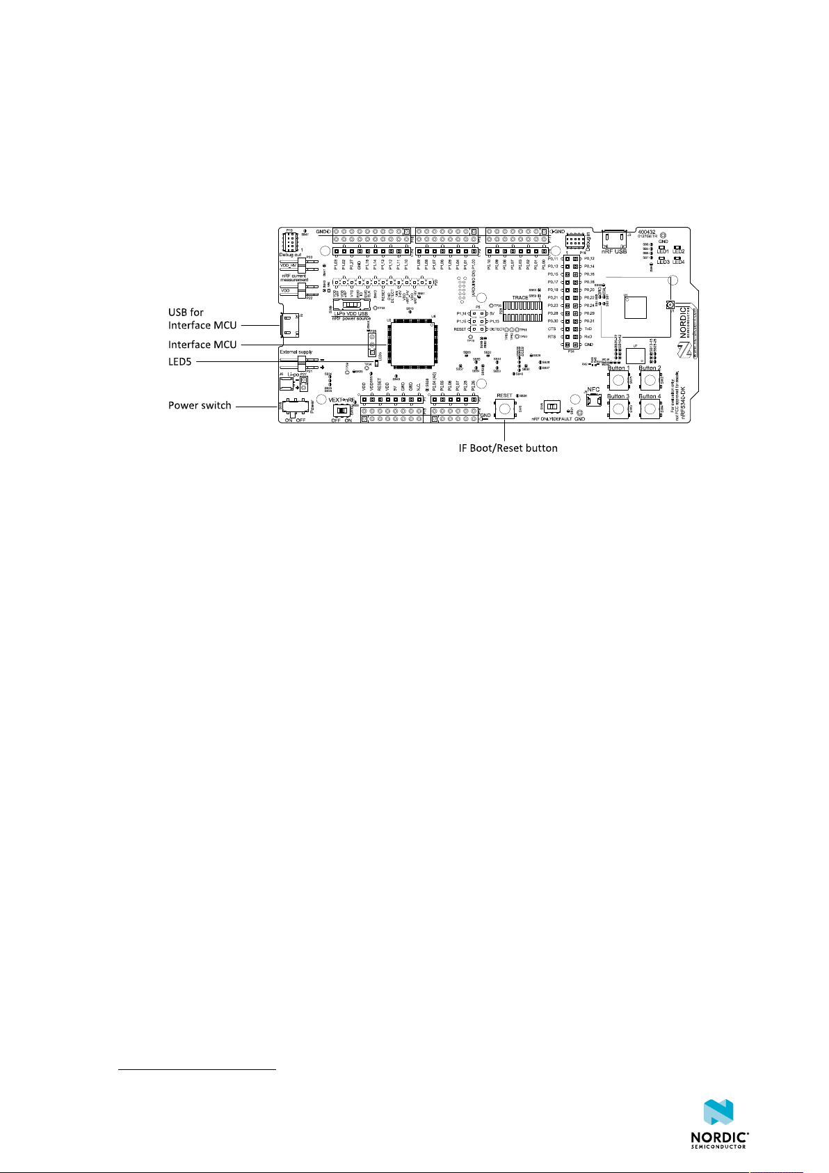
3
Interface MCU
The interface MCU on the nRF5340 DK runs SEGGER J-Link OB interface firmware and is used to program
and debug the firmware of the nRF5340 SoC.
Figure 2: Interface MCU
3.1 IF Boot/Reset button
The nRF5340 DK is equipped with an IF Boot/Reset button (SW5).
This button is connected to the interface MCU on the DK and has two functions:
• Resetting the nRF5340 SoC.
• Entering bootloader mode of the interface MCU.
The button is also used to enter the bootloader mode of the interface MCU. To enter the bootloader
mode, keep the reset button pressed while powering up the DK until LED5 starts to blink. You can power
up the DK either by disconnecting and reconnecting the USB cable or by toggling the power switch (SW8).
3.2 Virtual COM port
The onboard interface MCU features a Universal Asynchronous Receiver/Transmitter (UART) interface
through a virtual COM port.
The virtual COM port has the following features:
•
Flexible baud rate setting up to 1 Mbps.
• Dynamic Hardware Flow Control (HWFC) handling.
• Tri-stated UART lines when no terminal is connected.
The following table shows an overview of the UART connections on nRF5340 SoC and the interface MCU.
1
1
Baud rate 921 600 is not supported through the virtual COM port.
4406_638
7
Page 8

Interface MCU
GPIO nRF5340 nRF5340 UART
P0.19 RTS
P0.20 TXD
P0.21 CTS
P0.22 RXD
Table 1: Relationship of UART connections on nRF5340 and interface MCU
The UART signals are routed directly to the interface MCU. The UART pins connected to the interface MCU
are tri-stated when no terminal is connected to the virtual COM port on the computer.
Note: The terminal software used must send a Data Terminal Ready (DTR) signal to configure the
UART interface MCU pins.
The P0.19 (Request to Send (RTS)) and P0.21 (Clear to Send (CTS)) can be used freely when HWFC is
disabled on the SoC.
3.2.1 Dynamic HWFC handling
When the interface MCU receives a DTR signal from a terminal, it performs automatic HWFC detection.
Automatic HWFC detection is done by driving P0.21 (CTS) from the interface MCU and evaluating the state
of P0.19 (RTS) when the first data is sent or received. If the state of P0.19 (RTS) is high, HWFC is assumed
not to be used. If HWFC is not detected, both CTS and RTS can be used freely by the nRF application.
After a power-on reset of the interface MCU, all UART lines are tri-stated when no terminal is connected
to the virtual COM port. Due to the dynamic HWFC handling, if HWFC has been used and detected, P0.21
(CTS) will be driven by the interface MCU until a power-on reset has been performed or until a new DTR
signal is received and the detection is redone.
To ensure that the UART lines are not affected by the interface MCU, the solder bridges for these signals
can be cut and later resoldered if needed. This might be necessary if UART without HWFC is needed while
P0.19 (RTS) and P0.21 (CTS) are used for other purposes.
3.3 MSD
The interface MCU features an MSD. This makes the DK appear as an external drive on your computer.
This drive can be used for drag-and-drop programming. However, files cannot be stored on this drive. By
copying a HEX file to the drive, the interface MCU will program the file to the device.
Note:
• Windows might try to defragment the MSD part of the interface MCU. If this happens, the
interface MCU will disconnect and be unresponsive. To return to normal operation, the DK must
be power cycled.
• Your antivirus software might try to scan the MSD part of the interface MCU. Some antivirus
programs trigger a false positive alert in one of the files and quarantine the unit. If this happens,
the interface MCU will become unresponsive.
• If the computer is set up to boot from USB, it can try to boot from the DK if the DK is connected
during boot. This can be avoided by unplugging the DK before a computer restart, or changing
the boot sequence of the computer.
4406_638
8
Page 9

Interface MCU
You can also disable the MSD of the kit by using the msddisable command in J-Link Commander. To
enable, use the msdenable command. These commands take effect after a power cycle of the DK and
stay this way until changed again.
4406_638
9
Page 10

4
Hardware description
The nRF5340 DK (PCA10095) features an onboard programming and debugging solution.
In addition to radio communication, the SoC can communicate with a computer through USB and a virtual
COM port provided by the interface MCU.
4.1 Hardware drawings
nRF5340 DK hardware drawings show both sides of the PCA10095.
Figure 3: nRF5340 DK (PCA10095) front view
Figure 4: nRF5340 DK (PCA10095) back view
4.2 Block diagram
The nRF5340 DK block diagram shows the connections between the different blocks.
4406_638
10
Page 11
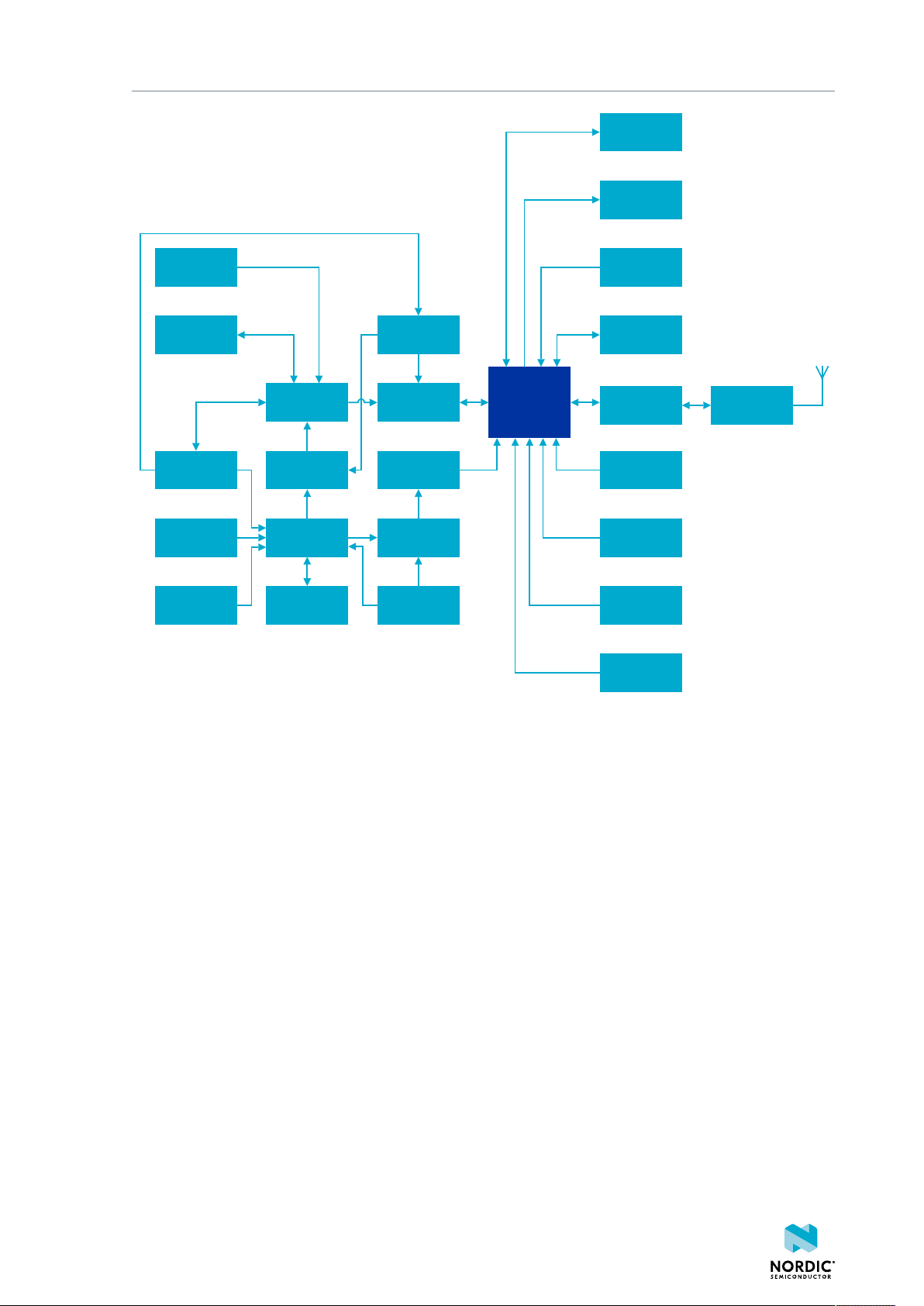
GPIO
LEDs
Hardware description
IF Boot/Reset
Debug out
Interface
MCU
IF MCU USB Analog switch
Battery
External
supply
Power supply
circuitry
Power switch
nRF only
mode switch
Analog switch
Current
measurement
nRf power
source switch
Li-ion
nRF5340
Buttons
External
memory
Matching
network
Osc
16 MHz
Osc
32.768 kHZ
Debug in
USB
RF connector
Figure 5: Block diagram
4.3 Power supply
The nRF5340 DK has multiple power options.
The power options are the following:
• USB connector J2 for the interface MCU (5 V)
• USB connector J3 for the nRF5340 SoC (5 V)
• Lithium polymer (Li-Po) battery connectors J6 or P27 (2.5–5.0 V)
• VIN 3–5 pin on P20 (3.0–5.0 V)
• External supply on P21 (1.7–3.6 V)
• Coin cell battery
4406_638
11
Page 12

Figure 6: Power supply options (front)
Hardware description
Figure 7: Power supply options (back)
4.3.1 5 V power sources
The nRF5340 DK has a 5 V boost regulator.
It gives a stable 5 V output from the following sources:
• USB connector J2 for the interface MCU
• USB connector J3 for the nRF5340 SoC
• Li-Po polymer battery connectors (J6 or P27)
• VIN 3–5 V pin on P20
Each source has a reverse protection diode to prevent current flowing in the wrong direction if multiple
sources are connected at the same time.
Figure 8: 5 V regulator and protecting diodes
4.3.2 VDD power sources
The main supply (VDD) can be sourced from the 5 V domain, external power supply, and coin cell battery.
4406_638
12
Page 13

Hardware description
For the 5 V domain, there are two regulators, one fixed 3 V buck regulator and one voltage follower
regulator that follows the VDD_nRF voltage. The coin cell battery and external power supply are not
regulated.
• 5 V domain:
• Fixed 3 V buck regulator
• VDD_nRF voltage follower
• External power supply
• Coin cell battery
For more information about power sources, see nRF5340 power source on page 15.
The power sources are routed through a set of load switches, which is controlled by logic to prioritize the
power sources in the correct manner.
If the high voltage regulator of the nRF5340 is used, the DK will be supplied from the VDD_nRF voltage
follower regardless of the state of the other power sources.
4406_638
13
Page 14
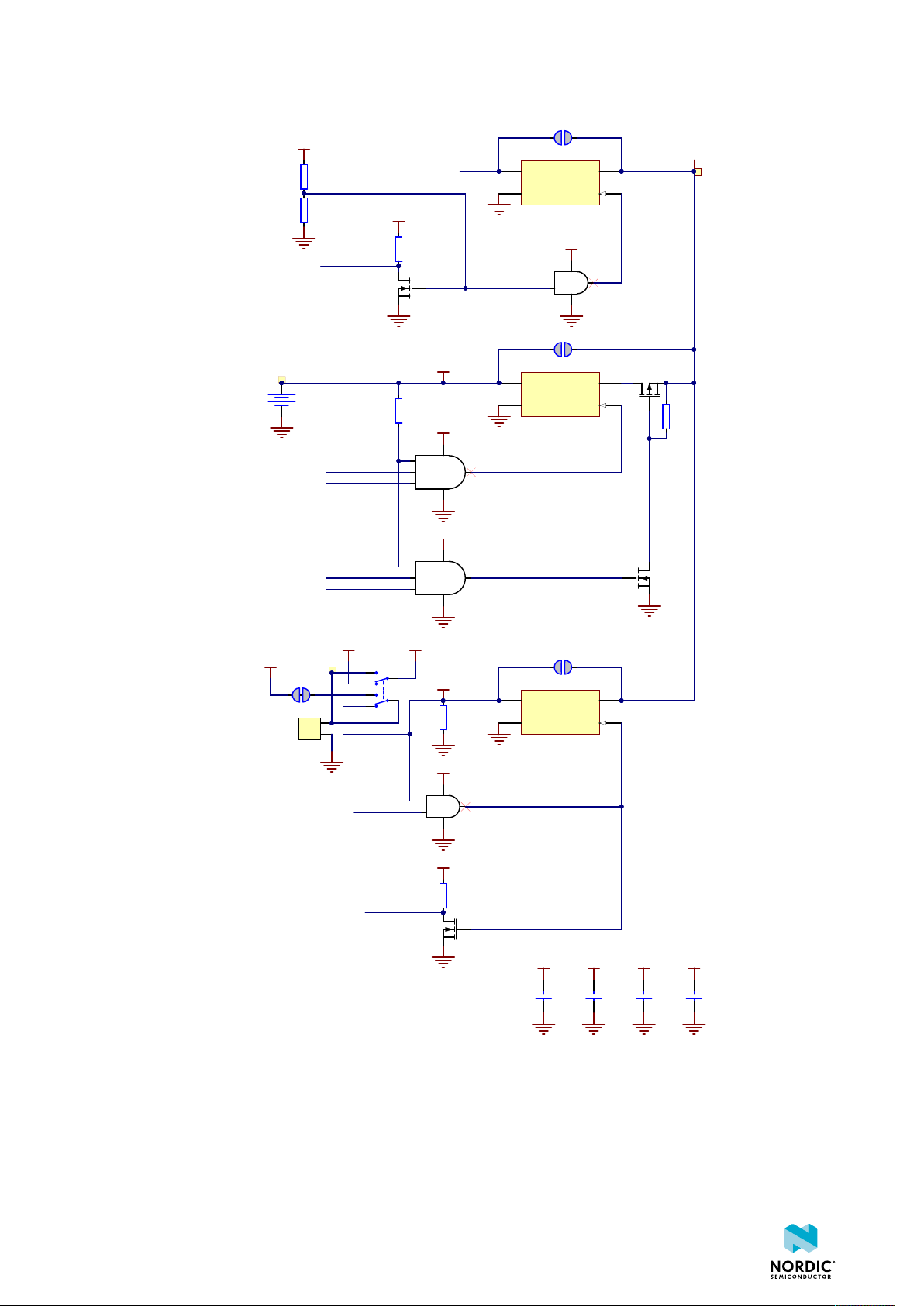
SB34
SB35
SB36
1
2
P21
Pin List 1x2, Angled
VBAT
VEXT
Q8A
TSM250N02DCQ RFG
R68
1M0
VSUPPLY
VEXT_EN
VREG_EN
VSUPPLY
VREG_EN_INV
R74
1M0
VSUPPLY
Q8B
TSM250N02DCQ RFG
VEXT_EN_INV
VREG
V5V
R65
820k
R66
470k
C68
100nF
VSUPPLY
C69
100nF
VSUPPLY
VREG_EN_INV
SW10
CAS-220TA
VDD
VSRC_NRF
GND
VCC
U24
74LVC1G08
GND
VCC
U18
74LVC1G11
GND
VCC
U16
74LVC1G08
VSUPPLY_EN
C70
100nF
VSUPPLY
R73
10M
TP27
TP26
TP29
SB58
VSUPPLY
VSUPPLY
VBAT_EN
VEXT_EN_INV
VREG_EN_INV
Q10A
PMCPB5530
Q10B
PMCPB5530
R72
1M0
R71
100k
VSUPPLY
VSUPPLY
VEXT_EN_INV
VREG_EN_INV
C71
100nF
VSUPPLY
GND
VCC
U21
74LVC1G11
+
Bat1
Bat Holder CR2032
VIN
A2
VOUT
A1
CTRL
B2
GND
B1
U13
TCK106AG
VIN
A2
VOUT
A1
CTRL
B2
GND
B1
U17
TCK106AG
VIN
A2
VOUT
A1
CTRL
B2
GND
B1
U23
TCK106AG
Hardware description
The power switches work in the way that the body diode of the internal transistor powers the VSUPPLY
net, which supplies the gates controlling the enable signal of the switches. If 5 V is present, the switches
for external supply and battery are disabled. If external supply is present, the switch for the battery is
disabled.
The power switches can be bypassed by shorting one or more solder bridges.
Figure 9: Power supply circuitry
4406_638
14
Page 15
Power source Power switch bypass Voltage level
SB37
VDD_IMCUVDD
SB48
VDD_IMCU_3VVREG
IF_OFF
IF_OFF
TP35
VINA2VOUT
A1
CTRLB2GND
B1
U19
TCK106AG
VINA2VOUT
A1
CTRLB2GND
B1
U22
TCK106AG
Regulator SB34 3.0 V
Coin cell battery SB35 Battery
External supply SB36 1.7 V–3.6 V
Table 2: Power switch bypass solder bridges
Hardware description
Figure 10: Power switch bypass solder bridges
Note: Connect only one power source at a time. Shorting the solder bridges removes the reverse
voltage protection.
4.3.3 Interface MCU power
The power for the interface MCU is routed through two load switches, one for the VDD supply and one for
the USB supply. This makes it possible to disconnect the interface MCU from the power domain when not
in use.
These switches are controlled by the presence of a USB connected to the interface MCU USB connector
(J2), and the state of the nRF only switch (SW6). See Operating modes on page 17 for more
information.
Figure 11: Interface MCU power switch
4.3.4 nRF5340 power source
The nRF5340 DK has a power source switch (SW9) for selecting between three power sources for the
nRF5340 SoC.
4406_638
15
Page 16
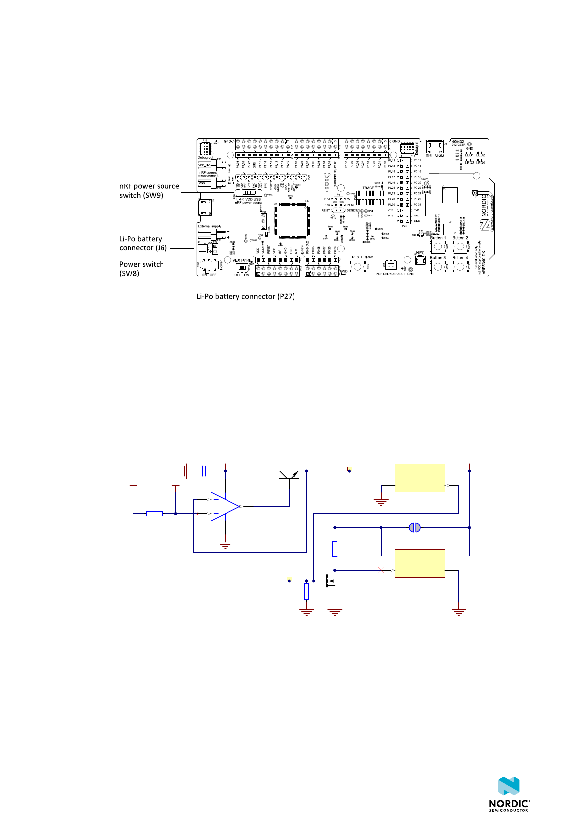
The three positions of the switch are the following:
VDD_nRF_SENSE
C65
100nF
V5V
3
2
1
A
84
V- V+
U9A
TS27L2IPT
VSENSE_SW_OUT
R70
10M
Q9
RV2C010UNT2L
R69
1M0
VDD_nRF_SENSE
VSUPPLY
Q7
FCX690BTA
SB39
VSUPPLY_EN
TP33
TP34
VIO_REF
R77
10k
VINA2VOUT
A1
CTRLB2GND
B1
U14
TCK106AG
VIN
A2
VOUT
A1
CTRL
B2
GND
B1
U12
TCK106AG
• VDD (default)
• Li-Po
• USB
Figure 12: nRF5340 DK power source switch
Hardware description
The nRF5340 SoC has a high voltage buck regulator that can support up to 5 V input. In the VDD position,
the SoC is powered either from the onboard buck regulator, coin cell battery, or external supply (P21).
In the Li-Po position, the high voltage regulator of the SoC is supplied directly from the Li-Po battery
connectors (J6 or P27). In the USB position, the USB high voltage regulator gets power from the nRF5340
USB connector (J3).
When the high voltage regulator is used, the VDD_nRF voltage can be set by the firmware of the SoC.
To make sure the rest of the DK has the same voltage level, the VDD of the DK is sourced by a regulator
following the VDD_nRF voltage when the high voltage regulator is used.
Figure 13: VDD_nRF voltage follower and switch
To make sure that the nRF5340 SoC is not powered when the nRF power switch (SW8) is OFF, two load
switches are used, one for the high voltage regulator (U15) and one for the USB supply (U20). These
switches are controlled by VDD.
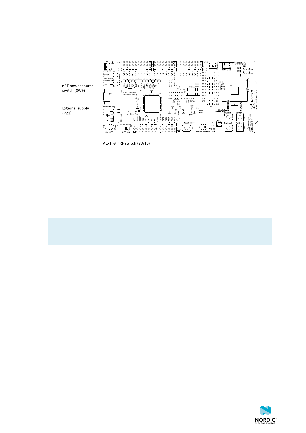
4.3.5 nRF5340 SoC direct supply
It is possible to power the SoC directly from a source without powering the rest of the DK from the same
source.
4406_638
16
Page 17
Hardware description
This is done by connecting the external source to the external supply connector (P21) and sliding the
VEXT->nRF switch (SW10) to the ON position. The nRF power source switch (SW9) must be in the VDD
position, and the allowed voltage range is 1.7–3.6 V.
Figure 14: VEXT->nRF switch (SW10)
Since it is only the nRF5340 SoC that is supplied from this source, it is recommended that the VDD domain
is supplied from a different source to prevent the pins of the SoC to be connected to unpowered devices.
To avoid voltage differences on the DK, the External supply is also connected to the input of the voltage
follower when the VEXT->nRF switch (SW10) is in the ON position. The voltage follower circuit requires 5 V
to be present on the DK, see 5 V power sources on page 12.
The voltage follower can be disconnected from the External supply by cutting SB58. To prevent leakage
due to voltage differences, the DK should be set in the nRF only mode, see nRF only mode on page 18.
Note: To reduce trace length and parasitic components, the external memory is connected to the
SoC directly instead of using analog switches. It is recommended to cut solder bridges to avoid
leakage, see External memory on page 20.
4.4 Operating modes
The nRF5340 DK has various modes of operation.
4.4.1 USB detect
To detect when USB for the interface MCU is connected, there is a circuit sensing the VBUS of USB
connector J2.
When the USB cable is connected, the VDD is propagated to the USB_DETECT signal.
4406_638
17
Page 18
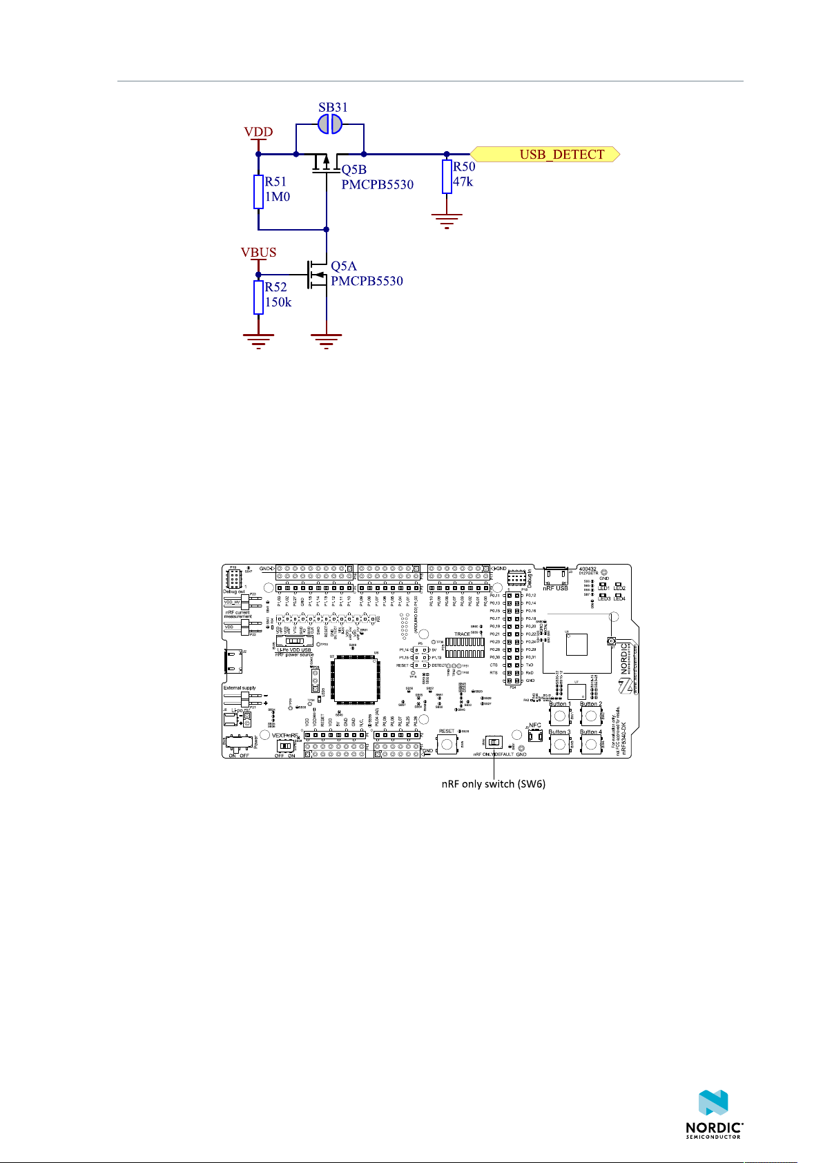
Hardware description
Figure 15: USB detect
4.4.2 nRF only mode
The nRF only mode disconnects the power supply, external memory, and LEDs of the interface MCU. It also
disconnects the signal lines between the nRF5340 SoC and the interface MCU using analog switches.
This is done to isolate the chip on the DK as much as possible, and can be of use when measuring currents
on low-power applications.
The power supply of the external memory can be changed to maintain operation in the nRF only mode.
See External memory on page 20.
Figure 16: nRF ONLY switch (SW6)
4.4.3 Signal switches
On the nRF5340 DK, there are multiple analog switches that are used to connect and disconnect signals
based on different scenarios.
4406_638
18
Page 19
Hardware description
TP3
TP2
TP4
TP1
TP5
TP6
TP7
SB54
SB55
SB51
SB53
SB50
SB52
SB57
SB56
NC1
1
IN 1-2
2
NO2
3
COM2
4
NC2
5
GND
6
NO3
7
COM3
8
NC3
9
IN 3-4
10
NO4
11
COM4
12
NC4
13
VCC
14
NO1
15
COM1
16
U5
FSA2466UMX
C42
100nF
VDD
NC1
1
IN 1-2
2
NO2
3
COM2
4
NC2
5
GND
6
NO3
7
COM3
8
NC3
9
IN 3-4
10
NO4
11
COM4
12
NC4
13
VCC
14
NO1
15
COM1
16
U3
FSA2466UMX
NC1
1
IN 1-2
2
NO2
3
COM2
4
NC2
5
GND
6
NO3
7
COM3
8
NC3
9
IN 3-4
10
NO4
11
COM4
12
NC4
13
VCC
14
NO1
15
COM1
16
U6
FSA2466UMX
C41
100nF
C45
100nF
IF_OFF
IF_OFF
IF_OFF
VDD
VDD
TP8
IMCU_BOOT
USB_DETECT
IF_OFF
VDD
SB46
RESET_PIN
SB45
IMCU_BOOT
SB42
SB43
RESET_PIN
SB44
nRF_ONLY
BOOT/RESET
IF_OFF
R48 4k7
R49 4k7
SHIELD_DETECT
VDD
VDD
IF_OFF
R44
10k
SW6
CAS-220TA
RESET
RESET
RESET
SWDCLK
SWDIO
P0.11/TRACEDATA0
SWD3_RESET
SWD3_SWDCLK
SWD3_SWDIO
SWD3_SWO
VCOM2_CTS
VCOM2_RTS
VCOM2_RxD
VCOM2_TxD
P1.03
P1.02
UART_1_CTS
UART_1_RTS
UART_1_RxD
UART_1_TxD
TP54
TP57
TP56
TP55
SB28
SB30
SB27
SB29
NC1
1
IN 1-2
2
NO2
3
COM2
4
NC2
5
GND
6
NO3
7
COM3
8
NC3
9
IN 3-4
10
NO4
11
COM4
12
NC4
13
VCC
14
NO1
15
COM1
16
U25
FSA2466UMX
C24
100nF
VDD
IF_OFF
IF_OFF
UART_2_CTS
UART_2_RTS
UART_2_RxD
UART_2_TxD
VCOM0_CTS
VCOM0_RTS
VCOM0_RxD
VCOM0_TxD
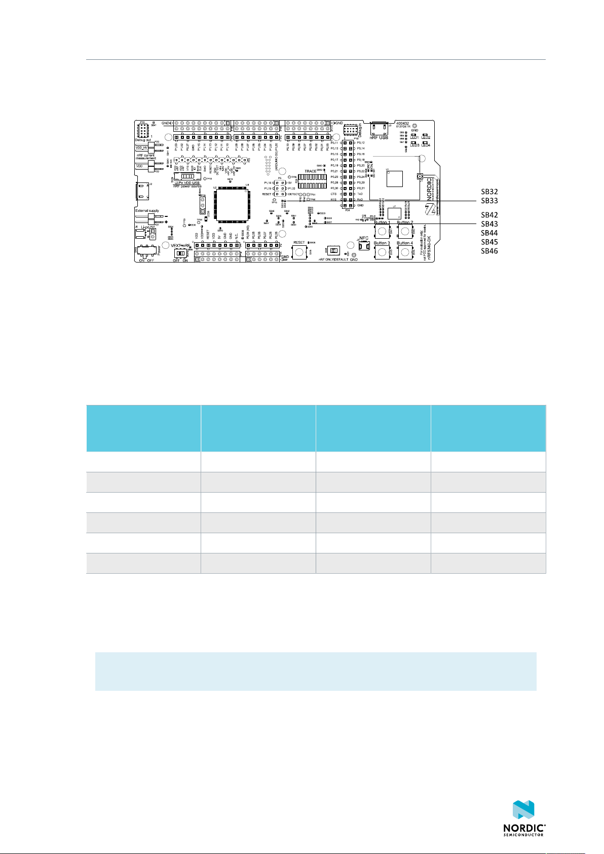
The USB and SW6 control the signal switches by using USB_DETECT as an input to SW6. Therefore, the
interface MCU can be disconnected either by unplugging the USB cable from J2 or by toggling the nRF
ONLY switch SW6.
The signal controls a set of switches (U3, U5, U6) that break the connection between the nRF5340 and the
interface MCU, and control the power for the interface MCU. For more information, see Interface MCU
power on page 15.
Switches U3 and U5 break the connection of the UART lines and SWD/RESET lines. In addition, the
signal controls the routing of the RESET signal depending on user preference when the interface MCU is
connected/disconnected.
• When the interface MCU is connected, shorting SB46 will connect the RESET pin in the Arduino
interface to the BOOT input of the interface MCU.
• Shorting SB43 will connect the RESET pin in the Arduino interface to the IF Boot/Reset button.
4406_638
Figure 17: Signal switches
19
Page 20
Hardware description
When a shield is connected, there are two analog switches connecting the pull-up resistors to the I2C bus
lines (SDA and SCL). This function is using one ground pin on the Arduino shield to control the switch. This
feature can be disabled by cutting SB33. To permanently enable pull-up resistors, short SB32.
Figure 18: Solder bridges: Shield detect and reset behavior
4.5 External memory
The nRF5340 DK has a 64 Mb external flash memory. The memory is a multi-I/O memory supporting both
regular SPI and Quad SPI.
The memory is connected to the chip using the following GPIOs:
GPIO Flash memory pin Solder bridge for
memory use (default:
shorted)
P0.18 CS SB13 SB23
P0.17 SCLK SB11 SB21
P0.13 SIO_0/SI SB12 SB22
P0.14 SIO_1/SO SB14 SB24
P0.15 SIO_2/WP SB15 SB25
P0.16 SIO_3/HOLD SB10 SB20
Table 3: Flash memory GPIO usage and connecting solder bridges
To use the GPIOs for a purpose other than the onboard external memory and have them available on the
P24 connector, six solder bridges (SB10–SB15) must be cut and six solder bridges (SB20–SB25) must be
shorted. See the following figure for details.
Solder bridge for GPIO
use (default: open)
Note: If debugging the QSPI communication is needed, the SB20–SB25 can be shorted without
cutting SB10–SB15, but the pins should not be driven externally.
4406_638
20
Page 21

Hardware description
Figure 19: Configuring GPIOs for external memory
By default, the power supply of the external memory is coming from the VDD domain and it is controlled
by the nRF only switch (SW6). In the nRF only mode, there are two optional power sources for keeping
the external memory powered, VDD and VDD_nRF. If VDD_nRF is selected, the power consumption of the
external memory will be added to the nRF5340 current measured on P22 or P23. See the following table
for configuration:
Power source Solder bridge Default state
VDD_PER SB16 Shorted
VDD SB17 Open
VDD_nRF SB18 Open
Table 4: Flash memory power source configuration
4.6 Connector interface
Access to the nRF5340 GPIOs is available from connectors P2, P3, P4, P5, P6, and P24.
The P1 connector provides access to ground and power on the nRF5340 DK.
4406_638
21
Page 22

Hardware description
Figure 20: nRF5340 DK connectors
Some of the signals are also available on connectors P7, P8, P9, P10, P11, and P12, which are on the
bottom side of the DK. By mounting pin lists on the connector footprints, the nRF5340 DK can be used as a
shield for Arduino motherboards2 or other boards that follow the Arduino standard.
For easy access to GPIO, power, and ground, the signals can also be found on the through-hole connectors
P13–P17.
Note:
Some pins have default settings:
• P0.00 and P0.01 are used for the 32.768 kHz crystal and are not available on the connectors. For
more information, see 32.768 kHz crystal on page 24.
• P0.19, P0.20, P0.21, and P0.22 are used by the UART connected to the interface MCU. For more
information, see Virtual COM port on page 7.
• P0.02 and P0.03 are by default used by NFC1 and NFC2. For more information, see NFC antenna
interface on page 27.
• P0.08–P0.09 and P0.23–P0.24 are by default connected to the buttons and P0.28–P0.31 are
connected to the LEDs. For more information, see Buttons and LEDs on page 23.
• P0.13–P0.18 are by default connected to the external memory. For more information, see
External memory on page 20.
When the nRF5340 DK is used as a shield together with an Arduino standard motherboard, the Arduino
signals are routed as shown in the following figure.
2
Only 3.3 V Arduino boards.
4406_638
22
Page 23

Hardware description
Figure 21: Arduino signals routing on the nRF5340 DK
4.6.1 Mapping of analog pins
The table shows the mapping between GPIO pins, analog inputs, and the corresponding Arduino analog
input naming.
GPIO Analog input Arduino naming
P0.04 AIN0 A0
P0.05 AIN1 A1
P0.06 AIN2 A2
P0.07 AIN3 A3
P0.25 AIN4 A4
P0.26 AIN5 A5
Table 5: Mapping of analog pins
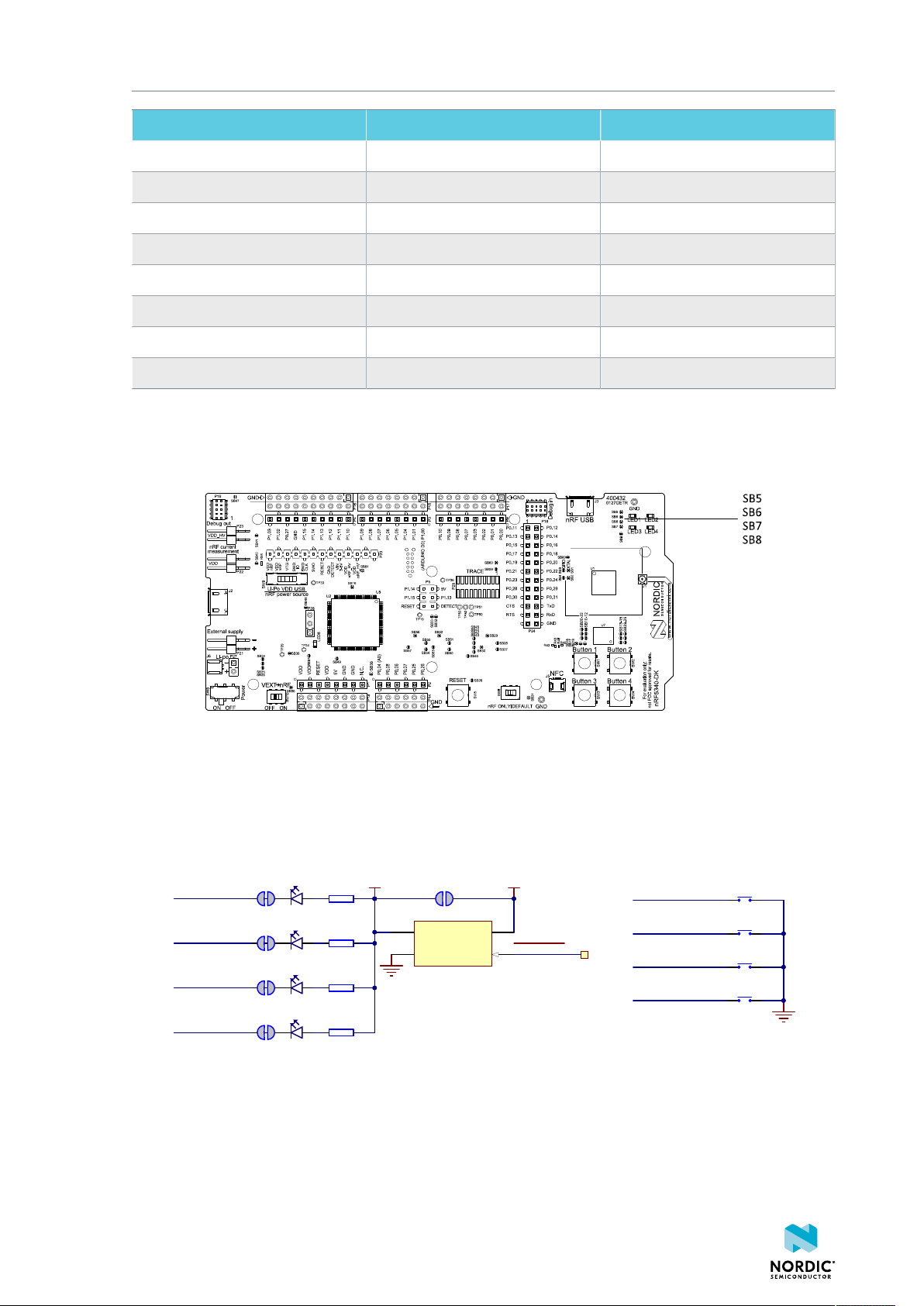
4.7 Buttons and LEDs
The four buttons and four LEDs on the nRF5340 DK are connected to dedicated GPIOs on the nRF5340 SoC.
4406_638
23
Page 24
Hardware description
R3
220R
R2
220R
SB6
VDD_PER
R4
220R
SB7
R5
220R
SB8
SB5
LED1
L0603G
LED2
L0603G
LED3
L0603G
LED4
L0603G
SB9
VDD
nRF_ONLY
TP22
P0.28/AIN7
P0.30
P0.31
P0.29
VIN
A2
VOUT
A1
CTRL
B2
GND
B1
U4
TCK106AG
SW1
PB SW
SW2
PB SW
SW3
PB SW
SW4
PB SW
P0.23
P0.24
P0.08/TRACEDATA3
P0.09/TRACEDATA2
Part GPIO Solder bridge
Button 1 P0.23 -
Button 2 P0.24 -
Button 3 P0.08 -
Button 4 P0.09 -
LED 1 P0.28 SB5
LED 2 P0.29 SB6
LED 3 P0.30 SB7
LED 4 P0.31 SB8
Table 6: Button and LED connection
If P0.28–P0.31 are needed elsewhere, the LEDs can be disconnected by cutting the short on SB5–SB8. See
Figure 22: Disconnecting the LEDs on page 24 for more information.
Figure 22: Disconnecting the LEDs
The buttons are active low, meaning that the input will be connected to ground when the button is
activated. The buttons have no external pull-up resistor, and therefore, to use the buttons, the P0.08,
P0.09, P0.23, P0.24 pins must be configured as input with an internal pull-up resistor.
The LEDs are active low, meaning that writing a logical zero (0) to the output pin will illuminate the LED.
Figure 23: Button and LED configuration
4.8 32.768 kHz crystal
The nRF5340 SoC can use an optional 32.768 kHz crystal (X2) for higher accuracy and lower average power
consumption.
4406_638
24
Page 25

Hardware description
On the nRF5340 DK, P0.00 and P0.01 are used for the 32.768 kHz crystal by default and are not available
as GPIO on the connectors.
Note: When using ANT/ANT+™, the 32.768 kHz crystal (X2) is required for correct operation.
If P0.00 and P0.01 are needed as normal I/Os, the 32.768 kHz crystal can be disconnected and the
GPIO routed to the connectors. Cut the shorting track on SB1 and SB2, and solder SB3 and SB4. See the
following figure for reference.
Figure 24: Configuring P0.00 and P0.01
Figure 25: 32.768 kHz crystal and SB1–SB4
4.9 Debug input and trace
The Debug in connector (P18) makes it possible to connect external debuggers for debugging when the
interface MCU USB cable is not connected or the DK is in nRF only mode.
Figure 26: Debug input and trace connectors
For trace, a footprint for a 20-pin connector is available (P25). If trace functionality is required, it is
possible to mount a 2×10 pin 1.27 mm pitch surface-mount pin header.
4406_638
25
Page 26
Hardware description
GPIO Trace Default use
P0.12 TRACECLK
P0.11 TRACEDATA[0]
P0.10 TRACEDATA[1]
P0.09 TRACEDATA[2] Button 4
P0.08 TRACEDATA[3] Button 3
Table 7: Default and Trace GPIOs
The reference voltage for the debug input and trace is by default connected to VDD_nRF'. This can be
connected to the VDD by cutting SB60 and soldering SB59.
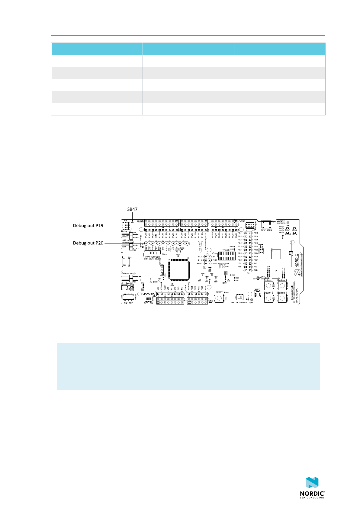
4.10 Debug output
The nRF5340 DK supports programming and debugging external boards with nRF51 Series , nRF52 Series,
or nRF53 Series SoCs. To debug an external board with SEGGER J-Link OB IF, connect to the Debug out
connector (P19) with a 10-pin cable.
Figure 27: Debug output connector
When the external board is powered, the interface MCU will detect the supply voltage of the board and
program/debug the target chip on the external board instead of the onboard nRF5340 SoC.
Note: The voltage supported by external debugging/programming is VDD voltage. Normally, this
is 3 V when running from USB, but if the onboard nRF5340 SoC is supplied from either USB or LiIon, the nRF power source switch (SW9) is in either Li-Po or USB position, and VDD can be set by
the nRF5340 firmware. Make sure the voltage level of the external board matches the VDD of the
nRF5340 DK.
You can also use P20 as a debug out connection to program shield-mounted targets. For both P19 and
P20, the interface MCU will detect the supply voltage on the mounted shield and program/debug the
target.
If the interface MCU detects target power on both P19 and P20, it will by default program/debug the
target connected to P19.
If it is inconvenient to have a separate power supply on the external board, the nRF5340 DK can supply
power through the Debug out connector (P19). To enable this, short solder bridge SB47. While SB47 is
shorted, it is not possible to program the onboard nRF5340 SoC even if the external board is unplugged.
4406_638
26
Page 27
Hardware description
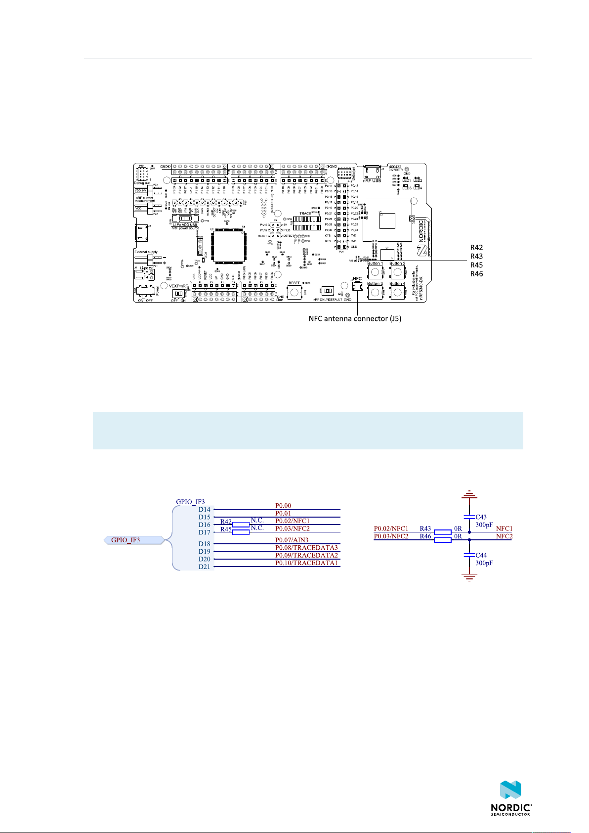
4.11 NFC antenna interface
The nRF5340 DK supports an NFC tag.
NFC-A listen mode operation is supported on the nRF5340 SoC. The NFC antenna input is available on
connector J5 on the nRF5340 DK.
Figure 28: NFC antenna connector
NFC uses two pins, W1 (NFC1) and AA1 (NFC2), to connect the antenna. These pins are shared with GPIOs
(P0.02 and P0.03) and the PROTECT field in the NFCPINS register in UICR defines the usage of these pins
and their protection level against abnormal voltages. The content of the NFCPINS register is reloaded at
every reset.
Note: The NFC pins are enabled by default. NFC can be disabled and GPIOs enabled by setting the
CONFIG_NFCT_PINS_AS_GPIOS to y. See Configuring your application for instructions.
Pins W1 and AA1 are by default configured to use the NFC antenna, but if they are needed as normal
GPIOs, R43 and R46 must be NC and R42 and R45 must be shorted by 0R.
Figure 29: NFC input
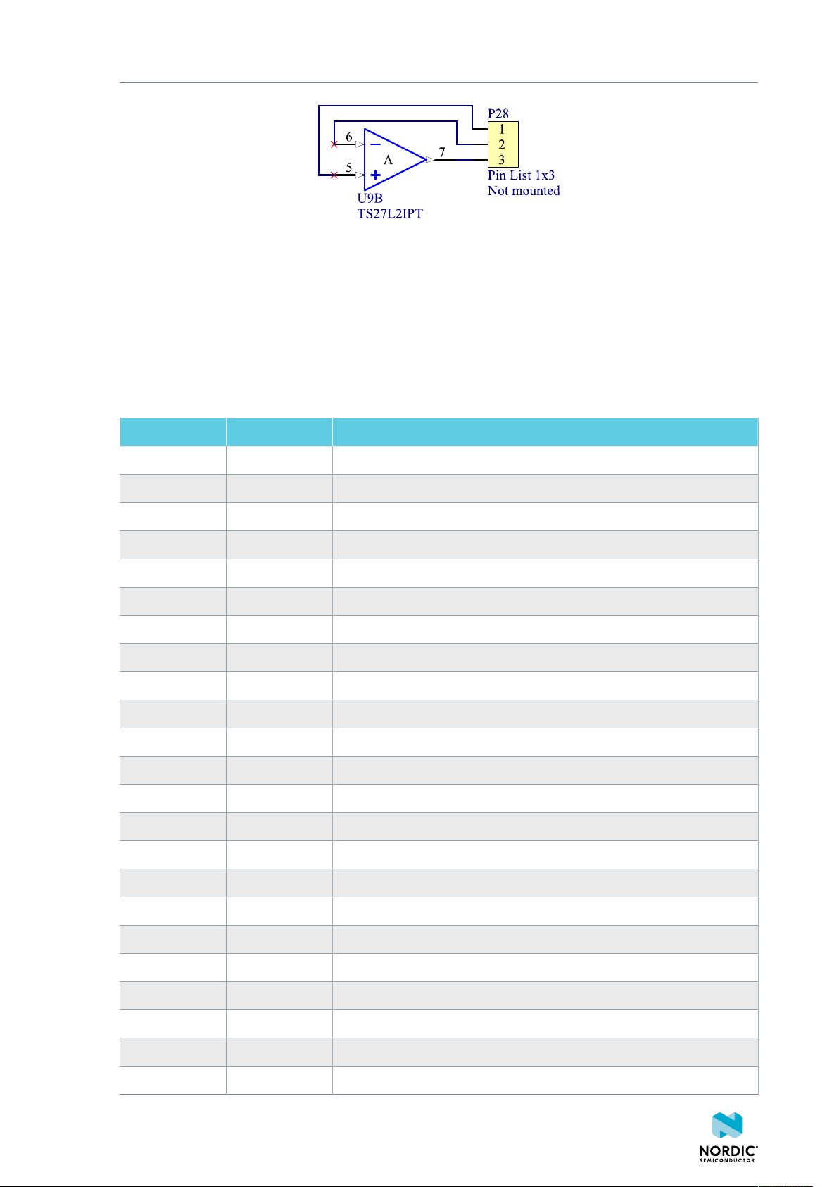
4.12 Extra op-amp
The voltage follower for the power supply uses a dual package op-amp.
The extra op-amp has been routed out to a connector (P28, not mounted) so that it is accessible for the
user.
For more information on the power supply, see Power supply on page 11.
4406_638
27
Page 28
Hardware description
Figure 30: Extra op-amp
4.13 Solder bridge configuration
The nRF5340 DK has a range of solder bridges for enabling or disabling functionality on the DK. Changes to
these are not needed for normal use of the DK.
The following table is a complete overview of the solder bridges on the nRF5340 DK.
Solderbridge Default Function
SB1 Closed Cut to disconnect the 32.768 kHz on P0.01
SB2 Closed Cut to disconnect the 32.768 kHz on P0.00
SB3 Open Short to enable P0.01 as normal GPIO
SB4 Open Short to enable P0.00 as normal GPIO
SB5 Closed Cut to disconnect LED1
SB6 Closed Cut to disconnect LED2
SB7 Closed Cut to disconnect LED3
SB8 Closed Cut to disconnect LED4
SB9 Open Short to bypass peripheral power switch
SB10 Closed Cut to disconnect the QSPI memory from P0.16
SB11 Closed Cut to disconnect the QSPI memory from P0.17
SB12 Closed Cut to disconnect the QSPI memory from P0.13
SB13 Closed Cut to disconnect the QSPI memory from P0.18
SB14 Closed Cut to disconnect the QSPI memory from P0.14
SB15 Closed Cut to disconnect the QSPI memory from P0.15
SB16 Closed Cut to disconnect QSPI memory power supply from VDD_PER
SB17 Open Short to connect QSPI memory power supply to VDD
SB18 Open Short to connect QSPI memory power supply to VDD_nRF
SB20 Open Short to enable P0.16 as a normal GPIO
SB21 Open Short to enable P0.17 as a normal GPIO
SB22 Open Short to enable P0.13 as a normal GPIO
SB23 Open Short to enable P0.18 as a normal GPIO
SB24 Open Short to enable P0.14 as a normal GPIO
4406_638
28
Page 29
Hardware description
Solderbridge Default Function
SB25 Open Short to enable P0.15 as a normal GPIO
SB26 Closed Cut to disable the rgw pull-up resistor of the BOOT/RESET line
SB31 Open Short to bypass the USB detect switch
SB32 Open Short to permanently enable the I2C pull-up resistors
SB33 Closed Cut to permanently disable the I2C pull-up resistors
SB34 Open Short to bypass the power switch on the USB power
SB35 Open Short to bypass the power switch on the coin cell battery power
SB36 Open Short to bypass the power switch on the external supply power
SB37 Open Short to bypass the interface MCU power switch
SB38 Closed Cut to disable VDD power to the Arduino interface
SB39 Open Short to bypass the power switch for regulator, coin cell, or external
supply
SB40 Closed Cut for current measurements of the VDD_nRF
SB41 Closed Cut for current measurements of the VDD_nRF_HV
SB42 Closed Cut to disconnect IF Boot/Reset button from nRF5340 reset pin when
the interface MCU is disconnected
SB43 Open Short to connect IF Boot/Reset button to RESET pin on the Arduino
interface
SB44 Open Short to connect the RESET pin on the Arduino interface to the
nRF5340 reset pin
SB45 Open Short to connect the RESET pin on the Arduino interface to the
interface nRF5340 reset pin when the interface MCU is disconnected
SB46 Open Short to connect the RESET pin on the Arduino interface to the
interface MCU Boot when the interface MCU is disconnected
SB47 Open Short to enable power supply of the external device when using the
debug out connector
SB48 Open Short to bypass the interface MCU USB power switch
SB50 Closed Cut to disconnect the nRF5340 CTS line from the signal switch and
interface MCU
SB51 Closed Cut to disconnect the nRF5340 RTS line from the signal switch and
interface MCU
SB52 Closed Cut to disconnect the nRF5340 RxD line from the signal switch and
the interface MCU
SB53 Closed Cut to disconnect the nRF5340 TxD line from the signal switch and
interface MCU
SB54 Closed Cut to disconnect the nRF5340 SWDIO line from the signal switch and
interface MCU
SB55 Closed Cut to disconnect the nRF5340 SWDCLK line from the signal switch
and interface MCU
4406_638
29
Page 30

Hardware description
Solderbridge Default Function
SB56 Closed Cut to disconnect the nRF5340 RESET line from the signal switch and
interface MCU
SB57 Closed Cut to disconnect the nRF5340 SWO line from the signal switch and
the interface MCU
SB58 Closed Cut to disconnect voltage follower from external supply when SW10
is in ON position
SB59 Open Solder to connect debug in and trace reference voltage to VDD
SB60 Closed Cut to disconnect debug in and trace reference voltage from
VDD_nRF'
SB80 Open Short to bypass the power switch for the VBUS of nRF5340
SB81 Open Short to bypass the power switch for VDD_HV of nRF5340
Table 8: Solder bridge configuration
4406_638
30
Page 31
5
Measuring current
The current drawn by the nRF5340 SoC can be monitored on the nRF5340 DK.
Current can be measured using various test instruments. Examples of test equipment are the following:
• Power analyzer
• Oscilloscope
• Ampere meter
• Power Profiler Kit
Power analyzer and Power Profiler Kit measurements are not described in this document. For more
information on Power Profiler Kit, see Power Profiler Kit User Guide.
For measuring instructions, see Using an oscilloscope for current profile measurement on page 32 and
Using an ampere meter for current measurement on page 33.
The nRF5340 SoC has two possible power supplies, VDD (1.7–3.6 V) and VDDH (2.5–5.5 V). The nRF5340
DK is prepared for measuring current on both domains. Only the VDD domain current measurement
is described here, but the approach is the same with the VDDH supply. See the following table for the
corresponding components.
Component VDD VDDH
Measurement connector P22 P23
Solder bridge SB40 SB41
Series resistor R64 R67
Table 9: Components for current measurement on VDD and VDDH
Note: When measuring the current consumption:
• It is not recommended to use a USB connector to power the DK during current measurements
due to potential noise from the USB power supply. However, when measuring current on
an application using the USB interface of the nRF5340 SoC, the USB must be connected. It is
recommended to power the DK from a coin cell battery, external power supply on connector
P21 (1.7–3.6 V), or through the Li-Po connector J6 or P27 (2.5–5.0 V).
• The current measurements will become unreliable when a serial terminal is connected to the
virtual COM port.
• After programming the nRF5340 SoC, the USB for the interface MCU must be disconnected.
For more information on current measurement, see the tutorial Current measurement guide:
Introduction.
5.1 Preparing the DK
To measure current, you must first prepare the DK.
The suggested configurations actually split the power domains for the nRF5340 SoC and the rest of the DK.
4406_638
31
Page 32
Measuring current
Figure 31: Preparing the DK for current measurements
• To put P22 in series with the load, cut the PCB track shorting solder bridge SB40.
• To restore normal kit function after measurement, solder SB40 or apply a jumper on P22.
• To reprogram the nRF5340 SoC while the DK is prepared for current measurements, remove
measurement devices from P22, and then connect the USB cable.
5.2 Using an oscilloscope for current profile measurement
An oscilloscope can be used to measure both the average current over a given time interval and capture
the current profile.
Make sure you have prepared the DK as described in section Preparing the DK on page 31.
1. Mount a 10 Ω resistor on the footprint for R64.
2. Connect an oscilloscope in differential mode or similar with two probes on the pins of the P22
connector as shown in the following figure.
3. Calculate or plot the instantaneous current from the voltage drop across the 10 Ω resistor by taking the
difference of the voltages measured on the two probes. The voltage drop will be proportional to the
current. The 10 Ω resistor will cause a 10 mV drop for each 1 mA drawn by the circuit being measured.
The plotted voltage drop can be used to calculate the current at a given point in time. The current can
then be averaged or integrated to analyze current and energy consumption over a period.
4406_638
Figure 32: Current measurement with an oscilloscope
32
Page 33

Measuring current
Some tips to reduce noise:
• Use probes with 1× attenuation
• Enable averaging mode to reduce random noise
• Enable high resolution function if available
Use a minimum of 200 kSa/s (one sample every 5 µs) to get the correct average current measurement.
5.3 Using an ampere meter for current measurement
The average current drawn by the nRF5340 SoC can be measured using an ampere meter. This method
monitors the current in series with the nRF device.
Make sure you have prepared the DK as described in section Preparing the DK on page 31.
Connect an ampere meter between the pins of connector P22 as shown in the following figure.
Figure 33: Current measurement with an ampere meter
Note: An ampere meter will measure the average current drawn by the nRF5340 SoC if:
• The SoC is in a state where it draws a constant current, or, the activity on the device changing
load current, like BLE connection events, is repeated continuously and has a short cycle time
(less than 100 ms) so that the ampere meter will average whole load cycles and not parts of the
cycle.
• The dynamic range of the ampere meter is wide enough to give accurate measurements from 1
µA to 15 mA.
We recommend that you use a true RMS ampere meter.
4406_638
33
Page 34
6
RF measurements
The nRF5340 DK is equipped with a small coaxial connector (J1) for conducting measurements of the RF
signal using a spectrum analyzer.
The connector is of SWF type (Murata part no. MM8130-2600) with an internal switch. By default, when
no cable is attached, the RF signal is routed to the onboard trace antenna.
A test probe is available (Murata part no. MXHS83QE3000) with a standard SMA connection on the other
end for connecting instruments (the test probe is not included with the kit). When connecting the test
probe, the internal switch in the SWF connector will disconnect the onboard antenna and connect the RF
signal from the nRF5340 SoC to the test probe.
Figure 34: Connecting a spectrum analyzer
The connector and test probe will add loss to the RF signal, which should be taken into account when
measuring. See the following table for more information.
Frequency (MHz) Loss (dB)
2440 1.0
4880 1.7
7320 2.6
Table 10: Typical loss in connector and test probe
4406_638
34
Page 35

Glossary
Clear to Send (CTS)
In flow control, the receiving end is ready and telling the far end to start sending.
Data Terminal Ready (DTR)
A control signal in RS-232 serial communications transmitted from data terminal equipment, such as
a computer, to data communications equipment.
Development Kit (DK)
A development platform used for application development.
Hardware Flow Control (HWFC)
A handshaking mechanism used to prevent an overflow of bytes in modems. It is utilizing two
dedicated pins on the RS-232 connector, Request to Send and Clear to Send.
Integrated Development Environment (IDE)
A software application that provides facilities for software development.
Mass Storage Device (MSD)
Any storage device that makes it possible to store and port large amounts of data in a permanent
and machine-readable fashion.
Near Field Communication (NFC)
A standards-based short-range wireless connectivity technology that enables two electronic devices
to establish communication by bringing them close to each other.
NFC-A Listen Mode
Initial mode of an NFC Forum Device when it does not generate a carrier. The device listens for the
remote field of another device. See Near Field Communication (NFC) on page 35.
Operational Amplifier (op-amp)
A high-gain voltage amplifier that has a differential input and, usually, a single output.
Receive Data (RXD)
A signal line in a serial interface that receives data from another device.
Request to Send (RTS)
In flow control, the transmitting end is ready and requesting the far end for a permission to transfer
data.
Root Mean Square (RMS)
An RMS meter calculates the equivalent direct current (DC) value of an alternating current (AC)
waveform. A true-RMS meter can accurately measure both pure waves and the more complex
nonsinusoidal waves.
SubMiniature Version A (SMA) Connector
A semi-precision coaxial RF connector for coaxial cables with a screw-type coupling mechanism.
4406_638
35
Page 36

System on Chip (SoC)
A microchip that integrates all the necessary electronic circuits and components of a computer or
other electronic systems on a single integrated circuit.
Transmit Data (TXD)
A signal line in a serial interface that transmits data to another device.
Universal Asynchronous Receiver/Transmitter (UART)
A hardware device for asynchronous serial communication between devices.
4406_638
36
Page 37

Acronyms and abbreviations
These acronyms and abbreviations are used in this document.
CTS
Clear to Send
DK
Development Kit
DTR
Data Terminal Ready
HWFC
Hardware Flow Control
IDE
Integrated Development Environment
MSD
Mass Storage Device
NFC
Near Field Communication
op-amp
Operational Amplifier
RMS
Root Mean Square
RTS
Request to Send
RXD
Receive Data
SMA
SubMiniature version A
SoC
System on Chip
TXD
Transmit Data
UART
Universal Asynchronous Receiver/Transmitter
4406_638
37
Page 38

Recommended reading
In addition to the information in this document, you may need to consult other documents.
Nordic documentation
• nRF5340 Product Specification
• nRF5340 Compatibility Matrix
• nRF5340 Errata
• nRF Connect SDK
4406_638
38
Page 39

FCC regulatory notice
The following regulatory notices apply to the nRF5340 DK.
This kit has not been authorized under the rules of the FCC and is designed to allow:
• Product developers to evaluate electronic components, circuitry, or software associated with the kit to
determine whether to incorporate such items in a finished product.
• Software developers to write software applications for use with the end product.
This kit is not a finished product and when assembled may not be resold or otherwise marketed unless all
required FCC equipment authorizations are first obtained. Operation is subject to the condition that this
product not cause harmful interference to licensed radio stations and that this product accept harmful
interference. Unless the assembled kit is designed to operate under part 15, part 18 or part 95 of 47 CFR
Chapter I - FCC, the operator of the kit must operate under the authority of an FCC license holder or must
secure an experimental authorization under part 5 of the latter chapter.
4406_638
39
Page 40

Legal notices
By using this documentation you agree to our terms and conditions of use. Nordic Semiconductor may
change these terms and conditions at any time without notice.
Liability disclaimer
Nordic Semiconductor ASA reserves the right to make changes without further notice to the product to
improve reliability, function, or design. Nordic Semiconductor ASA does not assume any liability arising out
of the application or use of any product or circuits described herein.
Nordic Semiconductor ASA does not give any representations or warranties, expressed or implied, as to
the accuracy or completeness of such information and shall have no liability for the consequences of use
of such information. If there are any discrepancies, ambiguities or conflicts in Nordic Semiconductor’s
documentation, the Product Specification prevails.
Nordic Semiconductor ASA reserves the right to make corrections, enhancements, and other changes to
this document without notice.
Life support applications
Nordic Semiconductor products are not designed for use in life support appliances, devices, or systems
where malfunction of these products can reasonably be expected to result in personal injury.
Nordic Semiconductor ASA customers using or selling these products for use in such applications do so
at their own risk and agree to fully indemnify Nordic Semiconductor ASA for any damages resulting from
such improper use or sale.
RoHS and REACH statement
Complete hazardous substance reports, material composition reports and latest version of Nordic's REACH
statement can be found on our website www.nordicsemi.com.
Trademarks
All trademarks, service marks, trade names, product names, and logos appearing in this documentation
are the property of their respective owners.
Copyright notice
©
2020 Nordic Semiconductor ASA. All rights are reserved. Reproduction in whole or in part is prohibited
without the prior written permission of the copyright holder.
4406_638
40
 Loading...