

Datasheet NMAQ31750FS, NMAR31750AE, NMAR31750FB, NMAR31750FE, NMAR31750FD Datasheet (DYNEX)
...Page 1
MA31750
1/42
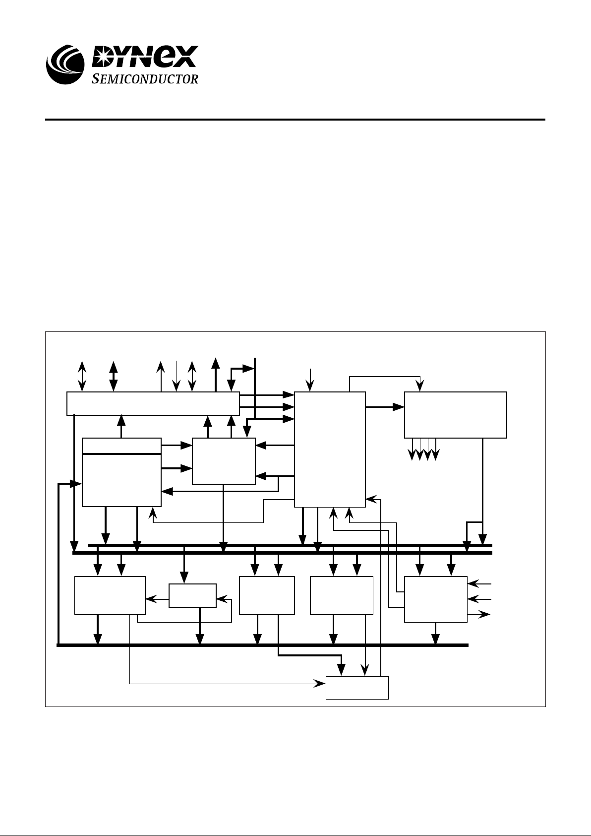
The Dynex Semiconductor MA31750 is a single-chip
microprocessor that implements the full MIL-STD-1750A
instruction set architecture, or Option 2 of Draft MIL-STD1750B. The processor executes all mandatory instructions and
many optional features are also included. Interrupts, fault
handling, memory expansion, Console, timers A and B, and
their related optional instructions are also supported in full
accordance with MIL-STD-1750.
The MA31750 offers a considerable performance increase
over the existing MAS281. This is achieved by using a 32-bit
internal bus structure with a 24 x 24 bit multiplier and 32-bit
ALU. Other performance-enhancing features include a 32-bit
shift network, a multi-port register file and a dedicated address
calculation unit.
The MA31750 has on-chip parity generation and checking
to enhance system integrity. A comprehensive built-in self-test
has also been incorporated, allowing processor functionality to
be verified at any time.
Console operation is supported through a parallel interface
using command/data registers in l/O space. Several discrete
output signals are produced to minimise external logic.
Control signals are also provided to allow inclusion of the
MA31750 into a multiprocessor or DMA system.
The processor can directly access 64KWords of memory in
full accordance with MIL-STD-1750A. This increases to
1MWord when used with the optional MA31751 memory
management unit (MMU). 1750B mode allows the system to
be expanded to 8MWord with the MMU.
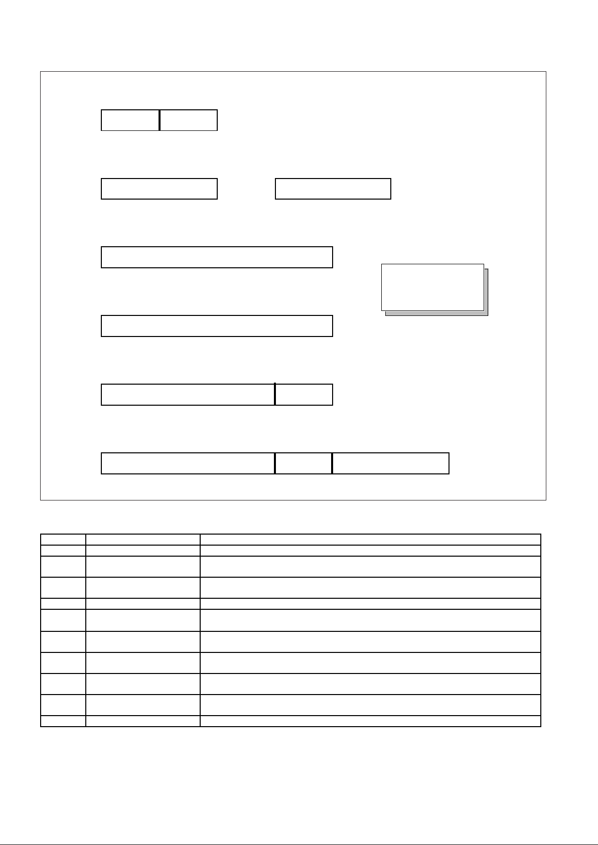
IO control
DOUT
Register
file
Address
generator
Sequencer
Microcode ROM
ALU Qshift
Multiplier Shift network
Interrupt
controller
Flags
Bus
Control
Parity
Bus
arb. Address Data
CLK
ebf
Microcode control
words to other blocks
Y bus
R bus
S bus
Ints
Faults
uAddr
C0
C1
IB
IA
X
BR
rap
sc
mov
ir
abort
uData
bf
IC A
aluv
INTAKN
BUSFAULTN
Figure 1: Architecture
MA31750
High Performance MIL-STD-1750 Microprocessor
Replaces July 1999 version, DS3748-7.0 DS3748-8.0 January 2000
Page 2

MA31750
2/42
1. ARCHITECTURE
The Dynex Semiconducor MA31750 Microprocessor is a
high performance implementation of the MIL-STD-1750A
(Notice 1) Instruction Set Architecture. Figure 1 depicts the
architectural details of the chip. Two key features of this
architecture which contribute to the overall high performance
of the MA31750 are a 32-bit shift network and a 24-bit parallel
multiplier. These sub-systems allow the MA31750 to perform
multi-bit shifts, multiplications,divisions and normalisations in a
fraction of the clock cycles required on machines not having
such resources. This is especially true of floating-point
operations, in which the MA31750 excels. Such operations
constitute a large proportion of the Digital Avionics Instruction
Set (DAIS) mix and generally a high percentage of many signal
processing algorithms, therefore having a significant impact on
system performance.
Key features include:
1) A three-bus (R, S, and Y) datapath consisting of an
arithmetic/logic unit (ALU), three-port register file, shift
network, parallel multiplier and flags block;
2) Four instruction fetch registers C0,C1, IA, and IB;
3) Two operand transfer registers DI, and DO;
4) Two address registers IC and A;
5) A state sequencer;
6) Micro-instruction decode logic.
The relationship between these functional blocks is shown
in Figure 1.
2. ADDITIONAL FEATURES
The MA31750 may be operated in one of two basic user
selectable modes. 1750A mode follows the requirements of
MIL-STD-1750A (Notice 1) and implements all of the
mandatory features of this standard. In addition, many of the
optional features such as interval timers A and B, a watchdog
timer and parity checking are included. 1750B mode, when
selected, allows the user access to a range of new instructions
and features as described in the Draft MIL-STD-1750B, Option
2. These include a range of unsigned arithmetic operations
and expanded addressing support instructions.
2.1. MIL-STD-1750 OPTIONAL FEATURES
In addition to implementing all of the required features of
MIL-STD-1750A and the Draft standard MIL-STD-1750B, the
MA31750 also incorporates a number of optional features.
Interval timers A and B as well as a trigger-go counter are
provided. Most specified XIO commands are decoded directly
on the chip and an additional set of commands, associated
with MMU and BPU operations, are also decoded on chip.
2.2. BUS ARBITRATION
The MA31750 has a number of extra control lines to allow
its use in a system utilising multiple processors. A bus request
and grant system coupled with external arbitration logic allows
common data and address buses to be used between devices.
A lock request pin is also provided to allow the processor to
maintain control of the buses when modifying areas of shared
memory.
2.3. MEMORY BLOCK PROTECTION
The basic MMU function allows write or execute protection
to be applied on 4KWord block boundaries. This may be
further resolved to 1kWord blocks by the inclusion of a Block
Protect Unit (BPU). The MA31751 can act as both an MMU
and a BPU in 1750A mode, operating with the full compliment
of 1MWord of memory. It will also support expansion to
8MWord in accordance with Draft MIL-STD-1750B.
Page 3
MA31750
3/42
3. MODES OF OPERATION
MA31750 operating modes include: (1) initialisation, (2)
instruction execution, (3) interrupt servicing, (4) fault servicing,
(5) timer operations and (6) console operation.
3.1. INITIALISATION
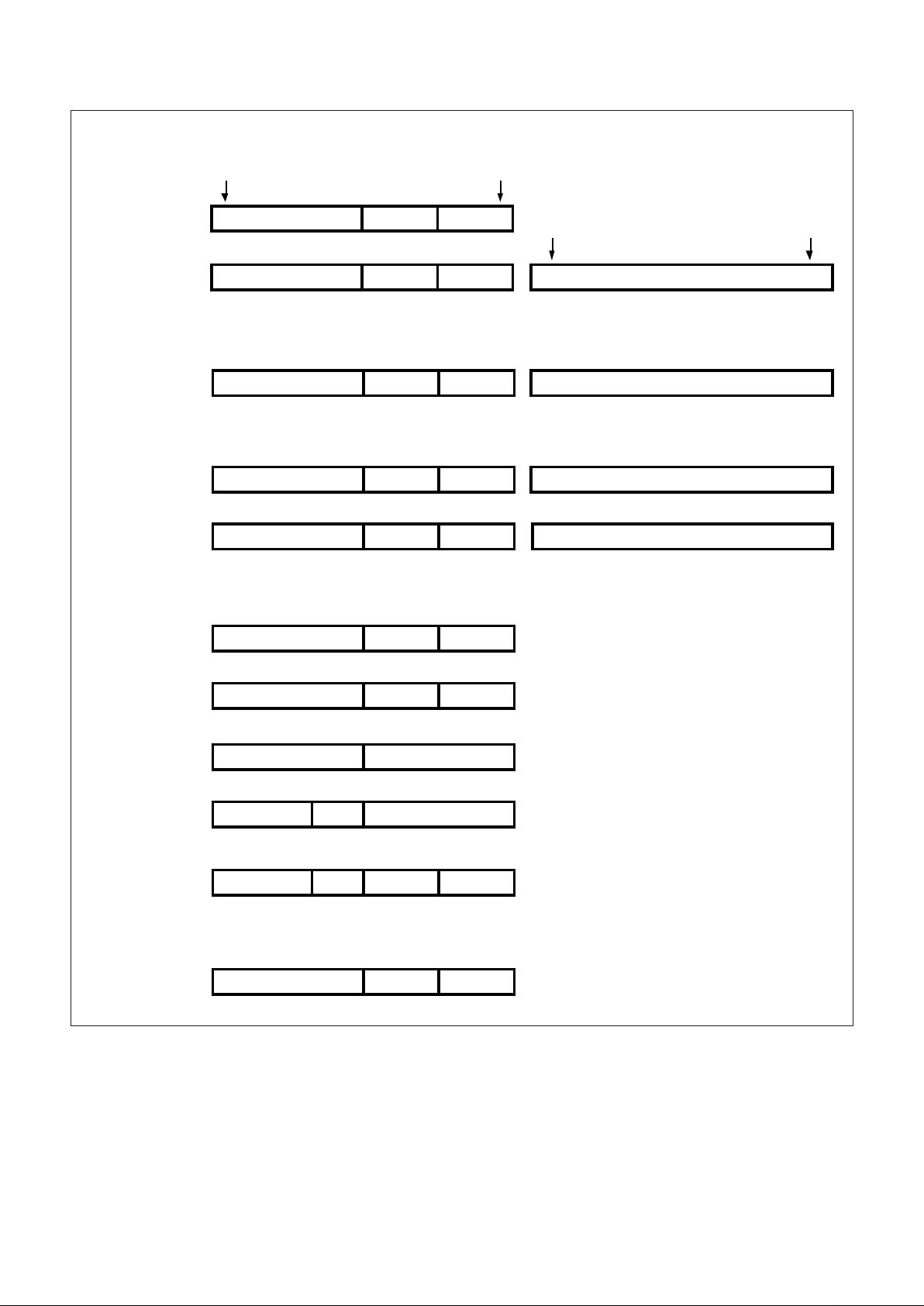
The MA31750 executes a microcoded initialisation routine
in response to a hardware reset or power-up. Figure 3 shows
a cycle-by-cycle breakdown of this routine. The operations
performed are dependent on the system configuration read by
the processor during startup. Figure 2 summarises the
resulting initialisation state.
The last action performed by the initialisation routine is to
load the instruction pipeline. Instruction fetches start at
memory location zero with AS = 0, PS = 0 and PB = 0 and will
be from the Start-Up ROM (SUR) if implemented. Whether
BIT passes or not, the processor will begin instruction
execution at this point. The system start-up code may include
a routine to enable and unmask interrupts in order to detect
and respond to a BIT failure if required.
Addr Operation
0 PIC initialised
1 A<-- 0x8410
*2 Read external configuration register from 8410H
(CONFWN asserted low)
31F 20 If BPU, N<-- 128 else N<-- 0
21 Decrement N; branch to 21 if N >= 0
4 Write internal configuration register
56 If no MMU, br to 7
13 14 15 N <-- 256
16 Decrement N
*17 Write MMU Instruction Page Register N
*18 Write MMU Operand Page Register N; branch to 16 if
N > 0
19 A <-- 0400H
1A N <-- 16
1B PBSR <-- N
1C *1D Write Memory control register to MMU with PB = N
1E Decrement N; branch if N >= 0 to 1B
7 A <-- 0
8 IC <-- A
9 Br to BIT if required
AB Br if no SUR to 00D
CD Re-init PIC
E*F Zero SW
10 32 33 Br to 011 if BIT passed (or not run)
34
35
36 Set FT bit 13
11 Init DMAE, SUREN, NPU
12
*3F8 Fetch first word from 0
*3F9 Fetch second word from 1
First instruction first cycle
* Indicates an external cycle
Figure 3: Initialization Sequence
Figure 2: Initialization State
MA31750
Instruction Counter Zero
Status Word Zero
Fault Register Zero Zero
Fault Mask Register (1750B) All ones
Pending Interrupt Register Zero
Interrupt Mask Register Zero
General Registers Undefined
Interrupts Disabled
Timers A and B Zeroed and started
Timer Reset Registers (1750B) Zero
Trigger-Go Counter Reset and started
TGON Line High
Start-Up ROM Enabled
DMA Disabled
MMU
Page Registers AL/W/E fields Zero
Page Register PPA field Logical to physical
BPU
Memory Protect RAM Zero (disabled)
Global Memory Protect Enabled
Page 4
MA31750
4/42
3.1.1. CONFIGURATION REGISTER
The system configuration register allows the MA31750 to
function with a variety of different system designs.
Implemented features such as a BPU should be indicated as
present by setting bits in an externally-implemented 16-bit
latch - see figure 4 for bit assignments. The latch must be
placed in IO space at the address defined by XIO RCW (8410)
shown in the table of XIO commands, Figure 20c. The
processor decodes this command internally and produces a
discrete output signal CONFWN which may be used as the
external register Output Enable control.
3.1.2. BUILT-IN TEST (BIT)
BIT consists of ten subroutines, as outlined in Figure 6. If
all ten subroutines execute successfully, or no BIT is selected
in the configuration word, a BIT pass is flagged (seen
externally as NPU raised high by the initialization routine). If
any part of BIT fails, a corresponding bit identifying the failed
subroutine is set in General Register R0, Fault Bit 13 is set in
the Fault register (FT) and NPU is left in the low state. Figure 6
defines the coding of BIT results in R0. In the event of such a
failure, the resulting processor reset state will be dependent on
where in BIT the error occurred and may not be the same as
that shown in figure 2. A BIT failure indication in FT will set the
level 1 interrupt request bit of the Pending Interrupt (Pl)
register. Since initialisation disables and masks interrupts, this
interrupt request will not be asserted. Any external interrupts or
faults occurring during BIT will be cleared before program
execution begins and will not be serviced.
The processor maintains an internal configuration register
which is updated from the external register during initialisation
and during the execution of a NOP/BPT (No-op/Breakpoint)
instruction. The internal configuration register is used to
control the CPU. Note that although the external register can
be read using XIO RCW, this does not affect the internal
configuration. Note: if the interrupt level/edge trigger select bit
- (bit 4) is changed in the internal register during normal
operation of the device, one or more spurious interrupts may
occur.
When in 1750B mode, the processor needs to know how
many Page Banks are implemented in the external system so
that Status Word changes can be protected properly. MILSTD-1750B allows the options 0,1,2,4,8 or 16. The actual
selection should be coded into the three configuration register
bits MMU0, MMU1 and MMU2 as shown in figure 5.
In 1750A mode, setting any of the MMU select bits
indicates the presence of an MMU, the actual code is
unimportant in this mode.
BPU selects bits 2:0 should be set to indicate how much
BPU-protected memory exists on the system. If no BPU is
present, all three bits should be zero.
Bit Function
0 MMU Select 0
1 BPU Select 0
2 1 = Console operation enabled
3 MMU Select 1
4 Interrupt sensitivity (1 = level, 0 = edge)
5 MMU Select 2
6 Parity sense (1 = odd, 0 = even)
7 1= BIT on power-up
8 1 = Start-Up ROM present
9 1 = DMA device present
10 1=1750A mode, 0=1750B mode
11 1=Instruction set expansion enabled
12 BPU Select 1
13 BPU Select 2
14-15 Reserved for future expansion
Figure 4: Configuration Word Bits
Selected bit Function
MMU2 MMU1 MMU0
0 0 0 No MMU in system
0 0 1 1 Page Bank (PB0)
0 1 0 2 Page Banks (PB0-1)
0 1 1 4 Page Banks (PB0-3)
1 0 0 8 Page Banks (PB0-7)
1 0 1 16 Page Banks (PB0-15)
1 1 X 16 Page Banks (PB0-15)
Note: In 1750A mode, setting any or all of the MMU
select bits indicates the presence of an MMU.
Figure 5: MMU Selection Bits
Test Coverage Machine
Cycles
Bit set
on fail
Temporary Registers (T0-T11) 47 7
General Registers (R0-R15) 79 7
Flags Block 18 8
Sequencer Operation and ROM
checksum
5632 9
Divide routine Quotient Shift
Network
12 10
Multiplier and ALU 13 11
Barrel shift Network 13 12
Interrupts and fault handling and
detection
17 13
Address generator block 13 14
Instruction pipeline 15 15
Note: BIT pass is indicated by all zeros
in FT bits 13,14, and 15
Figure 6: Built-In Test Coverage
Page 5
MA31750
5/42
3.2. INSTRUCTION EXECUTION
Once initialisation has been completed, the processor will
begin instruction execution. Instruction execution is
characterised by a variety of operations, each is one machine
cycle in duration (two or more system CLK periods).
Depending on the instruction being executed at the time, these
operations include: (1) internal CPU cycles, (2) instruction
fetches, (3) operand transfers, and (4) input/output transfers.
Instruction execution may be interrupted at the end of any
individual machine cycle by an interrupt or Console request.
Internal cycles are always two CLK periods long, whilst the
other cycle types are a minimum of two CLK periods extendable by inserting waitstates. In all cycles except internal
cycles, RDN, WRN, DSN and AS strobes are produced to
control the transfer and latching of data and address around
the system.
Cycle Type RD/WRN O/IN M/ION Description
Internal Cycle H L H Used to perform all CPU data manipulation operations where bus
activity is not required.
Instruction
Fetch
H L H Used to keep the instruction pipeline full with instructions and/or their
postwords. At least one instruction is always ready for execution when
the preceding instruction is completed. During jump and branch
instruction execution the pipeline is refilled by two consecutive
instruction fetches starting at the new instruction location. It is also
refilled as part of interrupt request processing.
Operand Read
Operand WriteHL
H
H
H
H
Used to read in data from the external system and to write results to the
system.
IO Read
IO Write
H
L
H
H
L
L
Input/Output transfers utilize the MIL-STD-1750 XIO and VIO
instructions. RD/WN defines the direction of the transfer. IO transfers
may be divided into three groups; those commands which are
implemented internally by the CPU, those commands which are
implemented by external system hardware and those commands
defined as illegal by MIL-STD-1750A and B.
Figure 7: External Cycle Types
3.3. IO OPERATION
The MA31750 supports a 64KWord addressing space
dedicated to IO control and communication in accordance with
MIL-STD-1750. The control line MION is asserted low when
accessing IO space (see figure 7 above for other strobe
states). One of the two commands XIO or VIO is used to
specify both data for the transfer and the port address (referred
to as an XIO Command in 1750). The CPU contains logic
which decodes all internally supported XIO commands and
generates the control signals necessary to carry out the
commanded action. In addition, the validity of a command not
implemented internally is verified. Figure 20c identifies the XIO
commands which are internally supported by the MA31750.
3.4. INTERRUPT AND FAULT HANDLING
3.4.1. STATUS WORD (SW)
Figure 8 depicts the status register format. This 16-bit word
is divided into four, 4-bit sections. Three of these sections [AS,
PS and, (1750B mode) PB] are control bits for implementing
expanded memory with an external MMU. The fourth section,
CS, is used to hold the carry, positive, zero and negative
condition flags set by the result of the previous arithmetic
operation.
CS R (PB) PS AS
0 3 4 7 8 11 12 15
Field Bits Description
CS
0
1
2
3
CONDITION STATUS
C- Carry from an addition or no
borrow from a subtraction.
P- Result > 0
Z- Result = 0
N- Result < 0
R
PB
4-7 RESERVED (=0) in 1750A mode
Page Bank Select in 1750B mode
PS 8-11 PROCESSOR STATE:
(a)- Memory access to key code
(b)- Priviledged instruction enable
AS 12-15 ADDRESS STATE:
Page register sets for expanded
memory addressing.
Figure 8: Status Word Format
Page 6
MA31750
6/42
The AS field is used during expanded memory access to
define the page register set to be used for instruction and
operand memory references. The PS field is used during
memory protect operations to define the access key used for
memory accesses. The PS field is also used during execution
of privileged Instructions - PS must be zero for such operations
to be legal. See Section 4.3 for further information on the use
of this field. The PB field is used in conjunction with the AS
field in 1750B mode to expand the number of page registers
available. Note that attempting to set AS or PB to a non-zero
value with no MMU, or setting PB to a non-zero value in 1750A
mode is illegal. This will be aborted and a fault 11 will be
generated (SW will remain unchanged).
3.4.2. PENDING INTERRUPT REGISTER (PI)
This 16-bit register is used to capture and hold interrupts
until they can be processed by microcode and user software. A
logic 1 is used to represent an active pending interrupt. The Pl
register supports three dedicated external, six user-definable
external, and seven dedicated internal interrupts. Levelsensitive interrupts are sampled on each rising CLK edge,
whilst edge sensitive interrupts are captured immediately.
Figure 10: Fault Register Bit Assignments
Figure 9: Pending Interrupt Bit Assignments
System Internal
Interrupts Interrupts
PWRD 0 (Cannot be disabled or masked)
1 Machine Error (Cannot be
disabled)
INT02 2
3 Floating-Point Overflow
4 Fixed-Point Overflow
5 Executive call (Cannot be
disabled or masked)
6 Floating-Point Underflow
7 Timer A Overflow
INT08 8
9 Timer B Overflow
INT10 10
INT11 11
IOI1 12
INT13 13
IOI2 14
INT15 15
System Internal
Faults Faults
MPROE (CPU) 0
MPROE (DMA) 1
PE (CPU memory) 2
PE (CPU IO) 3
PE (DMA) 4
EXADE or Bus 5
Timeout (CPU IO)
6 Parallel IO Transfer Error
FLT7 7
EXADE or Bus
Timeout (CPU 8
memory)
9 Illegal Instruction Opcode
10 Priviledged Instruction
11 Unimplemented Address State
Reserved 12
SYSF 13 MA31750 BIT Fail
EXADE (DMA) 14
SYSF 15
Page 7
MA31750
7/42
3.4.3. MASK REGISTER (MK)
This 16-bit register is used to store the interrupt mask.
Interrupts are masked by ANDing each mask bit with its
corresponding Pl register bit. ie. A logic zero in a given bit
position indicates that the corresponding bit in the Pl register
will be masked. Interrupts which are masked will be captured
in the Pl register but will not be acted on until unmasked.
Interrupt level zero can not be masked.
3.4.4. PRIORITY ENCODER
This encoder generates an interrupt request to the
sequencer block whenever one or more unmasked interrupts
are pending and enabled in the Pl. The highest priority
unmasked pending interrupt is encoded as a 4-bit vector. This
vector is used during interrupt servicing in order to create the
interrupt linkage and service pointers.
3.4.5. FAULT REGISTER (FT)
This 16-bit register is used to capture and hold both internal
and user implemented external faults using positive logic, i.e.,
a logic one represents a fault. Bus cycle faults are captured at
the end of each machine cycle whilst the two general purpose
faults SYSFN and FLT7N are set when the low time exceeds
the minimum pulse width. Setting any one or more faults in FT
will cause a level 1 (machine error) interrupt request. Once a
fault is set in FT, it may only be cleared via an XIO command.
In 1750B mode, a fault mask register is provided to allow
selective masking of fault conditions. Section 4 (Software
Considerations) contains further information. Figure 27 shows
the fault register assignments.
3.4.6. MEMORY FAULT PAGE AND ADDRESS REGISTERS
These registers capture the page and address information
at the end of each external cycle until a memory fault occurs.
Faults setting bits 0, 1, 2 and 8 in the fault register cause the
registers to stop latching new address information, so retaining
information about the address at which the fault occured. The
registers can be read (using the GPS defined XIOs RMFP and
RMPA). The fault register must be cleared and both memory
fault registers read before latching can restart.
The information stored in the memory fault registers is as
follows:
MFPR[0:3] MFPR[4:7] MFPR[8:10] MFPR[11]
A[0:3] PB[0:3](ASOB) Res ION
MFPR[12:15] MFAR[0:15] Note: MFPR[11] is the
AS[0:3] A[0:15] inverse of OIN.
These registers are only available if there is an MMU in the
system. If there is no MMU present, then the RMFP and RMFA
XIO commands become illegal.
The address information held in these registers can be
used to restart code after a memory fault has occurred. Bits
[6:7] of the OAS register store information on the type of
instruction which was being executed when the fault occured:
00 → branch that was taken
01 → single word instruction
10 → double word instruction
(Subtracting this value from the saved address will give the
address of the failed instruction unless it was a branch that
was taken).
3.4.7. INTERRUPT SERVICING
Nine user interrupt request inputs are provided for
programmed response to asynchronous system events. A low
on any of these inputs will be detected at the rising edge of
CLK (level sensitive interrupts only) and latched into the
Pending Interrupt (Pl) register on the falling edge of CLK at the
end of the current CPU cycle. This sequence occurs whether
interrupts are enabled or disabled or whether the specific
interrupt is masked or unmasked. More details of interrupt
operations are available in Applications Note 4.
All of the user interrupts PWRDN, INT02N - INT15N may
be programmed to be either level or edge sensitive by setting
or clearing the appropriate bit in the system configuration
register. If edge sensitivity is selected then an interrupt request
input must return to the high state before a subsequent request
on that input will be detected. If level sensitivity is selected then
holding an interrupt input low will cause a new interrupt to be
latched following each service. Note that interrupts IOI1N and
IOI2N are level sensitive only.
In order that the system may recognise when a service has
been started, an interrupt acknowledge pin is provided. During
the microcoded interrupt service routine execution, the
processor will read the Linkage Pointer address in memory.
During this operand read cycle, the processor will also assert
INTAKN low, which may be used in conjunction with AS and
address bus bits A[11:14] to reveal the priority level of the
interrupt being serviced. (A[11:14] = 0 indicates level 0
interrupt, A[11:14] = 1 indicates level 1 interrupt, and so on).
INTAKN should also be used to remove level-sensitive
interrupt requests to ensure that repeated requests are not
generated.
Linkage
Pointer 0
Service
Pointer 0
Linkage
Pointer 1
Service
Pointer 1
Linkage
Pointer 15
Service
Pointer 15
Interrupt 0
Interrupt 1
Interrupt 15
Old Interrupt
Mask
Old Status
Word
Old Instruction
Counter
CPU status at time
of interrupt
New Interrupt
Mask
New Status
Word
New Instruction
Counter
Status at start of
Service Routine
Figure 11: Interrupt Vectoring
Page 8
MA31750
8/42
When an interrupt request is latched into Pl, it is ANDed
with its corresponding mask bit in the mask register (MK).
NOTE: Interrupt level 0 is non-maskable. Any unmasked
pending interrupts are output to the priority encoder where the
highest priority is encoded as a 4-bit vector. If interrupts are
enabled and an unmasked interrupt is pending, the priority
encoder will assert an interrupt request to the sequencer. 1 or
2 extra CLKs will be inserted into the machine cycle on which
the interrupt request is asserted.
Upon completing execution of each MIL-STD-1750A or B
instruction, the sequencer checks the state of the priority
encoder interrupt request. If a request is asserted, the
sequencer branches to the microcode interrupt service
routine. This routine reads the 4-bit pending interrupt vector
and then uses this value to calculate the appropriate interrupt
linkage (old processor context save area) and service (new
context load area) pointers. Figure 11 depicts this relationship.
Figure 12 defines the pointer values.
Using the linkage and service pointers, the microcode
interrupt service routine performs the following: (1) the current
contents of the status word, mask register, and instruction
counter are saved; (2) a write status word (WSW) I/O
command is executed with an all zero data word; (3) the new
mask is loaded into MK and interrupts are disabled; (4) the
new status word is read and checked for a valid Address State
(AS[0:3]) field - If the address state is non-zero and an MMU is
not present, AS[0:3] is set to zero and fault 11 (address state
error) is set in the fault register FT); (5) a write status word
command using the new status word is performed; and (6) the
new IC value is loaded into IC, the instruction pipeline is
flushed and refilled starting at the new address, and instruction
execution begins.
[NOTE: The steps listed above represent a summary of
actions performed during interrupt servicing and do not
necessarily reflect the actual order in which these events take
place.]
If an address state fault occurs during the service routine,
interrupt level 1 will be set. This interrupt will be serviced when
interrupts are re-enabled unless it is masked by the new value
in MK.
3.4.8. FAULT SERVICING
Five user fault inputs are provided. A low on any of the
three bus-cycle-related fault inputs, EXADEN, MPROEN or
PEN, will be latched into the Fault Register (FT) on the next
falling edge of AS. A low on either of the two general purpose
fault inputs, FLT7N or SYSFN, will be latched immediately and
will be sampled into the appropriate bit of FT on the falling
edge of AS.
Any fault which sets a bit in the FT immediately causes a
level 1 pending interrupt to be entered into the PI register. This
interrupt is maskable but may not be disabled.
This interrupt will be serviced at the end of the currently
executing 1750 instruction if not masked. The microcoded
interrupt service routine reads the interrupt priority vector and
clears the bit relating to the serviced interrupt from the PI.
However, the FT retains the set fault bits until the FT is cleared
using the XIO RCFR command. (A non-destructive read of the
FT is provided by the XIO RFR command.) Anti-repeat logic
between the FT and the PI prevents the same fault being
latched and serviced twice. However, as all FT bits are ORed
together and input to PI bit 1, this also prevents any other faults
being serviced until the fault register has been cleared. It is
imperative, therefore, that the fault service routine executes a
RCFR XIO before exiting. Different types of faults are serviced
slightly differently as follows:
3.4.8.1. MPROEN and EXADEN
If MPROEN and/or EXADEN are low on a falling clock
edge with AS and DSN high (see figure 23a), the processor will
wait in this state. If either fault input remains low during two
falling edges of TCLK, the cycle is forced to complete but RDN/
WRN and DSN are inhibited (see figure 24b). This allows the
processor to prevent erroneous accesses. An access fault will
be registered as AS falls at the end of the cycle.
3.4.8.2. PEN
External parity errors are latched into the FT on the falling
edge of AS. The fault bit set is dependant upon the type of
transfer taking place (memory, IO or DMA).
3.4.8.3. FLT7N and SYSFN
These faults are latched immediately, but are not sampled
into the fault register until the following falling edge of AS.
3.4.9. PARITY GENERATION AND CHECKING
The MA31750 features on-chip parity generation and
checking on all data bus transfers. Data generated by the
processor has a parity bit attached to it to allow external logic
to verify write transfers. On read transfers, the processor will
check the incoming parity (if enabled) and will generate the
appropriate parity error fault if detected. However, the data to
be checked is only available as DSN rises at the end of the
cycle so the error flag is generated and latched in the cycle
following the erroneous cycle. Parity checking may be
Interrupt
No.
LP
AddressSPAddress
PWRD 0 20 21
ME 1 22 23
INT02 2 24 25
FI.P o/f 3 26 27
Fx.P o/f 4 28 29
BEX 5 2A 2B
FI.P u/f 6 2C 2D
Timer A 7 2E 2F
INT08 8 30 31
Timer B 9 32 33
INT10 10 34 35
INT11 11 36 37
IOI1 12 38 39
INT13 13 3A 3B
IOI2 14 3C 3D
INT15 15 3E 3F
Note: Addresses (in hex) are in operand space
Figure 12: Interrupt Pointer Address
Page 9

MA31750
9/42
disabled when operating with devices which do not support
parity generation by asserting the DPARN (Disable Parity)
input low. The checking polarity (odd or even) is selectable
with Configuration Register bit 6.
3.5. TIMER OPERATIONS
The MA31750 implements interval timers A and B, a
trigger-go counter, and a bus fault timer. A discussion of each
follows:
3.5.1. TIMERS A AND B
Two general-purpose, 16-bit timers are provided in the
processor. Timer A is clocked by the TCLK input; timer B is
clocked by an internally generated TCLK/10. The divider
circuit is reset when Timer B is reset to give deterministic
processor operation. MIL-STD-1750 requires TCLK to be a
100kHz pulse train. If allowed to overflow, timers A and B will
set level 7 and level 9 interrupt requests respectively. Each
timer can be read, loaded, started and stopped by using XIO
commands as identified in figure 20c.
Each timer has associated with it a reset register from
which the timer is automatically loaded following a software
reset or overflow. These registers are initially loaded with zero
but may be reloaded from software (using the XIO instructions
OTA and OTB) to provide greater control over the count
period.
The MA31750 timers A and B will be disabled when the
device enters Console mode, as required by MIL-STD-1750A
Notice 1.
3.5.2. TRIGGER-GO COUNTER
This 16-bit counter is clocked by the TCLK input and is
typically used as a system “watchdog” timer. It is enabled
during system initialisation and may be preset under software
control to give a wide range of timeout intervals. In order that
the count period may be controlled, a reset register is
provided. On reset, this register is loaded with zero, but can be
reloaded under software control to take any value between 0
and FFFF
16
(a value of zero gives the maximum count period).
This allows the timeout period to be varied between 20us and
0.65s. Note that there is no value which disables the timer.
The counter is incremented on each TCLK falling edge.
Whenever the trigger-go counter overflows, TGON drops low
and remains low until the counter is reloaded from the reset
register via the GO internal XIO command. TGON low would
typically be used to initiate a user-defined system recovery
action such as a system reset.
3.5.3. BUS FAULT TIMER
All bus operations are monitored to ensure timely
completion. A hardware timeout circuit is enabled at the start of
each memory and l/O transfer (DSN high-to-low transition) and
is reset upon receipt of the external ready (RDYN) signal. If
this circuit fails to reset within a minimum of one TCLK period
or a maximum of two TCLK periods, either bit 8 (if the
transaction is with memory) or bit 5 (if the transaction is with l/
O) of the Fault Register (FT) is set. This sets Pending Interrupt
level 1 and causes the strobes to be suppressed and the
current bus cycle to be aborted. The MIL-STD-1750 instruction
is aborted, and control passes to the level 1 interrupt service
routine (if the level 1 interrupt is unmasked). The timeout
mechanism is disabled and reset if DTON is asserted low.
3.6. CONSOLE OPERATION
The MA31750 is capable of interfacing directly to an
external console, allowing the developer to: examine and
change the contents of internal registers, memory and IO
devices; single step code and halt the processor. Applications
Note 3 provides a full description of the Console interface, its
implementation and operation.
3.7. MULTIPROCESSOR SUPPORT
Once initialisation has been completed, the processor will
begin instruction execution by executing a sequence of microinstructions, each one machine cycle (two system clock
periods) long. Each machine cycle may perform either an
internal or an external operation; if the operation is purely
internal then the system busses will not be in use and may be
reassigned to another processor.
An external machine cycle (indicated by REQN low during
the second half of the previous cycle) will cause the processor
to stall upon completion of the current microcycle, awaiting
GRANTN asserted low. Whilst GRANTN is high the busses
remain undriven.
In simple, single processor systems which use no DMA
devices the GRANTN line should be tied to GND to allow the
processor to retain control of the busses. The LOCKN and
REQN pins can be left open-circuit in this case. Applications
Note 11 provides further information for designers of systems
with more than one bus master.
4. SOFTWARE CONSIDERATIONS
4.1. OPERATING MODES
The MA31750 is capable of being operated in one of two
basic modes as previously mentioned. These are described in
detail below:
4.1.1 1750A MODE
1750A mode is a full implementation of MIL-STD-1750A
(Notice 1) and includes some of the optional features
mentioned in this standard.
4.1.2 1750B MODE
1750B mode is an implementation of the proposed MILSTD-1750B, Option 2, Draft of 17th July 1988. This mode
extends the basic 1750A mode operation. Note that the
transcendental functions SIN, COS, LN etc. (Option 3 of MILSTD-1750B) are not supported. Features new to MIL-STD1750B which are in violation of MIL-STD-1750A are only
enabled in 1750B mode. The additional instructions available
in 1750B mode are detailed in figure 20b.
4.2. ACCESSING IO USING XIO AND VIO COMMANDS
MIL-STD-1750 defines a 64KWord addressing space
which is available exclusively for accessing IO resources. Two
special commands, XIO and VIO, are provided as part of the
instruction set for accessing this space. Port addresses are
specified as a 16-bit Command word which is supplied as a
parameter to the XIO/VIO instruction. The MSB of the
Command word indicates the direction of data transfer
between the port and the register specified in the XIO
command (a 1 in the MSB indicates that the port is being read,
whilst 0 indicates a write to the port).
Page 10

MA31750
10/42
Figure 13: XIO Command Channel Grouping
XIO command addresses are grouped by the Standard
according to function. Certain groups are ‘reserved’ and must
not be implemented. Attempts to read or write these areas will
be prevented by the processor and a fault will be logged in the
fault register. Other groups are designated ‘spare’ and may be
implemented as required by the system designer. Note,
however, that there is a third group which access system
resources such as MMU page registers and interrupt control
registers which are not available to the user to implement. A
summary of the XIO map is provided in figure 13, whilst the
detailed list of implemented command addresses is shown in
Figure 20c.
The VIO (Vectored IO) command allows a number of IO
operations to be executed in a sequence from a table.
Applications Note 8 gives further information on the use of this
command.
Both XIO and VIO are priveleged commands and as such
can only be executed when the Status Word PS field is zero.
4.3. PROCESSOR STATE AND PRIVILEGED
INSTRUCTIONS
The Processor State is defined by a 4-bit value held in the
processor Status Word. If the value is made non-zero then
attempts to execute the commands XIO, VIO or LST will be
aborted and a fault will be raised. This is intended to deny
direct access to the hardware from user applications (running
in PS≠0), whilst allowing the Operating System (operating with
PS=0) access to the system IO and interrupt resources.
If an MMU is present on the system the PS field is used in
conjunction with the page register Access Key field to provide
a further level of protection to the system. When PS=0 access
is granted to all pages, irrespective of their key value. If PS is
non-zero, access is only permitted if the Access Key is equal to
the PS value, or the Access Key is 15. Access Key 15 should
be applied to a shared area of code or data, and is accessable
to all PS values.
Output Input Usage
0000-03FF 8000-83FF PIO
0400-1FFF 8400-9FFF Spare
2000-20FF A000-A0FF CPU and auxiliary register control
2100-2FFF A100-AFFF Reserved
3000-3FFF B000-BFFF Spare
4000-40FF C000-CFFF CPU and auxiliary register control
4100-4CFF C100-CCFF Reserved
4D00-4FFF CD00-CFFF Extended memory protect RAM
5000-50FF D000-D0FF Memory protect RAM
5100-51FF D100-D1FF MMU Instruction Page Registers
5200-52FF D200-D2FF MMU Operand Page Registers
5300-7FFF D300-FFFF Spare
4.4. USING START-UP ROM
The transition between code execution from Start-up ROM
and system RAM must be made with care. If a system overlays
RAM with the Start-Up ROM and the transition is made by
simply executing XIO DSUR from the ROM, then the
instruction pipeline will contain the value stored in the ROM
location immediately following the XIO DSUR command. This
value will be treated as an instruction and the processor will
attempt to execute it. In such cases, it is recommended that
DSUR be followed by an unconditional branch instruction with
offset, i.e. the BR instruction. An alternative approach is simply
to jump to a portion of RAM not overlaid by the Start-Up ROM
and execute DSUR from RAM.
4.5. USING SOFTWARE TIMERS A AND B
The MA31750 implements the two software timers, A and
B as defined in the MIL-STD 1750A specification. These are
general purpose timers which are clocked at 100kHz and
10kHz respectively, giving clock ‘tick’ intervals of 10us and
100us respectively. They may be started using the XIO TAS
and XIO TBS instructions, and stopped using XIO TAH and
XIO TBH. If a timer is allowed to overflow (FFFF
16
- 000016) it
will generate pending interrupt levels 7 (A) or 9 (B).
In 1750B mode each timer has associated with it a reset
register which may be loaded with any 16-bit value from
software. If a timer is allowed to overflow, an automatic reset
will take place which will reload the timer with the value held in
its on-chip reset register, provided that the timer had
previously been loaded using XIO OTA/OTB. If this is not the
case, then the timers will reset to zero on overflow. Each of the
reset registers is initialised to zero but may be changed using
XIO OTAR or XIO OTBR.
4.6. FAULT MASK REGISTER
A fault mask register is accessible in 1750B mode. Its
function is similar to that of the Interrupt Mask register and
allows selective enabling and disabling of all bits in the Fault
Register. All faults are maskable. Setting a bit in this register
allows the corresponding fault bit to be seen by the system.
The mask register is loaded with FFFF
16
on initialisation.
4.7. GENERAL REGISTERS R0-R15
There are 16 general purpose registers defined by MILSTD-1750; each is 16-bits wide. Adjacent registers may be
concatenated to provide storage for the larger data formats
(Double Integer and Float - 32-bit; Extended Float - 48-bit).
The first register in the set stores the most significant data
word and is the register specified when referring to the value.
Wrap-around occurs between R15 and R0.
Although generally all registers are the same, certain
registers are notionally assigned to particular tasks, see figure
15.
Page 11
MA31750
11/42
4.8. MIL-STD-1750 DATA TYPES
The MA31750 fully supports 16-bit fixed-point singleprecision, 32-bit fixed-point double-precision, 32-bit floatingpoint, and 48-bit extended precision floating- point data types.
Figure 16 depicts the formats of these data types.
All numerical data is represented in two’s complement
form. Floating-point numbers are represented by a fractional
two’s complement mantissa with an 8-bit two’s complement
exponent. All floating-point operands are expected to be
normalised. If not normalised, the results from an instruction
are not defined.
4.9. MIL-STD-1750 ADDRESSING MODES
The MA31750 supports the eight basic addressing modes
specified in MIL-STD-1750A. These addressing modes are
depicted in Figure 18 and are defined below. In binary
operations one operand is assumed to be in a register
(specified as part of the opcode) whilst the second operand
(the Derived Operand, DO) is taken from a source which is
dependent upon the addressing mode, see figure 17. Many
adddressing modes may be specified as indexable: the index
register may be any of the general purpose registers R1-R15
(if 0 is specified then the non-indexable form is used). For
Base Relative addressing modes the first operand is fixed as
part of the instruction (either R0 for Double Integer operations,
or R2 for Single Integer operations).
4.10. MEMORY ADDRESSING CAPABILITY
In accordance with MIL-STD-1750A, the MA31750 can
access a 64KWord address space directly. With the addition of
a single external Dynex Semiconductor MA31751 chip,
configured as a Memory Management Unit (MMU), this
address space may be expanded to 1MWord (1750A mode) or
8MWord (1750B mode). The MA31751 data sheet gives
further information on the MMU/BPU chip and on the memory
management scheme employed. Note that whilst one MMU
can be used to provide the full range of physical addresses to
the system memory, the logical addressing capability may also
be expanded by adding further MMU devices up to a maximum
of 16.
Figure 14: Register Set Model
R0
R1
R2
R3
R4
R5
R6
R7
R8
R9
R10
R11
R12
R13
R14
R15
Status Word (SW)
Instruction Counter (IC)
Fault Register (FT)
Fault Mask (1750B only)
Pending Interrupt (PI)
Interrupt Mask (MK)
Timer A
Timer A reset (1750B only)
Timer B
Timer B reset (1750B only)
Trigger-Go Reset Register
Configuration
Register(s) Notional Use or Restriction on Use
R0 Cannot be used as an index register
With R1: Implied register in Double mode Base Relative addressing
R2 Implied register in Single mode Base Relative addressing
R3-R11 General purpose
R12-R15 Base relative registers
R15 Stack pointer in PSHM and POPM operations
Figure 15: General Register Usage
Page 12
MA31750
12/42
Figure 16: Data Formats
Single Precision Fixed-Point
Byte
Double-Precision Fixed-Point
Floating Point
Extended Precision Floating Point
Value
015
Mantissa (Most significant) Mantissa (Least Sig.)
Exponent
0 2324 3132 47
Mantissa Exponent
02331
Upper byte Lower byte
015
Unsigned value
031
Value
031
Unsigned value
015
Unsigned Double Precision Fixed-Point (1750B)
Unsigned Single Precision Fixed-Point (1750B)
MSB LSB MSB LSB
MSB LSB MSB LSB
MSB LSB
MSB LSB
MSB LSB MSB LSB
MSB LSB MSB LSB MSB LSB
Note: All values are
Signed 2s complement
unless shown as
unsigned.
24
Mode Name Derived Operand
R Register Direct The operand is contained in a regular specified by the instruction.
D, DX Memory Direct The instruction postword (plus RX if RX ≠ 0), contains the memory address of the
operand.
I, IX Memory Indirect The instruction postword (plus RX if RX ≠ 0) contains the address of the address
which holds the operand.
IM, IMX Immediate Long The instruction postword (plus RX if RX ≠ 0) holds the operand.
ISP Immediate Short Positive The operand value is specified as part of the instruction. (ISP specifies values
between 0001H and 0010H, ISN specifies values between FFFFH and FFEFH).
ISN Immediate Short Negative The operand value is specified as part of the instruction. (ISP specifies values
between 0001n and 0010n, ISN specifies values between FFFFn and FFEFn).
ICR Instruction Counter
Relative
A 2s-complement, 8-bit displacement which is sign-extended and added to the
Instruction counter to provide an offset of -128 to +127.
B Base Relative Data at address given by: contents of specified base register (R12-R15, specified
by opcode), plus unsigned 8-bit displacement field from opcode.
BX Base Relative Indexed Data at address given by contents of specified base register (R12-R15, specified
by opcode), plus contents of RX register if RX ≠ R0
S Special See instruction for details.
Figure 17: Address Mode Summary
Page 13
MA31750
13/42
OC RA
0 7 8 11 12
15
OC RA
0 7 8 11 12 15
RX = 0 (Non-indexed)
RX ≠ 0 (Indexed)
OC RA
0 7 8 11 12 15
RX = 0 (Non-indexed)
RX ≠ 0 (Indexed)
OC RA
0 7 8 11 12 15
OC RA
0 7 8 11 12 15
RX = 0 (Non-indexed)
RX ≠ 0 (Indexed)
OC RA
0 7 8 11 12
15
OC RA
0 7 8 11 12
15
OC
0 7 8
15
OC
0 7 8
15
OC
OCX
0 7 8 11 12
15
RX = 0 (Non-indexed)
RX ≠ 0 (Indexed)
OC S1
0 7 8 11 12
15
RB
RX
RX
OCX
RX
I
I
D
DU
S2
RX
BR'
BR'
BR' = BR - 12
5 6
5 6
A
A
I
I
16 31
31
31
3116
16
16
Legend
OC = Operation Code
RA = Destination Register
RB = Source Register
RX = Index Register
A = Address (logical)
OCX = Extension to Operation Code
I = Immediate Data
D = Displacement
BR' = Base Register Reference
DU = Displacement (positive)
S1, S2 = Special Code
FORMAT
1. Register Direct
"R"
2. Memory Direct
"D"
"DX"
3. Memory Indirect
"I"
"IX"
4. Immediate Long
a. Not indexable
"IM"
b. Indexable
"IM"
"IMX"
5. Immediate Short
a. Positive
"ISP"
b. Negative
"ISN"
6. IC Relative
"ICR"
7. Base Relative
a. Not Indexable
"B"
b. Indexable
"B"
"BX"
8. Special
"S"
MODE MSB
LSB
INSTRUCTION
MSB LSB
POSTWORD
Figure 18: Addressing Modes
Page 14

MA31750
14/42
5. PERFORMANCE
5.1. BENCHMARKING
Figure 20a defines the number and type of machine cycles
associated with each MIL-STD-1750 instruction. This
information may be used when benchmarking MA31750
performance. The Digital Avionics Instruction Set (DAIS) mix,
which defines a typical frequency of occurrence for MIL-STD1750A instructions, is used here for this purpose.
One problem with the DAIS mix is that it does not reflect the
impact of data dependencies on system performance. E.g. a
multiplication in which the operand is zero may be performed
much faster than one with two non-zero operands.
Realistic benchmarks must therefore take both the
instruction mix and data dependencies into account. To this
end, machine cycle counts in figure 20a which have data
dependencies are annotated with either an “a” or “wa” suffix.
An “a” suffix reflects an average number of machine cycles
(where each of several possibilities is equally likely) and a “wa”
suffix reflects a weighted average number of machine cycles
(where some data possibilities are more likely than others).
Weighted averages are only applicable to floating-point
operations. Normalisation and alignment operations are also
represented. Figure 19 shows MA31750 throughput, at
various frequencies and wait states, for the floating point DAIS
mix.
5.2. EXPANDED MEMORY PERFORMANCE
The inclusion of an MMU (Memory Management Unit) will
degrade the throughput performance of the processor in two
ways. Firstly, each memory access will have an additional
overhead associated with the formation of the extended
address from the MMU. This may require that the processor
inserts wait states to lengthen each external cycle. Secondly,
the MMU itself may require that some ‘housekeeping’ work be
done by the processor, which will lengthen the program
execution time. There are no widely accepted benchmarks
which may be used to measure the resultant decrease in
throughput.
Waitstates
Performance (MIPS)
0
0.5
1
1.5
2
2.5
3
3.5
01234
25MHz
20MHz
15MHz
10MHz
5MHz
Figure 19: Throughput (MIPS) with Waitstates
Page 15

MA31750
15/42
5.3. INSTRUCTION SUMMARY
OPERATION Mnem. Format Opcode
(Ext)
Memory
cycles
Internal
Cycles
SINGLE LOAD/STORE
Single Precision Load L R R 8 1 1 0
LB B 0X 2 1
LBX BX 4X 0 2 1
LISP ISP 82 1 0
LISN ISN 83 1 0
L D,DX 80 3 0
LIM IM,IMX 85 2 0
LI I,IX 84 4 0
Double-Precision Load DLR R 87 1 0
DLB B 0X 3 1
DLBX BX 4X 1 3 1
DL D,DX 86 4 0
DLI I,IX 88 5 0
Single-Precision Store STB B 0X 2 0
STBX BX 4X 2 2 1
ST D,DX 90 3 0
STI I,IX 94 4 0
Store Non-Negative Constant STC D,DX 91 3 0
STCI I,IX 92 4 0
Double-Precision Store DSTB B 0X 3 0
DSTX BX 4X 3 3 1
DST D,DX 96 4 0
DSTI I,IX 98 5 0
Load Multiple Registers LM D,DX 89 3+n 0
Store Multiple Registers STM D,DX 99 2+n 1
COMPARE
Single-Precision Compare CR R F1 1 0
CB B 3X 2 1
CBX BX 4X C 2 1
CISP ISP F2 1 1
CISN ISN F3 1 0
C D,DX F0 3 0
CIM IM 4A A 2 0
Compare Between Limits CBL D,DX F4 4 2.7a
Double-Precision Compare DCR R F7 1 0
DC D,DX F6 4 0
BYTE
Load From Upper Byte LUB D,DX 8B 3 1
LUBI I,IX 8D 4 1
Load From Lower Byte LLB D,DX 8C 3 0
LLBI I,IX 8E 4 0
Store Into Upper Byte STUB D,DX 9B 4 0
SUBI I,IX 9D 5 0
Store Into Lower Byte STLB D,DX 9C 4 1
SLBI I,IX 9E 5 1
Exchange Bytes in Register XBR S EC 1 0
Figure 20a: Instruction Summary
Page 16

MA31750
16/42
OPERATION Mnem. Format Opcode
(Ext)
Memory
cycles
Internal
Cycles
Figure 20a (continued): Instruction Summary
INTEGER ARITHMETIC
Single-Precision Integer Add AR R A 1 1 0
AB B 1X 2 1
ABX BX 4X 4 2 1
AISP ISP A2 1 0
A D,DX A0 3 0
AIM IM 4 A 1 2 0
Increment Memory by a Positive
Integer
INCM D,DX A3 4 0
Single-Precision Absolute Value A B S R A 4 1 1.5a
Double-Precision Absolute
Value
DABS R A 5 1 1.5a
Double-Precision Integer Add DAR R A 7 1 0
DA D,DX A6 4 0
Single Precision Integer Subtract SR R B1 1 0
SBB B 1X 2 1
SBBX BX 4X 5 2 1
SISP ISP B2 1 1
S D,DX B0 3 0
SIM IM 4 A 2 2 0
Decrement Memory by a Positive
Integer
DECM D,DX B3 4 0
Single-Precision Negate NEG R B 4 1 1
Double-Precision Negate DNEG R B5 1 1
Double-Precision Integer
Subtract
DSR R B 7 1 0
DS D,DX B6 4 0
Single-Precision Integer Multiply
with 16-Bit Product
MSR R C1 1 2
MISP IS P C2 1 2
MISN ISN C3 1 3
MS D,DX C0 3 2
MSIM IM 4A 4 2 2
Single-Precision Integer Multiply
with 32-Bit Product
MR R C5 1 1
MB B 1X 2 2
MBX BX 4X 6 2 2
M D,DX C4 3 1
MIM IM 4 A 3 2 1
Double-Precision Integer Multiply DMR R C7 1 16.5a
DM D,DX C6 4 16.5a
Single-Precision Integer Divide
with 16-Bit Dividend
DVR R D1 1 23.5a
DISP ISP D2 1 23.5a
DISN ISN D3 1 23.5a
DV D,DX D0 3 23.5a
DVIM IM 4 A 6 2 23.5a
Single-Precision Integer Divide
with 32-Bit Dividend
DR R D5 1 28a
DB R 1X 2 29a
DBX BX 4X 7 2 29a
D D,DX D4 3 28a
DIM IM 4 A 5 2 28a
Double-Precision Integer Divide DDR R D7 1 41 a
DD D,DX D6 4 41a
Page 17

MA31750
17/42
OPERATION Mnem. Format Opcode
(Ext)
Memory
cycles
Internal
Cycles
LOGICAL
Inclusive Logical-OR ORR R E1 1 0
ORB B 3X 2 1
ORBX BX 4X F 2 1
OR D,DX E0 3 0
ORIM IM 4 A 8 2 0
Logical-AND ANDR R E 3 1 0
ANDB B 3X 2 1
ANDX BX 4X E 2 1
AND D,DX E2 3 0
ANDM IM 4A 7 2 0
Exclusive Logical-OR XORR R E5 1 0
XOR D,DX E4 3 0
XORM IM 4A 9 2 0
Logical NAND NR R E7 1 0
N D,DX E6 3 0
NIM IM 4A B 2 0
Set Bit SBR R 5 1 1 0
SB D,DX 50 4 0
SBI I,IX 52 5 0
Reset Bit RBR R 54 1 0
RB D,DX 53 4 0
RBI I,IX 55 5 0
Test Bit TBR R 57 1 0
TB D,DX 56 3 0
TBI I,IX 58 4 0
Test and Set Bit TSB D,DX 59 2 2.5a
Set Variable Bit SVBR R 5A 1 0
Reset Variable Bit RVBR R 5C 1 0
Test Variable Bit TVBR R 5E 1 0
Store Register Through Mask SRM D,DX 97 4 1
JUMP/BRANCH
Jump on Condition JC D,DX 70 3a 0
JCI I,IX 71 3.5a 0
Jump to Subroutine JS D,DX 72 2 1
Subtract One and Jump SO J D,DX 73 3a 0
Branch Unconditionally B R ICR 74 2 1
Branch if Equal to (Zero) BEZ ICR 75 2a 0
Branch if Less than (Zero) BLT ICR 76 2a 0
Branch to Executive BEX S 7 7 11 14
Branch if Less than or Equal to
(Zero)
BLE ICR 7 8 2a 0
Branch if Greater than (Zero) BGT I CR 79 2a 0
Branch if Not Equal to (Zero) BNZ ICR 7A 2a 0
Branch if Greater than or Equal to
(Zero)
BGE ICR 7B 2a 0
Figure 20a (continued): Instruction Summary
Page 18

MA31750
18/42
OPERATION Mnem. Format Opcode
(Ext)
Memory
cycles
Internal
Cycles
STACK
Stack IC and Jump to Subroutine SJS D,DX 7E 3 1
Unstack IC and return from
Subroutine
URS S 7F 3 1
Pop Multiple registers off the
Stack
POPM S 8F 1+n (n=0 to
15)
4
Push Multiple Registers onto the
Stack
PSHM 5 9F 1+n (n=0 to
15)
8
Figure 20a: Instruction Summary
EXTENDED PRECISION
Extended-Precision FloatingPoint Load
EFL D,DX 8 A 5 0
Extended-Precision FloatingPoint Store
EFST D,DX 9A 5 0
Floating-Point Absolute Value of
Register
FABS R AC 1 2wa
Floating-Point Negate Register FNEG R BC 1 3wa
Floating-Point Compare FCR R F9 1 3.7wa
FCB B 3X 3 3.7wa
FCBX BX 4X D 3 3.7wa
FC D,DX F8 4 3.7wa
Extended-Precision FloatingPoint Compare
EFCR R FB 1 4wa
EFC D,DX FA 5 2wa
Floating-Point Add FAR R A 9 1 7wa
FAB B 2X 3 8.5wa
FABX BX 4X 8 3 8.5wa
FA D,DX A8 4 8.5wa
Extended-Precision FloatingPoint Add
EFAR R A B 1 21wa
EF A D,DX A A 5 20wa
Floating-Point Subtract FSR R B 9 1 9wa
FSB B 2X 3 10wa
FSBX BX 4X 9 3 10wa
FS D,DX B8 4 9wa
Extended-Precision FloatingPoint Subtract
EFSR R B B 1 23wa
EFS D,DX BA 5 22wa
Floating-Point Multiply FMR R C9 1 1
FMB B 2X 3 2
FMBX BX 4X A 3 2
FM D,DX C8 4 1
Extended-Precision FloatingPoint Multiply
EFMR R CB 1 33wa
EFM D,DX CA 5 32wa
Floating-Point Divide FDR R D9 1 42.8wa
FDB B 2X 3 43.8wa
FDBX BX 4X B 3 43.8wa
FD D,DX D8 4 42.8wa
Extended-Precision FloatingPoint Divide
EFDR R DB 1 112.6wa
EFD D,DX DA 5 112.6wa
Page 19

MA31750
19/42
OPERATION Mnem. Format Opcode
(Ext)
Memory
cycles
Internal
Cycles
CONVERT
Convert Floating-Point to 16-Bit
Integer
FIX R E8 1 7.1a
Convert 16-Bit Integer to
Floating-Point
FLT R E 9 1 3
Convert Extended-Precision
Floating-Point to 32-Bit Integer
EFIX R EA 1 8.5a
Convert 32-Bit Integer to
Extended-Precision FloatingPoint
EFLT R EB 1 9
SHIFT
Shift Left Logical SL L R 60 1 0
Shift Right Logical SRL R 61 1 0
Shift Right Arithmetic SRA R 62 1 0
Shift Left Cyclic SLC R 63 1 0
Double Shift Left Logical DSLL R 6 5 1 0
Double Shift Right Logical DSRL R 66 1 0
Double Shift Right Arithmetic DSRA R 67 1 0
Double Shift Left Cyclic DSLC R 68 1 0
Shift Logical, Count in Register SLR R 6A 1 2
Shift Arithmetic, Count in
Register
SAR R 6B 1 5a
Shift Cyclic, Count in Register SCR R 6C 1 2
Double Shift Logical, Count in
Register
DSLR R 6 D 1 2
Double Shift Arithmetic, Count in
Register
DSAR R 6E 1 5
Double Shift Cyclic, Count in
Register
DSCR R 6F 1 2
I/O (See I/O Command
Summary)
Execute I/O XIO** IM,IMX 48 3 4.3a
Vectored I/O (n transfers) VIO** D,DX 49 *** ***
SPECIAL
Move Multiple Words, Memoryto-memory (n-words moved)
MOV S 93 1+2n 7
Exchange Words in Registers XWR R ED 1 2
Load Status LST** D,DX 7D 6 1
LSTI** I,IX 7C 7 1
No Operation NOP S FF 00 1 2
Break Point BPT S FF FF 1 6
Figure 20a (continued): Instruction Summary
Page 20

MA31750
20/42
OPERATION Mnem. Format Opcode
(Ext)
Memory
cycles
Internal
Cycles
1750B MODE INSTRUCTIONS
The following instructions may
only be executed in 1750B mode
and are illegal in 1750A
'LONG' LOADS AND STORES
Long Load Single LSL S CC 3 11
Long Load Double LDL S CD 4 20
Long Load Extended Precision
Floating-Point
LEFL S CE 5 27
Long Store Single LSS S DC 4 9
Long Store Double LDS S DD 6 16
Long Store Extended Precision
Floating-Point
LEFS S DE 8 23
UNSIGNED ARITHMETIC
Unsigned Integer Add UAR R AD 1 4
UA D,DX AE 3 4
Unsigned Integer Subtract USR R BD 1 4
US D,DX BE 3 4
Unsigned Integer Compare UCR R FC 1 5
UC D,DX FD 3 5
UCIM IM 4A 0 2 5
BYTE LOADS AND STORES
Load Byte LBY S BF 2 3
Load Byte With Increment LBYI S AF 2 3
Store Byte SBY S DF 2 3
Store Byte With Increment SBYI S CF 2 3
BIT OPERATION
Search First Bit Set SFBS R 95 1 3.75a
Notes:
a Average if more than one alternative exists.
wa Weighted average where data dependency exists.
** Privileged instruction - illegal if PS≠0.
*** VIO execution time dependent on number and type of transfer.
Figure 20b: MIL-STD-1750B Instruction Summary
Page 21

MA31750
21/42
5.4 I/O COMMAND SUMMARY
Implemented in CPU,
1750B mode only.
Output Timer A Reset Reg. OTAR
4002 No
Output Timer B Reset Reg. OTBR
400F No
Input Timer A Reset Register
2
ITAR
C002 No
Input Timer B Reset Register
2
ITBR
C00F No
Set Fault Mask SFMK
2006 No
Write Page Bank Select WPBS
200F No
Read Page Bank Select RPBS
A00C No
Read Fault Mask RFMK
A006 No
Implemented in BPU
Memory Protect Enable
3
MPEN
4003 Yes
Load Memory Protect RAM 3 LMP
50XX Yes
Read Memory Protect RAM
3
RMP
D0XX Yes
Load Ext Mem. Protect RAM
3,5
LXMP
4XXX Yes
Read Ext. Mem. Protect RAM
3,5
RXMP
CXXX Yes
Implemented in MMU
Write Instruction Page Reg.
3
WIPR
51XY Yes
Write Operand Page Reg.
3
WOPR
52XY Yes
Read Instruction Page Reg.
3
RIPR
D1XY Yes
Read Operand Page Reg.
3
ROPR
D2XY Yes
Implemented in Console
6
Console Data Output
4
CO
4000 Yes
Console Command
4
CC
8402 Yes
Console Data Input
4
CI
C000 Yes
Reserved by GPS
(Unavailable to the user)
Initialise Interrupt Logic PINIT
0403 No
Set NPU RNPU
040A No
Write Internal config word WCW
040C No
Write Memory Config. Reg. WMCR
0400 Yes
FMCR FMCR
A010 No
Spare and Reserved Addresses
Output Input
04XX-1FXX 84XX-9FXX
Spare
21XX-2fXX A1XX-AFXX
Reserved
30XX-3FXX B0XX-BFXX
Spare
41XX-4FXX C1XX-CFXX
Reserved
53XX-7FXX D3XX-FFXX
Spare
1
External cycles output on the address bus
2
GPS defined 1750B XIO’s
Reserved Addresses
3
Command illegal if device not implemented in config word
4
External cycle needing external ready generation
5
Only implemented in 1750B
6
The address 4001 and C001 are implemented but have no
effect in the 31750.
Figure 20c: Internal I/O Command Summary
Ope ra t ion Mnem Code Ex t
1
Implemented in CPU
1750A or B mode
Set Interrupt Mask SM K
2000 No
Clear Interrupt Request CLIR
2001 No
Enable Interrupts ENBL
2002 No
Disable Interrupts DSBL
2003 No
Reset Pending Interrupt RPI
2004 No
Set Pending Interrupt Reg. SPI
2005 No
Write Output Discrete Reg. OD
2008 Yes
Reset Normal Pow er U p Line R N S
200A No
Write Status Word WSW
200E Yes
Enable Start-Up R OM
3
ESUR
4004 No
Disable Start-Up R OM
3
DSUR
4005 No
Direct Memory Access Enable3DMAE
4006 No
Direct Memory Access Disable3DMAD
4007 No
Tim er A Start TAS
4008 No
Tim er A H alt TAH
4009 No
Output Tim er A OTA
400A No
Reset Trigger-Go GO
400B No
Tim er B Start TBS
400C No
Tim er B H alt TBH
400D No
Output Tim er B OTB
400E No
Read Interrupt Mask RM K
A000 No
Read Pending Interrupt Reg. RPIR
A004 No
Read Output Discrete Reg. RD OR
A008 Yes
Read Status Word RSW
A00E No
Read and C lear F ault Reg. RCFR
A00F No
Input Tim er A ITA
C00A No
Input Tim er B ITB
C00E No
Read M em ory Fault Status RMFS
A00D No
GPS Defined XIOs
Set Fault Register SFR
0401 No
Load OAS register LOS
0406 No
Output Trigger-Go R eset Reg. OTGR
040E No
Write Page Bank Select WPBS
200C No
Read F ault Register (No clear) RF R
8401 No
Read Linkage Pointer RLP
8404 No
Read Processor Status R PS
8405 No
Read OAS register ROS
8406 No
Read M em ory Fail Address RMFA
8407 No
Read M em ory Fail Page RMFP
8408 No
Read Internal Config. Word ICW
840C No
Run Built In Test BIT
840D No
Input Trigger-Go R eset Reg. ITGR
840E No
Read External Configuration RCW
8410 Yes
Page 22

MA31750
22/42
6. TIMING DIAGRAMS
Figure 21: Read Cycle Timings
CLKOUT
AS
A0-A15
AS0-3
PB0-3
RD/WN
O/IN
M/ION
D0-D16
DSN
WR
N
RDN
RDY
N
Read data Read data
Zero-waitstate Cycle One Waitstate Cycle
DPAR
N
5
1
8
89
9
6
7
10
11
42
43
2
4
53
SNEW
46 47
3
57, 59
58, 60
Page 23

MA31750
23/42
Figure 22: Write Cycle Timings
CLKOUT
AS
A0-A15
AS0-3
PB0-3
RD/WN
O/IN
M/ION
D0-D16
DSN
RDN
WRN
RDYN
Write data from MA31750 Write data from MA31750
Zero-waitstate Cycle One Waitstate Cycle
1
3
5
2
9
89
13
12 14
10
11
15
8
Note: Write data is guaranteed valid after DSN and WRN rise (timing 13)
4
53
SNEW
46 47
57, 59 58, 60
Page 24

MA31750
24/42
Figure 23a: MPROEN and EXADEN Timings
CLKOUT
AS
MPROEN
WRN
DSN
EXADEN
Wait 1 Wait 2
Notes:
Diagram shows a WRITE cycle but is also applicable to READ cycles.
Cycle 'Wait 1' is introduced by MPROEN low.
Cycle 'Wait 2' is introduced by EXADEN low.
Strobes RDN/WRN and DSN are not asserted until faults are clear.
If either MPROEN or EXADEN remains low for two successive falling
edges of TCLK, the relevant fault is logged in the fault register.
50
50
51
51
SNEW
Busfault timeout
occurs here.
CLKOUT
AS
MPROEN
OR
EXADEN
WRN
DSN
TCLK
Strobes suppressed
12
Notes:
Bus fault timeout occurs after two consecutive TCLK falling edges.
Strobes are suppressed for the duration of the erroneous cycle.
Normal operation resumes with the following cycle.
SNEW
BUSFAULTN
54
39
38
Figure 23b: Bus Fault Timeout
Page 25

MA31750
25/42
Figure 24: Bus Arbitration Timing
CLK
AS
Transfer
GRANTN removed
Bus released
REQN
GRANTN
DSN
RDWN
OIN
MION
RDN
WRN
D0-16
A0-15
CLKOUT
AS
IO Pending Transfer, bus locked
Transfer
REQN
GRANTN
DSN
RDWN
OIN
MION
RDN
WRN
D0-16
A0-15
LOCKN
Notes: Processor will drive busses and controls as soon as GRANTN is applied
LOCKN can be overriden by deasserting GRANTN
17
16
18
19
20
21
2626
23
23
Page 26

MA31750
26/42
Figure 25: Reset Timing
CLKOUT
RESET
N
AS
O/IN
DSN
WRN
RDN
RDWN
M/ION
LOCKN
REQN
INTAKN
BUSFAULTN
TGON
SUREN
NPU
Reset
Normal
Operation
Config
read
CONFW
N
SNEW
Normal
Operation
27
28 32 40
41
31
46
47
DMAE
33
29
29
29
30
30
30
Page 27

MA31750
27/42
Figure 26: GRANTN during RESETN Low
CLKOUT
RESET
N
AS
O/IN
DSN
WRN
RDN
RDWN
M/ION
LOCKN
SUREN
DMAE
NPU
Reset
Normal
Operation
Config
Read
CONFW
N
SNEW
GRANTN
A[0:15]
PB[0:3]
AS[0:3]
Internal
Cycles
24 23
D[0:16]
Page 28

MA31750
28/42
CLKOUT
Interrupt
Level-sensitive Interrupts
Interrupt
FLT7N
SYSFN
Edge-sensitive Interrupts and
Asynchronously Captured Faults
AS
MPROEN
EXADEN
PEN
Pending
Interrupt
Level-sensitive Faults
Notes: A fault causes an internal Pending
Interrupt request shortly after the fault has been
latched into the fault register (on AS ↓)
35
36
37
38
39
CLKOUT
61
DSN
FLT7N
SYSFN
Figure 27: External Interrupt and Fault Timing
Figure 28: Discrete Timings
CLKOUT
AS
SUREN
DMAE
CONFWN
48
40
49
40
DISCON
41 41
NPU
6262
2525
INTAKN
Page 29

MA31750
29/42
Figure 29: Trigger Go Timing
Figure 30: Console Request Timings
CLKOUT
Console CMD
register CSN
CONREQN
Notes: Console CMD register CSN (Chip Select) is derived by decoding XIO CCMD
45
A[0:15] 8402
16
Figure 31: DPARN Timing
CLKOUT
DPARN
42
End of cycle
43
TCLK
COUNT
TGON
FFFF
16
0000
16
Note: TGON remains low until reset b
y
XIO GO
44
CLKOUT
0000
16
52
XIO GO completes
FFFF
16
DTON
63
64
Page 30

MA31750
30/42
No. Parameter Min. Max. Units
1 ADDRESS valid to AS rising TL-25 - ns
2 ADDRESS valid after AS falling 5 25 ns
3 CLKOUT low to ADDRESS valid - 40 ns
4 CLKOUT rising to AS rising -20ns
5 CLK OUT falling to AS fa lling -15ns
6 Data set up to RDN rising 15 - ns
7 Data ho ld after RDN rising 0- ns
8 CLK OUT falling to DSN, RDN, WRN fallin g -5 10 ns
9 CLK OUT falling to DSN, RDN, WRN rising -5 10 ns
1 0 RDYN setup to CL KO UT fa lling 2 5 - n s
1 1 RDYN h old a fter CL KOUT fa lling 0 - ns
1 2 WRN falling to writ e da ta v alid 5 35 ns
13 Write data valid after WRN rising (Test Load 2) 5 40 ns
14 DSN falling to data bus driven (write) (Test Load 2) 5 35 ns
15 DSN rising to data bus hi-Z (write) (Test Load 2) - 40 ns
1 6 CLK OUT falling to REQN fa lling 1 5 55 ns
1 7 CLK OUT falling to REQN ris ing 8 40 ns
1 8 GRANT N s etup to CLKOUT f allin g 1 5 - ns
1 9 GRANT N ho ld afte r CLK OUT falling 0 - ns
20 CLKOUT falling to control, strobes and busses hi-Z (GRANTN removed) (Test Load 2) 2 25 ns
21 CLKOUT falling to control, strobes and busses hi-Z (GRANTN removed) (Test Load 2) 10 50 ns
22 AS falling to control, strobes and busses hi-Z (GRANTN removed) (Test Load 2) 4 40 ns
23 GRANTN falling to control, strobes and busses driven 4 25 ns
24 GRANTN rising to control, strobes and busses undriven (RESETN = LOW) 10 50 ns
25 CLKOUT falling to INTAKN changing 4 30 ns
2 6 CLK OUT falling to LO CKN valid 4 35 ns
27 RESETN low pulse width 10 - ns
28 RESETN low to strobes inactive (GRANTN = LOW) 10 55 ns
29 RESETN high to strobes valid (GRANTN = LOW) 4 30 ns
30 RESETN falling to DMA E, NPU lo w, SUREN high - 50 n s
31 RESETN rising to DMAE, SUREN, NPU initialized 28 13960† CLK
32 RESETN rising to first bus cycle (configuratio n word read) 6 6 CLK
33 RESETN rising to CONFWN low 7 7 CLK
34 RESETN rising to first instruction fetch T31+16 T31+16 CLK
35 Interrupt setup to CLKOUT rising (level sensitive) 15 - ns
36 Interrupt hold after CLKOUT rising (level sensitive) 20 - ns
37 Interrupt pulse width (edge-sensitive) 10 - ns
38 MPROEN/EXADEN/PEN setup to AS falling (MPROEN and EXADEN sampled on early time-out) 5 - ns
39 MPROEN/EXADEN/PEN hold after AS falling (MPROEN and EXADEN sampled on ea rly time-out) 15 - ns
40 CLKOUT falling to CONFWN changing 2 25 ns
41 CLKOUT falling to DISCON changing 8 45 ns
4 2 DPA RN s etup to CLKOUT f allin g 10 - ns
4 3 DPA RN ho ld afte r CLK OUT falling 5 - ns
44 TCLK falling to TGON low 545ns
45 CONREQN hold after Console Command Chip Selection - 3 CLK
4 6 CLK OUT falling to SNE W rising 4 30 ns
4 7 CLK OUT falling to SNE W f alling 4 30 ns
4 8 CLK OUT falling to SURE N/DMAE valid 4 30 ns
4 9 CLK OUT falling to SURE N/DMAE in v alid 4 30 ns
50 MPROEN/EXADEN setup to CLKOUT falling (to insert early wait states) 40 - ns
51 MPROEN/EXADEN hold after CLKOUT falling (to insert early wait states) 0 - ns
52 CLKOUT falling to TGON rising (following XIO GO) 20 80 ns
5 3 AS low p ulse width 0.5T-5 0.5T+10 ns
54 AS falling to BUSFAULTN valid - 45 ns
55 CLK rising to CLKOUT rising 5 25 ns
5 6 CLK fa lling to CL KO UT fa lling 5 25 ns
57 MION valid to AS rising TL-20 - ns
5 8 MION valid a fter AS f alling 125ns
5 9 OIN/RDWN valid t o AS rising TL -20 - n s
6 0 OIN/RDWN valid afte r AS fa lling 1 25 ns
61 SYSFN/FLT7N setup to CLKOUT (at end of cycle) 10 - ns
62 CLKOUT falling to NPU changing - 30 ns
6 3 DTON setup to TCLK fa lling 10 - ns
6 4 DTON h old a fter TCL K f alling 1 0 - ns
† This timing includes MA31751 Setup Cycles and Built In Test Cycles.
Mil-Std-883, Method 5005, Subgroups 9, 10, 11.
TL = Low CLK period (ns), TH = High CLK period (ns).
Test Conditions: Vdd = 5.0V ±10%, Temperature = -55oC to 125oC, Vil = 0.0V, Vih = Vdd.
Output loads: All test load 1 unless otherwise specified.
Output Threshold: 50% Vdd (Load 1), Vss+1V, Vdd-1V (Load 2).
Figure 32a: Timing Parameters for MA31750
Page 31

MA31750
31/42
Figure 32b : Output Loads for AC measurements
8. TYPICAL SMALL SYSTEM CONFIGURATION
Figure 33: Typical Small System Configuration
A Single Board Computer is available to developers. Please call GPS for details.
MPROEN
16
4
8/11*
20/23*
Control
EDAC
MA31752/
MA31755
Configuration
tristatable latch
Processor
MA31750
Memory Management
Unit (MMU) MA31751
Memory
Subsystem
Address bus
16
CONFWN
Interrupts
Faults
*1750A/1750B mode
Data bus
12
PS, AS
DMA
Controller
8
To output
under test
50pF
To output
under test
50pF
0.5 Vdd/VDD/VSS
Test Load 1 Test Load 2
1kΩ
Page 32

MA31750
32/42
Figure 34: Absolute Maximum Ratings
9. RATING AND CHARACTERISTICS
Parameter Min. Max. Units
Supply voltage -0.5 7 V
Input voltage -0.3 VDD+0.3 V
Current through any I/O pin -20 20 mA
Operating temperature -55 125
o
C
Storage temperature -65 150
o
C
Note: Stresses above those listed may cause permanent
damage to the device. This is a stress rating only and
functional operation of the device at these conditions, or at any
other condition above those indicated in the operations section
of this specification, is not implied. Exposure to absolute
maximum ratings for extended periods may affect device
reliability.
Vdd=5V±10% over full operating temperature range
Mil-Std-883, method 5005, subgroups 7, 8A, 8B
Figure 35: Operating AC Electrical Characteristics
Vdd=5V±10% over full operating temperature range
Mil-Std-883, method 5005, subgroups 1, 2, 3
Note 1: Guaranteed but not tested at low temperature (-55°C)
Figure 36: Operating DC Electrical Characteristics
Tota l dos e ra dia t ion not
exceeding 3x10
5
Rad( S i)
Symbol Parameters Condit ions Min Typ Max Units
V
DD
Supply voltage - 4.5 5.0 5.5 V
V
IH
Input high voltage - 80% V
DD
--V
VILInput low voltage - - - 20% V
DD
V
V
CKH
CLK & T C LK input high voltage - VDD-0.5 - - V
V
CKL
CLK & T C LK input low voltage - - - VSS+0.5 V
V
OH
Output high voltage IOH=-3m A VDD-0.5 - - V
V
OL
Output low voltage IOL=5mA - - VSS+0.4 V
I
IH
Input high current (Note 1) - - - 10 µA
I
IL
Input low current (Note 1) - - - -10 µA
I
OZH
I/O tristate high current (Note 1) - - - 50 µA
I
OZL
I/O tristate low current (Note 1) - - - -50 µA
I
DDYN
Dynamic supply current @ 16MH z - - - 80 mA
I
DDS
Static supply current - - - 10 mA
Parameter Min. Max Units
Clock Frequency (CLK) 0 16 MH z
TC LK F requency 0 f
CLK
/ 9 † Hz
Recomm ended C lock duty cycle 45 55 %
† MIL-STD -1750 m andates that TCLK be 100kHz
Page 33

MA31750
33/42
Subgroup Definition
1 Static characteristics specified in Table 36 at +25°C
2 Static characteristics specified in Table 36 at +125°C
3 Static characteristics specified in Table 36 at -55°C
7 Functional characteristics specified in Table 35 at +25°C
8A Functional characteristics specified in Table 35 at +125°C
8B Functional characteristics specified in Table 35 at -55°C
9 Switching characteristics specified in Table 32a at +25°C
10 Switching characteristics specified in Table 32a at +125°C
11 Switching characteristics specified in Table 32a at -55°C
Figure 37: Definition of MIL-STD-883, Method 5005 Subgroups
Input Voltage (V)
Static Idd (uA)
0
200
400
600
800
1000
0
1
2
3
4
5
Figure 38: Input Characteristic
10. PIN DESCRIPTIONS
A description of each pin function appears in Figure 39.
The acronym is presented first, followed by its function and
description. Timing characteristics of each of the functions are
shown in section 6.
All signals - with the exception of CLK and TCLK are
CMOS compatible, and are protected by an Electrostatic
Discharge (ESD) protection circuit. All output signals are also
TTL compatible. CLK and TCLK are Schmitt inputs.
Throughout this data sheet, active low signals are denoted
by following the signal name with an “N” suffix, e.g.,DSN. If a
signal has a dual function, both function names will be used
separated by a “/”. The function name to the left of the “/” will be
active high while the function to the right will be active low,
again with an “N” suffix, e.g., RD/WN.
All unused inputs should be connected to their inactive
state and should not be allowed to float.
Page 34

MA31750
34/42
Pin Na me Func t ion Des c ript ion
POWER
VDD Power Supply D C pow er supply input - nominally +5V.
GND Ground 0V reference point.
CLOCK S IG NALS
CLK System C lock Schmitt Input clock signal.
For correct operation of the timers the CLK frequency should be at least 9 times that of
TC LK.
CLKOU T Clock Out Buffered reference clock derived directly from the internal clock. This signal is used to
reference all of the external strobes and internal timing events and may be used to
synchronise an external system to th e processor.
TC LK Tim er C lock
100kHz sq. wave
This Schmitt input clock is used by the internal 16-bit timers A and B and by the Trigger-Gocounter. MlL-STD -1750 requires this signal to have a frequency of 100kHz.
SYSTEM BUSES
A00-A15 Address bus
A00 is MSB
An active-high address bus which is input during bus cycles not assigned to this CPU. A00
is the most significant bit.
D00-D 16 Data bus
D00 is MSB
An active-high data bus which is tristate during bus cycles not assigned to this CPU. D00 is
the most significant bit. D16 is the optional parity check bit.
BUS CO NTRO L
AS Address Strobe
Active HIGH
This active-high bidirectional signal establishes the beginning and end of each bus cycle.
The trailing edge (high to low transition) is used to sample bus cycle-related faults into the
fault register. The leading edge guarantees that a valid address is on the address bus.
During cycles not assigned to this CPU the AS line is an input to allow the falling edge to
continue to latch bus cycle related faults into the fault register.
DSN Data Strobe
Active LOW
This active-low signal indicates the presence of data on the system d a ta b u s. During a read
cycle DSN goes low to indicate that the processor is requesting data from the bus, whilst in
a write cycle DSN indicates that data is present on the bus. This signal is tristate in bus
cycles not assigned to this CPU.
M/ION Mem ory/IO Select
Mem ory=H IGH
IO=LOW
This signal indicates whether the current bus cycle is accessing m emory (high) or IO (low)
addressing space. T his signal becomes valid shortly after the start of a machine cycle and
remains valid throughout. M/ION becomes an input on cycles not assigned to the CPU to
ensure that faults are latched into the correct bit of the fault register.
RD /WN Read/Write
Select.
Read= H IGH
Write=LOW
This signal indicates the direction of data transfer on the system d a ta b u s. Da ta i s read in
by the processor w hen high, and written out when low. This signal becomes valid shortly
after the start of a machine cycle and remains valid throughout. RD/WN is tristate during
cycles not assigned to this CPU.
O/IN Operand/Instruct
Select.
Operand=H IGH
Instr.=LOW
This signal indicates whether the current bus cycle is accessing operand (high) or
instruction (low) addressing space. This signal becomes valid shortly after the start of a
machine cycle and remains valid throughout. O/IN is an input during cycles not assigned to
this CPU , to ensure correct operation of the MFPR and the MF AR .
RD N Read Strobe.
Active LOW
This active-low output is asserted low with DSN during read cycles. It is driven high on the
same clock edge as that used by the processor to latch the input data. This signal is
tristate in bus cycles not assigned to this CPU .
WR N Write Strobe.
Active LOW
This active-low output signal is asserted low w ith DSN during w rite cycles. The rising edge
should be used by the system to l a tch d a ta fr o m th e d a ta b u s. Th i s signal is tristate in bus
cycles not assigned to this CPU.
RD YN Ready.
Active LOW
This input signal allows the basic m achine cycle of the processor to be extended to
accomm odate slower peripheral or mem ory devices. Ready may be asserted high to add an
integer number of CLK cycles (wait states) to the machine cycle. The line must be asserted
low to allow processing to proceed. R D YN has no effect on cycles dedicated to internal
operations.
Note: If RD YN is held high during two consecutive TC LK high-to-low transitions (with DSN
low), a bus timeout fault will occur and will be indicated in the appropriate bit in the fault
register. The occurrence of this fault will cause the state sequencer to terminate the
current machine cycle and begin the next. At the end of the current macro-instruction
execution will branch, unless masked, to the machine error interrupt (level 1) software
routine. The D T ON signal may be used to override this feature.
Figure 39: Pin Descriptions
Page 35

MA31750
35/42
Pin Na me Func t ion Des c ript ion
BUS ARBITRATIO N
LOCKN Bus Lock
Request.
Active LOW
This active-low output signal indicates to the bus arbiter that the processor is performing an
atomic instruction which should not be interrupted. External bus accesses should be
denied whilst LOCKN is low. The C PU w ill lock the bus during read-modify-write instructions
such as DECM (D ecrement Mem ory) and TSB (T est & Set Bit). LOCKN rem ains high during
non-locked cycles. This signal is tri-stated on cycles not assigned to this CPU.
Note: LOCKN is advisory only - it m ay be ignored by the arbiter if neccessary.
REQN Bus Request.
Active LOW
This active-low output signal is driven low w hen the CPU requires the bus in the next cycle.
This signal may be used as an input to an external bus arbiter. The signal becomes invalid
once the CPU has started the requested cycle.
GRAN T N Bus Grant.
Active LOW
This active-low signal is asserted by an external bus arbiter to indicate that the CPU
currently has the highest priority bus request. The C PU w ill begin a bus cycle (if one is
pending) commencing with the next CPU clock cycle.
I NTE RRUP TS
PWRDN Power-Down
Interrupt.
Active LOW
A low on this active low input will be captured in the PI register and sets Pending Interrupt 0.
This is the highest priority interrupt and cannot be masked or disabled.
INT02N ,
INT08N ,
INT10N ,
INT11N ,
INT13N ,
INT15N
Interrupt Inputs.
Active LOW
A low on any of these active low inputs will be captured in the Pl register and will set
Pending Interrupt levels 2, 8, 10, 11, 13, and 15, respectively. Level 2 is the highest priority
user level, while level 15 is the low est priority. These interrupts are maskable and can be
disabled. If edge sensitivity has been selected, interrupts will be captured on the falling
edge of the interrupt input, otherwise the interrupt will be latched by the falling edge of CLK
at the end of the machine cycle.
Note: Interrupt levels 1, 3, 4, 5, 6, 7 and 9 are dedicated to internal machine interrupts.
IOI1N, IOI2N A low on either input will set Pending Interrupt levels 12 or 14 respectively. These inputs
are level sensitive only and are captured by the falling edge of CLK at the end of a machine
cycle. These inputs can be masked and disabled.
INTAKN Interrupt
Acknowledge
Strobe.
Active LOW
This active-low output indicates the start of an interrupt service. When low , the processor
outputs the Linkage Pointer (LP) address to the system . Th e INTA K N signal may be used to
remove level-sensitive interrupt inputs: the current interrupt priority can be ascertained by
reading the address bus during the cycle in which this output is low.
FAULTS
MPR OEN Memory Protect
Fault.
Active LOW
A low on this input, sampled on falling AS, indicates that an execute protect or w rite
protect fault has been detected. Bit 0 of the fault register is set if this signal is applied
during a CPU cycle; bit 1 is set if the line goes low during a DM A cycle. Either condition sets
Pending Interrupt level 1. The CPU w ill prevent access to memory (by inhibiting strobe
production) whilst this input is LOW. See 3.4.7.1. To effectively use this feature, MPR OEN
should be pulled low prior to the start of the next machine cycle.
PEN Parity Error
Active LOW
A low on this active-low input, sampled on falling AS, informs the CPU that an external
parity error has occurred. Bit 2 (mem ory), 3 (IO) or 4 (DM A) of the Fault Register is set,
depending upon the type of transfer taking place. This asserts a level 1 Pending Interrupt.
EXADEN External Address
Error
Active LOW
A low on this active-low input, sampled on falling AS, informs the CPU that an external
address error has occurred. Bit 8 of the fault register is set if this signal goes low during a
mem ory cycle; bit 5 is set if the signal goes low during an IO cycle and bit 14 is set if a DM A
has control of the system . E i ther error condition asserts a level 1 pending interrupt. As with
MPR OEN , the CPU w ill prevent access to memory (by inhibiting strobe production) whilst
this input is LOW. See 3.4.8.1
FLT 7N Fault Level 7
Active LOW
A low at any time on this active-low input sets bit 7 of the fault register, causing a level 1
pending interrupt. This fault is user- definable.
SYSFN System F ault
Active LOW
A low at any time on this active-low input sets bits 13 and 15 of the fault register, causing a
level 1 pending interrupt. This fault is user definable.
BUSF AU LT N Illegal address
Active LOW
This active-low output drops low if any bus-related fault (MPR OEN , EXADEN or PEN ) is
detected low or if the bus fault timeout circuit causes an interface timeout.
Figure 39 (continued): Pin Descriptions
Page 36

MA31750
36/42
Pin Na me Funct ion De s c ript ion
MMU CONTRO L
AS[0:3] Address State
Active HIGH
AS0 is MSB
This active-high bus indicates the current address state of the CPU. The value on this bus
is copied from the Status Word register within the CPU. These lines are inputs during bus
cycles not assigned to this CPU, so that the MF PR and the MF AR can store the relevant
failure information if a remote failure occurs.
PB[0:3] Page Bank Select
Active HIGH
PB0 is MSB
In 1750B mode, this active-high bus indicates the current CPU Page Bank. The value on
this bus is copied from the Status Word register within the CPU . These lines are inputs
during bus cycles not assigned to this CPU , so that the MFPR and the MF AR can store the
relevant failure information if a rem ote failure occurs.
DISCRETES
CONFWN Configuration
Register Read
Strobe
Active LOW
This active-low output signal is driven low w hen the processor reads the external
configuration register. The line may be used as an output enable for this register. The
configuration register is read during initialisation and during the execution of a BPT
instruction to determine the system configuration.
SNEW Start of New
Cycle Strobe
Active HIGH
This active-high output will be asserted high during the first phase of each machine cycle.
DISCON Discretes Output
Strobe
Active LOW
This active-low output will be asserted low by the processor during an XIO OD or XIO RD OR
command. It may be used as the enable signal for an external discrete output register.
DM AE DMA Enable
Active HIGH
This active-high output indicates that an external DMA device is enabled. It is disabled
(low) following reset and can be toggled under program control using XIO DMAE and XIO
DM AD , (if a DMA device is set as present in the configuration register).
CON R EQN Console Request
Active LOW
This active-low input initiates and controls Console operation following the end of a 1750
instruction. Com m ands and data are passed to the processor in this mode via three
dedicated registers in IO space. Console operation takes precedence over Interrupts.
SUR EN Start-Up-R OM
Enable
Active LOW
This active-low output indicates that start-up ROM is enabled. The signal is asserted low
following initialisation or by XIO ESUR . The signal remains asserted until removed with XIO
DSU R . When a start-up ROM is present on the system indicated in the configuration word,
this signal should be used to qualify its chip select or output enable such that the R OM
may be accessed only when SU R EN is low.
Note: Instruction pipelining must be considered in moving from Start-Up R OM to RAM .
See Section 4 on Software C onsiderations.
NPU N orm al Pow er-U p
Discrete
Active HIGH
This output is asserted to indicate that the Built-ln-Test (BIT), performed on reset or powerup, has passed. The line is asserted low following an external reset and may also be reset
by software using the XIO RNS comm and.
TGON Trigger-Go Output
Discrete
Active LOW
This active-low output is asserted low whenever the Trigger-Go counter overflows (rolls
over to 0000). It returns to the high state when the counter is reset by softw are (using the
XIO GO comm and).
DT ON Disable Tim eout
Active LOW
A low on this input will reset and disable the bus fault timeout circuit.
DPAR N Disable Parity
Active LOW
A low on this input will reset and disable the on-chip parity verification.
Note: Parity
generation
on write data is not disabled by this pin.
RESET N CPU reset
Reset=LOW
This active-low input should be asserted low to reset the processor. The low to high
transition will start the initialisation sequence which will perform a Built-In-Test (if
selected), initialising the processor in accordance with MIL-STD -1750 (see figures 2 and 3).
Figure 39 (continued): Pin Descriptions
Page 37

MA31750
37/42
11. PIN ASSIGNMENTS AND OUTLINES
Figure 40a: 84-Lead Flatpack - Package Style F
RESETN
D0
0
D01
D02
D0
3D04D05
D06
D07
D08
D09
D10
DSN
RDWN
OIN
RDN
WRN
GRANTN
REQN
LOCKN
RDYN
CLKOUT
DPARN
DTON
TGON
NPU
SUREN
CONREQN
DMAE
DISCON
SNEW
CONFWN
PB3
PB2
PB1
PB0
AS3
AS2
AS1
AS0
INTAKN
VDD
AS
CLK
GND
A15
A14
A13
A12
A11
A10A9A8A7A6A5A4
A3
A2A1A0
MION
TCLK
D11
D12
D13
D14
D15
D16
MPROEN
PEN
EXADEN
FLT7N
SYSFN
BUSFAULTN
PWRDN
INT02N
INT08N
INT10N
INT11N
INT13N
INT15N
IOI1N
IOI2N
11
1
098765432
1
8
48382
81
8
0
7
978777675
33
34
35
36
37
38
39
40
41
42
43
44
45
46
47
48
49
50
51
52
53
54 55 56 57 58 59 60 61 62 63 6465 66 67 68 69 70 71 72 73 74
32 31 30 29 28 27 26 25 24 2322 21 20 19 18 17 16 15 14 13 12
Pin 1 Index
TOP VIEW
Page 38

MA31750
38/42
11
10
9
8
7
6
5
4
3
2
1
84
83
82
81
80
79
78
77
76
75
33
34
35
36
37
38
39
40
41
42
43
44
45
46
47
48
49
50
51
52
53
54 55 56 57 58 59 60 61 62 63 64 65 66 67 68 69 70 71 72 73 74
32 31 30 29 28
27 26 25 24 23 22 21 20 19 18 17 16 15 14 13 12
Pin 1
Index
TOP
VIEW
Max
0.105
0.012
0.006
Nom
0.050
0.020
0.014
1.167
1.138
1.167
1.138
0.325
0.250
NOTE: All dimensions shown in inches
Figure 40b: 84-Lead Flatpack - Package Style F
Page 39

MA31750
39/42
Figure 41a: 84-Pin Grid Array - Package Style A
A1 IOI2N B11 D08 F9 D00 K2 TCLK
A2 INT15N C1 AS1 F10 RESETN K3 MION
A3 INT13N C2 INTAKN F11 D04 K4 A02
A4 INT10N C5 BUSFAULTN G1 DISCON K5 A05
A5 PWRDN C6 SYSFN G2 DMAE K6 A04
A6 INT08N C7 MPROEN G3 CONREQN K7 A11
A7 EXADEN C10 D09 G9 REQN K8 A14
A8 D 1 6 C11 D0 7 G10 LOCKN K 9 CL K
A9 D14 D1 AS3 G11 RDYN K10 DSN
A10 D13 D2 AS2 H1 SUREN K11 OIN
A11 D10 D10 D06 H2 NPU L1 CLKOUT
B1 AS0 D11 D05 H10 WRN L2 A0 0
B2 VDD E1 PB2 H11 GRANTN L3 A01
B3 IOI1N E2 PB1 J1 TGON L4 A03
B4 INT11N E3 PB3 J2 DPARN L5 A06
B5 INT02N E9 D01 J5 A07 L6 A09
B6 FLT7N E10 D03 J6 A08 L7 A 10
B7 PEN E11 D02 J7 A12 L8 A13
B8 D15 F1 SNEW J10 RDWN L9 A15
B9 D12 F2 PB0 J11 RDN L 1 0 GND
B10 D11 F3 CONFWN K1 DTON L11 AS
BOTTOM
VIEW
A
B
C
D
E
F
G
H
J
K
L
11 1
0
9 8 7 6 5 4 3 2 1
Page 40

MA31750
40/42
Notes:
1. represents gold plating 50 microns min.
over 100 microns nominal nickel.
2. All dimensions are in inches.
3. Default tolerances ±1% not less than 0.005
4. Ceramic is 92% Alumina.
Figure 41b: 84-Pin Grid Array - Package Style A
BOTTOM
VIEW
A
B
C
D
E
F
G
H
J
K
L
11 10 9 8 7 6 5 4 3 2 1
AA
A
AA
A
Pin 1 Index
1.100
SQ
+/- .012
0.900
0.070 dia
0.105 MAX
0.100
0.050
+/- 0.004
0.180
=/-
0.004
0.00
8
0.050
+/-0.005
0.018
=/-0.002
Pin Detail
Page 41

MA31750
41/42
12. RADIATION TOLERANCE
Total Dose Radiation Testing
For product procured to total dose radiation levels, each
wafer lot will be approved when all sample devices pass the
total dose radiation test.
The sample devices will be subjected to the total dose
radiation level (Cobalt-60 Source), defined by the ordering
code, and must continue to meet the electrical parameters
specified in the data sheet. Electrical tests, pre and post
irradiation, will be read and recorded.
Dynex Semiconductor can provide radiation testing
compliant with MIL STD 883 test method 1019, Ionizing
Radiation (Total Dose).
Total Dose (Function to specification)* 3x10⁵ Rad(Si)
Transient Upset (Stored data loss) 5x10¹⁰ Rad(Si)/sec
Transient Upset (Survivability) >1x10
12
Rad(Si)/sec
Neutron Hardness (Function to specification) >1x10¹⁵ n/cm
2
Single Event Upset** 1x10
-11
Errors/bit day
Latch Up Not possible
* Other total dose radiation levels available on request
** Worst case galactic cosmic ray upset - interplanetary/high altitude orbit
Figure 42: Radiation Hardness Parameters
13. RELATED DOCUMENTATION
A number of Applications Notes are available to support
the information in this data sheets. Please call for details:
Application Note Describes
No. 2 1750B Mode
No. 3 Use of Console Mode
No. 4 Use of Interrupts
No. 8 Use of VIO Instructions
No. 11 Bus Arbitration
No. 14 Use of NMA31750 Samples
No. 15 Pipelining Instructions
Page 42

MA31750
42/42
14. ORDERING INFORMATION
Device Iteration
S
R
Q
Radiation Hard Processing
100 kRads (Si) Guaranteed
300 kRads (Si) Guaranteed
Radiation Tolerance
AFPin Grid Array
Flatpack (Solder Seal)
Package Type
QA/QCI Process
(See Section 9 Part 4)
Test Process
(See Section 9 Part 3)
Assembly Process
(See Section 9 Part 2)
L
C
D
E
B
S
Rel 0
Rel 1
Rel 2
Rel 3/4/5/STACK
Class B
Class S
Reliability Level
xMAx31750xxxxx
Unique Circuit Designator
For details of reliability, QA/QC, test and assembly
options, see ‘Manufacturing Capability and Quality
Assurance Standards’ - SOS Handbook Section 9.
CUSTOMER SERVICE CENTRES
France, Benelux, Italy and Spain Tel: +33 (0)1 69 18 90 00. Fax: +33 (0)1 64 46 54 50
North America Tel: 011-800-5554-5554. Fax: 011-800-5444-5444
UK, Germany, Scandinavia & Rest Of World Tel: +44 (0)1522 500500. Fax: +44 (0)1522 500020
SALES OFFICES
France, Benelux, Italy and Spain Tel: +33 (0)1 69 18 90 00. Fax: +33 (0)1 64 46 54 50
Germany Tel: 07351 827723
North America Tel: (613) 723-7035. Fax: (613) 723-1518. Toll Free: 1.888.33.DYNEX (39639) /
Tel: (831) 440-1988. Fax: (831) 440-1989 / Tel: (949) 733-3005. Fax: (949) 733-2986.
UK, Germany, Scandinavia & Rest Of World Tel: +44 (0)1522 500500. Fax: +44 (0)1522 500020
These offices are supported by Representatives and Distributors in many countries world-wide.
© Dynex Semiconductor 2000 Publication No. DS3748-8 Issue No. 8.0 January 2000
TECHNICAL DOCUMENTATION – NOT FOR RESALE. PRINTED IN UNITED KINGDOM
HEADQUARTERS OPERATIONS
DYNEX SEMICONDUCTOR LTD
Doddington Road, Lincoln.
Lincolnshire. LN6 3LF. United Kingdom.
Tel: 00-44-(0)1522-500500
Fax: 00-44-(0)1522-500550
DYNEX POWER INC.
Unit 7 - 58 Antares Drive,
Nepean, Ontario, Canada K2E 7W6.
Tel: 613.723.7035
Fax: 613.723.1518
Toll Free: 1.888.33.DYNEX (39639)
This publication is issued to provide information only which (unless agreed by the Company in writing) may not be used, applied or reproduced for any purpose nor form part of any order or contract nor to be regarded
as a representation relating to the products or services concerned. No warranty or guarantee express or implied is made regarding the capability, performance or suitability of any product or service. The Company
reserves the right to alter without prior notice the specification, design or price of any product or service. Information concerning possible methods of use is provided as a guide only and does not constitute any
guarantee that such methods of use will be satisfactory in a specific piece of equipment. It is the user's responsibility to fully determine the performance and suitability of any equipment using such information and
to ensure that any publication or data used is up to date and has not been superseded. These products are not suitable for use in any medical products whose failure to perform may result in significant injury
or death to the user. All products and materials are sold and services provided subject to the Company's conditions of sale, which are available on request.
All brand names and product names used in this publication are trademarks, registered trademarks or trade names of their respective owners.
http://www.dynexsemi.com
e-mail: power_solutions@dynexsemi.com
Datasheet Annotations:
Dynex Semiconductor annotate datasheets in the top right hard corner of the front page, to indicate product status. The annotations are as follows:-
Target Information: This is the most tentative form of information and represents a very preliminary specification. No actual design work on the product has been started.
Preliminary Information: The product is in design and development. The datasheet represents the product as it is understood but details may change.
Advance Information: The product design is complete and final characterisation for volume production is well in hand.
No Annotation: The product parameters are fixed and the product is available to datasheet specification.
 Loading...