

Page 1
1
www.fairchildsemi.com
NM95MS16 Plug and Play Front-End Devices for ISA-BUS Systems
July 1998
© 1998 Fairchild Semiconductor Corporation
NM95MS16
Plug and Play Front-End Devices for
ISA-BUS Systems
General Description
The NM95MS16 is the smaller of a family of devices designed to
provide complete Plug and Play Capability for ISA bus systems.
The NM95MS16 includes the necessary state machine logic to
manage the Plug and Play protocol in addition to switches for
steering Interrupt and DMA requests. It also features a built-in 2
kbits of serial EEPROM for storing the resource data specified in
the Plug and Play Standard. In addition, 4 kbits of EEPROM is
available for use by other on-board logic. This device provides a
“truly complete” single-chip solution for implementing Plug and
Play on ISA-Bus Adapter cards. The NM95MS16 supports one
logical device with a flexible choice of DMA/IRQ selection and I/O
Chipselect generation as well as offering 16-bit addressing in
Mode 1.
NM95MS16 is implemented using Fairchild’s Advanced CMOS
process and operates single power supply. The NM95MS16 is
available in a 48-pin TQFP package and 52-pin PLCC package.
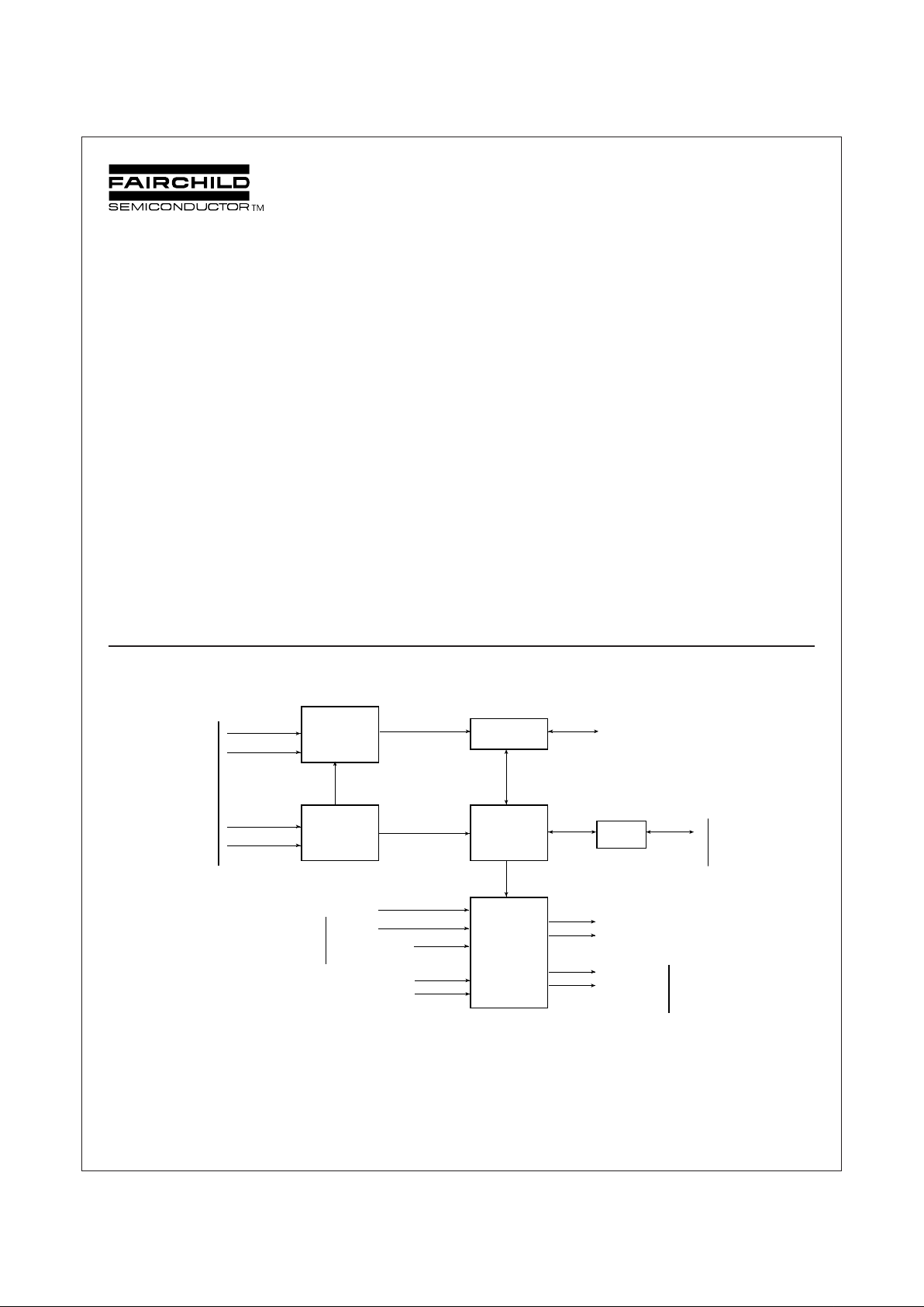
Block Diagram
Features
■ Complete Implementation of Plug and Play Standard
—Direct interface to ISA bus
■ Two modes of operation
—DMA mode
—Extended Interrupt mode (Windows® 95 logo
compatible)
■ 6 or 8 ISA bus interrupt lines and 2 DRQ/DACK lines
supported
■ On-chip EEPROM for resource request table
■ Additional 4 kbits of on-chip EEPROM available for external
access
■ 24 mA Drivers for Data outputs
■ Complete compliance to ISA PnP specification (Ver. 1.0A)
■ 48-Pin TQFP, and 52-Pin PLCC Packages
DS012601-1
Windows® 95 is a registered trademark of Microsoft Corporation.
Osc.
From
ISA
Bus
From
ISA
Bus
To
ISA
Bus
ISA
Bus
Rstdrv
Address
Control
Address
DACKx*
LIRQx
LDRQx
Control
IOCS<0:2>*
Function
Module
Support
Logic
State
Machine
Decoder
& Control
Register
Block
Data
Buffer
SD<0:7>
MICROWIRE Port
EEPROM
LDACKx*
IRQx
DRQx
Page 2
2
www.fairchildsemi.com
NM95MS16 Plug and Play Front-End Devices for ISA-BUS Systems
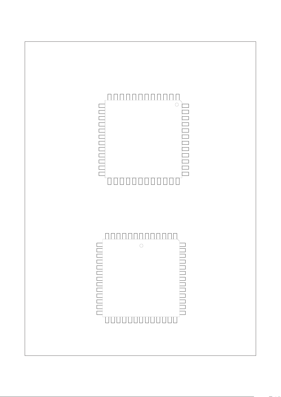
Connection Diagrams
Commercial Temperature Range (0°C to +70°C)
Order Number NM95MS16VBH
Order Number NM95MS16V
SA0
IRQOUT4
IRQOUT3
IRQOUT2
IRQOUT1
IRQOUT0
ISADRQ0/IRQOUT6
ISADRQ1/IRQOUT7
ISADACK0*/SA12
ISADACK1*/SA13
CS
SK
DI
SD7
SD6
SD5
SD4
SD2
SD1
SD0
OSC
AEN
DO
SD3
RSTDRV
IRQOUT5
IRQIN0
IRQIN1/SA14
GND
DRQIN/SA15
V
CC
IOWR*
IORD*
IOCS0*
IOCS1*
DACKOUT*/IOCS2*
SA11
SA1
SA2
SA3
SA4
SA5
SA6
SA7
SA8
SA9
SA10
GND
12 1234567891011
24
13
14
15
16
17
18
19
20
21
22
23
37
48
47
46
45
44
43
42
41
40
39
38
25 3635343332313029282726
NM95MS16
(TQFP)
1
23
45
6
7
12
9
10
11
13
14
15
16
17
18
19
20
36
48
46
45
44
43
42
41
40
39
38
37
24
22
23
25
33
32
313029
28
27
26
SA0
IRQOUT3
IRQOUT2
IRQOUT1
IRQOUT0
ISADRQ0/IRQOUT6
ISADRQ1/IRQOUT7
ISADACK0*/SA12
ISADACK1*/SA13
CS
SK
SD7
SD6
SD5
SD4
SD2
SD1
SD0
OSC
AEN
DO
SD3
IRQOUT5
IRQIN0
IRQIN1/SA14
GND
DRQIN/ISA15
VCC
IOWR*
IORD*
IOCS0*
IOCS1*
DACKOUT*/IOCS2*
SA11
SA2
SA3
SA4
SA5
SA6
SA7
SA8
SA9
SA10
GND
51
52 50 49
35
34
NC
NC
NC
47
21
8
NC
DI
IRQOUT4
RSTDRV
SA1
NM95MS16
(PLCC)
DS012601-2
DS012601-3
Page 3

3
www.fairchildsemi.com
NM95MS16 Plug and Play Front-End Devices for ISA-BUS Systems
Connection Diagrams (Continued)
Signals Type Description
SA<11:0> I Address inputs from the ISA bus.
IORD* I I/O read strobe from the ISA bus.
IOWR* I I/O write strobe from the ISA bus.
AEN I Address Enable from ISA Bus —used in conjunction with DMA.
SD<7:0> I/O Data bus —lower byte —from/to the ISA bus.
OSC (Note 1) I “OSC” clock from the ISA bus —used for internal state machines.
RSTDRV I Reset input from the ISA bus.
CS I Chip select for Microwire port. There should be a pull down
resistor of 4.7k on CS pin if unused externally, or directly
connected to GND.
SK, DI I Clock and Data input lines for Microwire bus connection to access
a portion (4k) on chip EEPROM.
DO O Data output line for the Microwire interface detailed above.
IRQOUT<5:0> O Connection to ISA bus interrupt request pins. On-chip interrupt
request(s) may be connected to any 6 of the ISA IRQ lines.
IRQIN<1:0> I Interrupt request from on-board logic
DRQin/SA<15> I DMA request from on-board logic, or Address input from ISA bus
depending on mode selected.
DACKOUT* /IOCS2* O DMA Acknowledge for on-board logic or Programmable chipselect
(2) depending on mode selected.
ISADRQ<1:0>/IRQOUT<7:6> O Connection for two ISA bus DMA Request lines, or additional
interrupt request lines depending on the mode selected.
ISADACK<1:0>*/SA<13:12> I DMA Acknowledge from the ISA bus or additional address lines
depending on the mode selected.
IOCS<1:0>* O Programmable chip selects to address on-board peripheral.
IRQIN<1>/SA<14> I Interrupt request from on board logic or Address input from ISA bus
depending on mode selected.
*Signal name with a “*” means its an active low signal.
Note 1: “OSC” clock from ISA Bus is fixed at a standard frequency of 14.318 MHz. NM95MS16 is designed and tested for 14.318 MHz. However NM95MS16 can handle
frequencies up to 24 MHz though it is not 100% tested.
Page 4
4
www.fairchildsemi.com
NM95MS16 Plug and Play Front-End Devices for ISA-BUS Systems
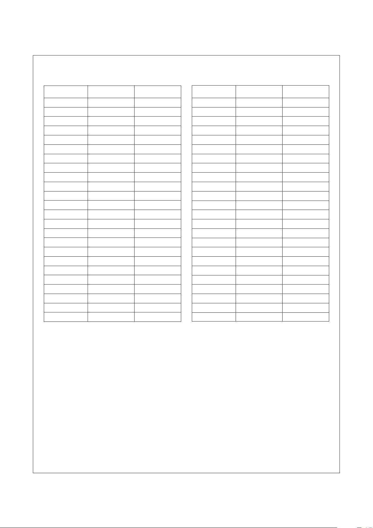
Pinout Details for the NM95MS16
Mode 00 = DMA Mode; Mode 01 = Extended Interrupt Mode
TQFP Pin DMA Mode Ext.Intr.Mode
1 RSTDRV RSTDRV
2 IOCS1* IOCS1*
3 IOCS0* IOCS0*
4 IORD* IORD*
5 IOWR* IOWR*
6VCCV
CC
7 DRQIN SA15
8 DACKOUT* IOCS2*
9 GND GND
10 IRQIN1 SA14
11 IRQIN0 IRQIN0
12 IRQOUT5 IRQOUT5
13 IRQOUT4 IRQOUT4
14 IRQOUT3 IRQOUT3
15 IRQOUT2 IRQOUT2
16 IRQOUT1 IRQOUT1
17 IRQOUT0 IRQOUT0
18 ISADRQ0 IRQOUT6
19 ISADRQ1 IRQOUT7
20 ISADACK0* SA12
21 ISADACK1* SA13
22 CS CS
23 SK SK
24 SA0 SA0
TQFP Pin DMA Mode Ext.Intr.Mode
25 SA1 SA1
26 SA2 SA2
27 SA3 SA3
28 SA4 SA4
29 GND GND
30 SA5 SA5
31 SA6 SA6
32 SA7 SA7
33 SA8 SA8
34 SA9 SA9
35 SA10 SA10
36 SA11 SA11
37 DI DI
38 DO DO
39 AEN AEN
40 OSC OSC
41 SD0 SD0
42 SD1 SD1
43 SD2 SD2
44 SD3 SD3
45 SD4 SD4
46 SD5 SD5
47 SD6 SD6
48 SD7 SD7
Note: Mode selection (00 or 01) is done by setting MS bits in the EEPROM configuration register. Detailed information about this is described in User’s Guide.
Page 5
5
www.fairchildsemi.com
NM95MS16 Plug and Play Front-End Devices for ISA-BUS Systems
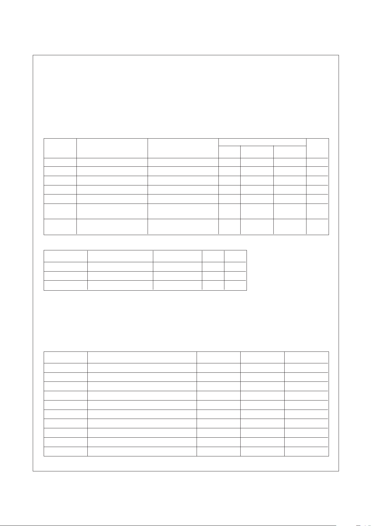
Absolute Maximum Ratings (Note 2)
Ambient Storage Temperature -65°C to +150°C
All Input or Output Voltages
with Respect to Ground VCC + 1V to -0.3V
Lead Temperature
(Soldering, 10 seconds) +300°C
ESD Rating 2000V Min
Operating Conditions
Ambient Operating Temperature
NM95MS16 0°C to +70°C
Positive Power Supply (VCC) 4.5V to 5.5V
DC Electrical Characteristics
Symbol Parameter Test Conditions Limits Units
Min Typ Max
(Note 3)
I
CCA
Active Power Supply Current f
SCL
= 100 kHz 15 mA
I
LI
Input Leakage Current VIN = GND or V
CC
0.2 15 µA
I
LO
Output Leakage Current V
OUT
= GND to V
CC
15 µA
V
IL
Input Low Voltage -0.1 0.8 V
V
IH
Input High Voltage 2.0 VCC + 1.0 V
V
OL
Output Low Voltage IOL = 24 mA (Note 5) 0.4 V
IOL = 2.1 mA (Note 6)
V
OH
Output High Voltage IOH = -3 mA (Note 5) 2.4 V
IOH = -400 µA (Note 6) 2.4 V
Capacitance T
A
= +25°C, f = 1.0 MHz, VCC = 5V
Symbol Test Conditions Max Units
CI/O (Note 4) Input/Output Capacitance VI/O = 0V 8 pF
CIN (Note 4) Input Capacitance VIN = 0V 6 pF
COUT (Note 4) Output Capacitance VOUT = 0V 6 pF
Note 2: Stress above those listed under "Absolute Maximum Ratings" may cause permanent damage to the device. This is a stress rating only, and functional operation of the
device at these or any other conditions above those indicated in the operational sections of the specification is not implied. Exposure to absolute maximum rating conditions for
extended periods may affect device reliability.
Note 3: Typical values are for TA = 25°C and nominal supply voltage (5V).
Note 4: This parameter is periodically sampled and not 100% tested.
Note 5: These values are for ISA signals like SD[0:7], IRQx, DRQx.
Note 6: These values are for card signal like IOCS[0:3]*, DO(EEPROM).
AC Electrical Characteristics
Symbol Parameter Min Max Unit
t
AEN
AEN Valid to Command Active 100 ns
t
AC
Address Valid to Command Active 88 ns
t
RVD
Active Read to Valid Data 200 ns
t
AH
Address, AEN Hold from Inactive Command 30 ns
t
RDH
Read Data Hold from Inactive Read 5 ns
t
WD
Write Data Valid before Write Active 22 ns
t
WDH
Write Data Hold after Write Inactive 25 ns
t
CSA
Chip Selects Valid from Address Valid 5 25 ns
t
CSC
Chip Selects Valid from Command Active 5 25 ns
t
IDD
Propagation Delay for IRQ/DRQ/DACK 5 25 ns
Page 6
6
www.fairchildsemi.com
NM95MS16 Plug and Play Front-End Devices for ISA-BUS Systems
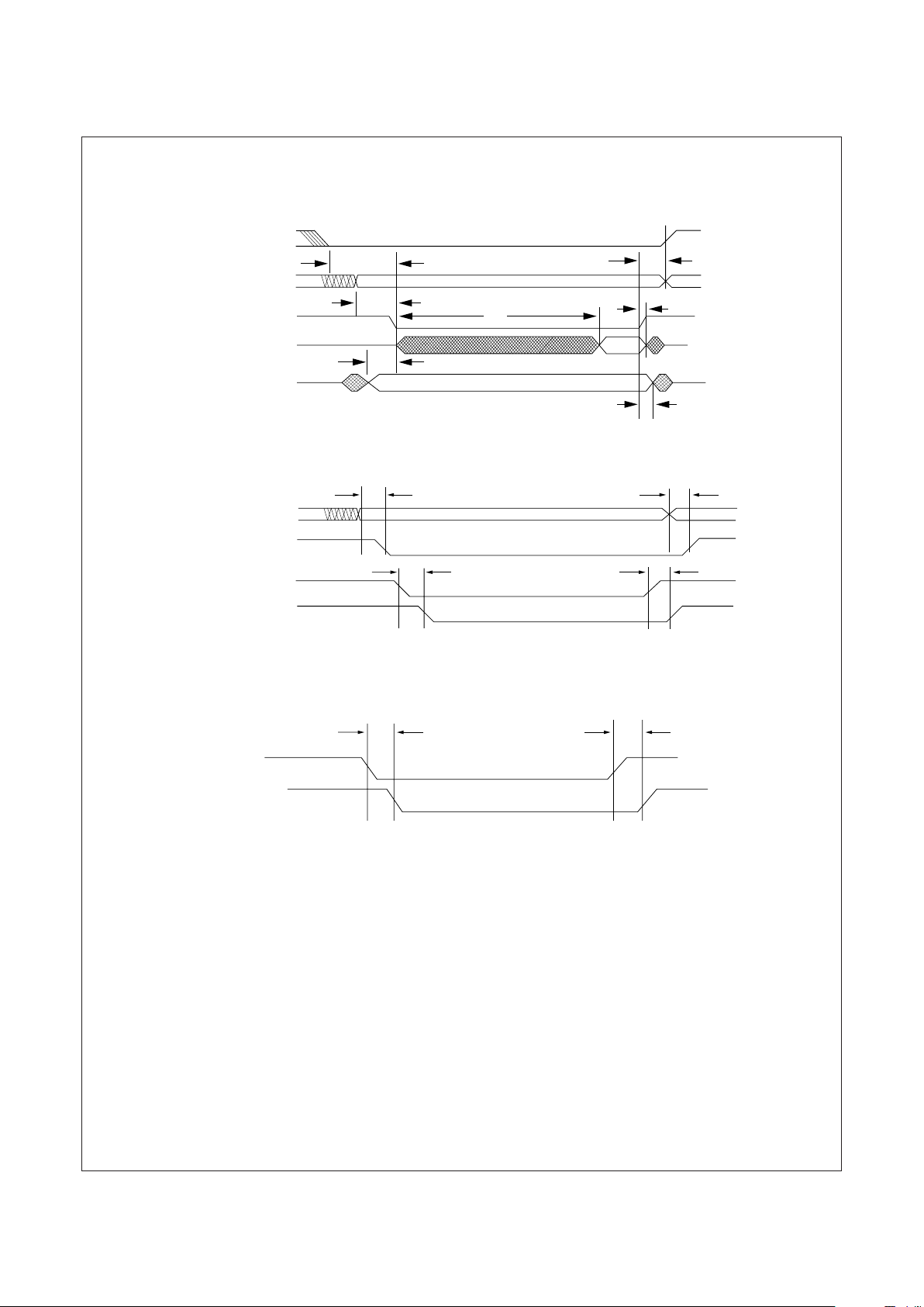
Timing Diagrams
Timings for ISA Read/Write Cycle
Decode Delay for Chipselect Generation
Propagation Delay for IRQ/DRQ/DACK
INTRODUCTION
The NM95MS16 is a single-chip solution for the ISA Plug and Play
(PnP) specification. It implements the complete state machine
and the necessary logic for supporting configurable Interrrupts
and DMA channels on the ISA bus for one logical device. Apart
from providing “PnP” capability, it has built-in EEPROM that
eliminates external EEPROM. This device is available in a space
saving 48-pin Thin Quad Flat Pack (TQFP) package.
Functional Description
NM95MS16 has two modes of operation, viz, “DMA mode” and
“Extended Interrupt mode”. These modes are programmed using
the mode select (MS) bits in one of the configuration registers
(Refer to the NM95MS16 User’s guide for detailed information).
Each of these modes are discussed below.
DMA Mode
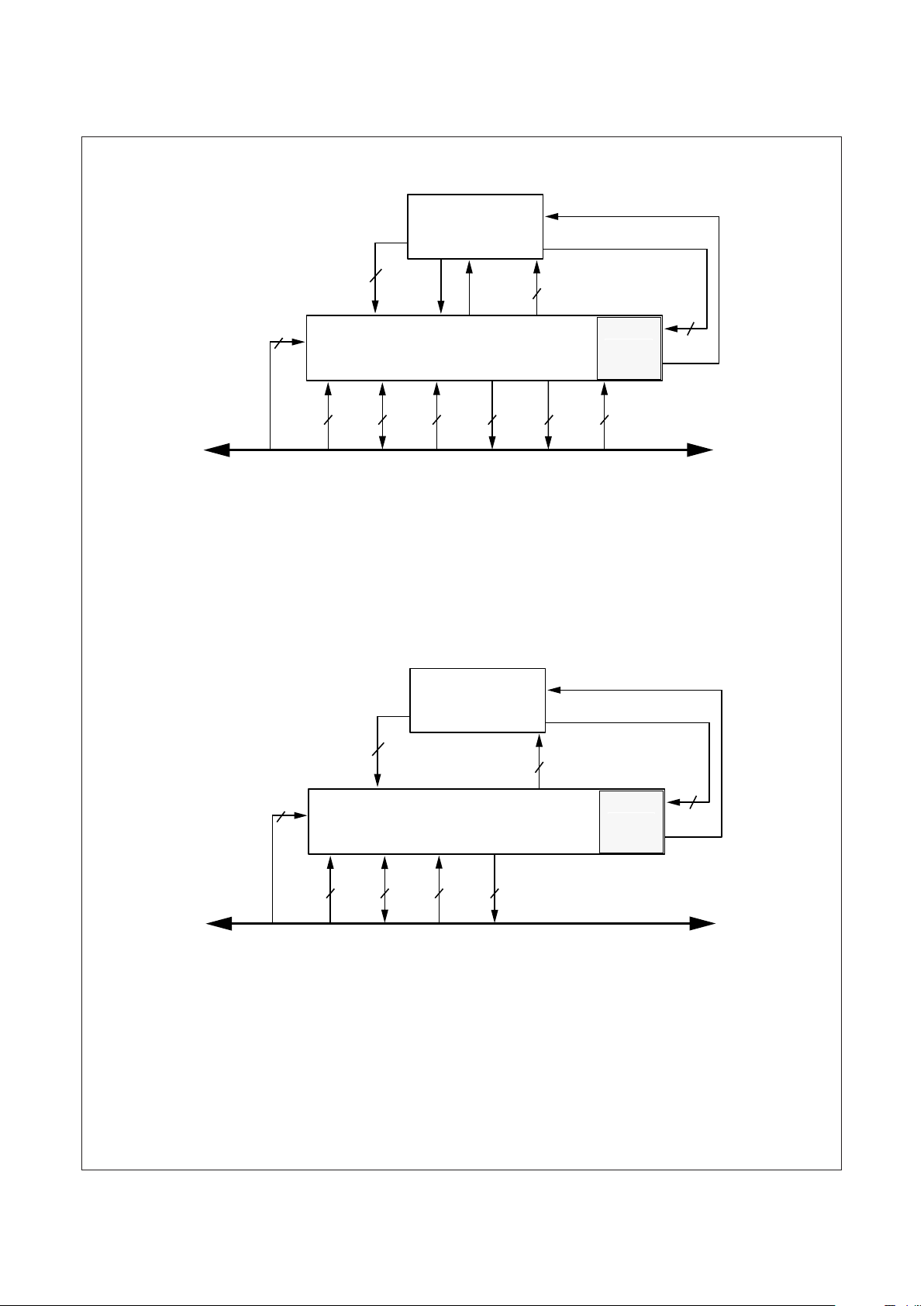
In the DMA mode, support is provided for
1. One on-board DMA request that is switchable to any two
DMA channels on the ISA bus.
2. Two on-board interrupt request lines switchable to any six
IRQ lines on the ISA bus.
3. Two programmable I/O chip selects for on-board logic.
Figure 1 shows a Block Diagram of NM95MS16 configured for
DMA Mode.
AEN
SA[0:11]
IORD*
IOWR*
READ DATA
SD[0:7]
t
RDH
WRITE DATA
SD[0:7]
t
AC
t
AH
VALID ADDRESS
VALID
t
WD
t
AEN
t
RVD
t
WDH
IORD*
IOWR*
t
CSC
t
CSC
IOCS[0:1]*
SA[0:11]
VALID ADDRESS
IOCS[0:1]*
t
CSA
t
CSA
(Qualified with CMD)
(addr decode only)
t
IDD
IRQin
DRQin
ISADACK
IRQout
DRQout
DACKout
t
IDD
DS012601-4
DS012601-5
DS012601-6
Page 7
7
www.fairchildsemi.com
NM95MS16 Plug and Play Front-End Devices for ISA-BUS Systems
INTRODUCTION (Continued)
FIGURE 1.
Extended Interrupt Mode
In the Ext.Int. mode, support is provided for:
1. Two on-board interrupt request lines switchable to any eight IRQ lines on the ISA bus.
2. Three programmable I/O chip selects for on-board logic.
3. ISA address SA12–SA15 are also included for extended decode.
Figure 2 shows a Block Diagram of NM95MS16 configured for Extended Interrupt Mode.
FIGURE 2.
Chipselect Generation
Individual I/O chipselect can be generated in the following two
ways:
A)Address Decode only
B)Address Decode qualified by Command (IORD*, IOWR*).
On-Chip EEPROM
NM95MS16 has 6 kbits of EEPROM on chip. All the PnP resource
data structure for the logical device is stored in this EEPROM. Of
the 6 kbits, 4 kbits are available for the logical device’s external
usage. The logical device can access the EEPROM through a
microwire port, which is essentially a 4-wire serial bus. The pins
CS, SK, DI and DO follow the exact timing as the standard
microwire bus and are compatible to the NM93Cxx family of
EEPROMs.
ISA BUS
SCSI/MODEM/ETHERNET
CONTROLLERS
NM95MS16
IOCS[0:1]DACKOUT*
DRQIN
CS,SK,DI
DO
IRQIN0
IRQIN1
FUNCTION MODULE
2
3
2
RSTDRV
OSC
2
IRQOUT
[0:5]
6
IORD*
IOWR*
AEN
3
SD[0:7]
8
SA[0:11]
DACK
[0:1]
2
DRQ
[0:1]
2
12
EEPROM
(DMA Mode)
ISA BUS
SERIAL I/O /MULTI-MEDIA
CONTROLLERS
NM95MS16
IOCS[0:2]
CS,SK,DI
DO
IRQIN0
FUNCTION MODULE
1
3
4
RSTDRV
OSC
2
IRQOUT
[0:7]
8
IORD*
IOWR*
AEN
3
SD[0:7]
8
SA[0:15]
16
EEPROM
(Extended Interrupt Mode)
DS012601-7
DS012601-8
Page 8
8
www.fairchildsemi.com
NM95MS16 Plug and Play Front-End Devices for ISA-BUS Systems
INTRODUCTION (Continued)
EEPROM Programming
The entire 6 kbits of EEPROM can be programmed through the
ISA bus. The EEPROM can be programmed by putting the device
(NM95MS16) in the Config. state (as defined in the PnP standard).
Under this state 4 registers at address 0xF0–0xF3 are accessible
to program the EEPROM. The data to be programmed is loaded
in register at address 0xF3 and 0xF2 (LSB and MSB respectively).
The address to be programmed is loaded in register at address
0xF1. The Ninth bit of address for 6 kbits of memory is provided
through the register at address 0xF0. Both read write are possible.
The actual operation does not begin until Go Ahead (GA) bit is set.
Programming a word takes approximately 10 ms. The status of the
operation can be polled by the Status bit. This bit is set when the
operation is in progress and will be reset when complete. The
register at address 0xF0 is COMMAND register. This is the
handshake register in programming the EEPROM and is explained below in a tabular format.
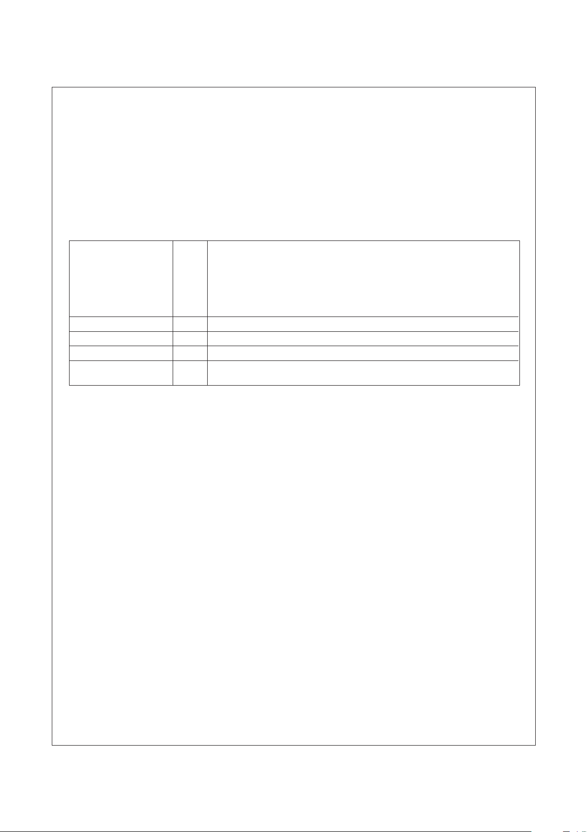
COMMAND Register 0xF0 Bit[1:0] —OP Code bits 10 - Read operation
01 - Write operation
11 - Erase operation
Bit[2] —GA(Go ahead bits)
If set to 1 the programming will continue.
Bit[6:3] —Reserved, should be 0.
Bit[7] —It provides A8 of the address. A[0:7] is provided by 0xF1 reg. (Note 7)
Address Register 0xF1 AddressRegister [A0–A7]
Data Register 0xF2 Data Byte [MSB]
Data Register 0xF3 Data Byte [LSB]
STATUS Register 0x05 Bit[0] —Status/Busy bit.
“0” if busy, “1” is done.
Note 7: The PNP resource data portion of the internal memory is at high address. Hence to program that portion, bit [7] of register 0xF0 (Address A8) should be set to “1”.
Page 9
9
www.fairchildsemi.com
NM95MS16 Plug and Play Front-End Devices for ISA-BUS Systems
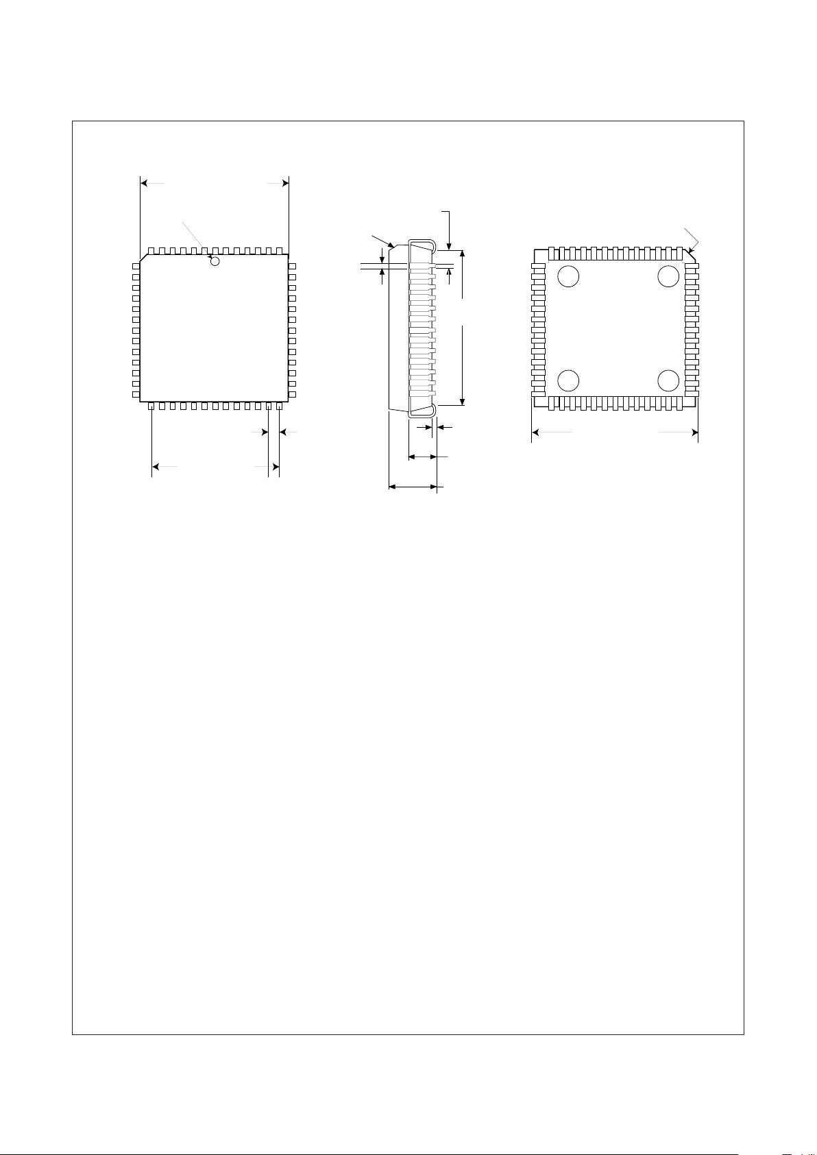
52-Lead Molded Plastic Leaded Chip Carrier
Package Number V52A
Order Number NM95MS16V
Physical Dimensions inches (millimeters) unless otherwise noted
45° X
0.045
[1.14]
0.785 - 0.795
[19.94 - 20.19]
0.600
[15.24]
TYP
0.050
[1.27]
TYP
17
8
20
21 33
34
46
52
Pin 1 IDENT
47
0.750 - 0.756
[19.05 - 19.20]
0.026–0.032
[0.66–0.81]
0.013–0.021
[0.33–0.53]
0.045
[1.14]
0.020
[0.51]
0.690–0.730
[17.53–18.54]
0.090–0.130
[2.29–3.30]
TYP
TYP
MIN TYP
TYP
0.165–0.180
[4.19–4.57]
TYP
TYP
45°X
Page 10
10
www.fairchildsemi.com
NM95MS16 Plug and Play Front-End Devices for ISA-BUS Systems
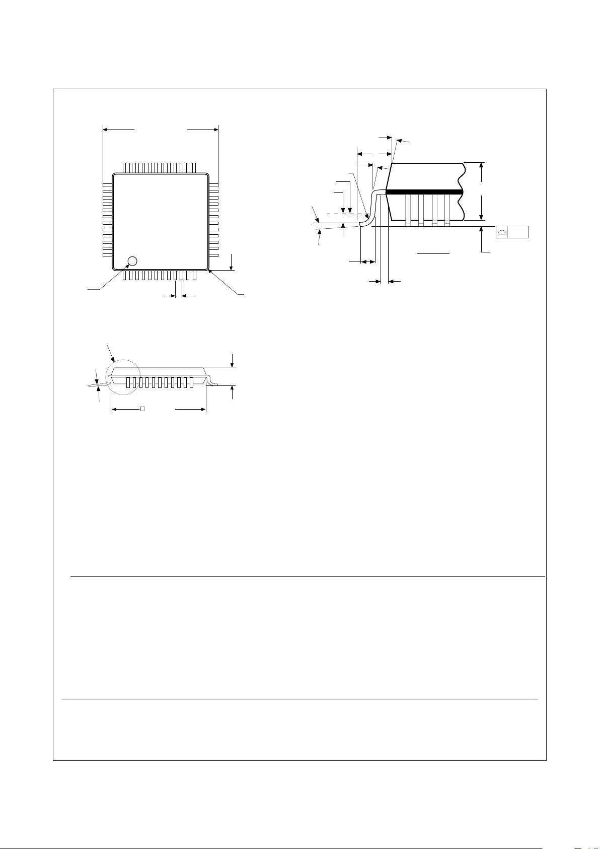
Physical Dimensions inches (millimeters) unless otherwise noted
TQFP Package (VBH)
Package Number VBH48A
Order Number NM95MS16VBH
1.40 ±0.05
1.6 MAX
0.08
Seating
Plane
0.20 Min
0.05 - 0.10
12° Top and Bottom
0° Min
Gage plane
R 0.08 – 0.20
0.25
DETAIL A
Typical
See Detail A
9.0
± 0.25 Typ
1.0
112
36 25
13
Pin #1
Ident
24
48
37
0.5 Typ.
7.0 ±0.1
0.60
±0.15
0°- 7°
0.125 Typ
Optional:
Sharp corners
except Pin #1
Ident corner
Fairchild does not assume any responsibility for use of any circuitry described, no circuit patent licenses are implied and Fairchild reserves the right at any time without notice to change said circuitry and specifications.
Life Support Policy
Fairchild's products are not authorized for use as critical components in life support devices or systems without the express written
approval of the President of Fairchild Semiconductor Corporation. As used herein:
1. Life support devices or systems are devices or systems which,
(a) are intended for surgical implant into the body, or (b) support
or sustain life, and whose failure to perform, when properly
used in accordance with instructions for use provided in the
labeling, can be reasonably expected to result in a significant
injury to the user.
2. A critical component is any component of a life support device
or system whose failure to perform can be reasonably expected to cause the failure of the life support device or system,
or to affect its safety or effectiveness.
Fairchild Semiconductor Fairchild Semiconductor Fairchild Semiconductor Fairchild Semiconductor
Americas Europe Hong Kong Japan Ltd.
Customer Response Center Fax: +44 (0) 1793-856858 8/F, Room 808, Empire Centre 4F, Natsume Bldg.
Tel. 1-888-522-5372 Deutsch Tel: +49 (0) 8141-6102-0 68 Mody Road, Tsimshatsui East 2-18-6, Yushima, Bunkyo-ku
English Tel: +44 (0) 1793-856856 Kowloon. Hong Kong Tokyo, 113-0034 Japan
Français Tel: +33 (0) 1-6930-3696 Tel; +852-2722-8338 Tel: 81-3-3818-8840
Italiano Tel: +39 (0) 2-249111-1 Fax: +852-2722-8383 Fax: 81-3-3818-8841
 Loading...