

Page 1
February 2000
NM93CS56
(MICROWIRE™ Bus Interface) 2048-Bit Serial EEPROM
with Data Protect and Sequential Read
with Data Protect and Sequential Read
NM93CS56 (MICROWIRE Bus Interface) 2048-Bit Serial EEPROM
General Description
NM93CS56 is a 2048-bit CMOS non-volatile EEPROM organized
as 128 x 16-bit array. This device features MICROWIRE interface
which is a 4-wire serial bus with chipselect (CS), clock (SK), data
input (DI) and data output (DO) signals. This interface is compatible to many of standard Microcontrollers and Microprocessors.
NM93CS56 offers programmable write protection to the memory
array using a special register called Protect Register. Selected
memory locations can be protected against write by programming
this Protect Register with the address of the first memory location
to be protected (all locations greater than or equal to this first
address are then protected from further change). Additionally, this
address can be “permanently locked” into the device, making all
future attempts to change data impossible. In addition this device
features “sequential read”, by which, entire memory can be read
in one cycle instead of multiple single byte read cycles. There are
10 instructions implemented on the NM93CS56, 5 of which are for
memory operations and the remaining 5 are for Protect Register
operations. This device is fabricated using Fairchild Semiconductor floating-gate CMOS process for high reliability, high endurance
and low power consumption.
“LZ” and “L” versions of NM93CS56 offer very low standby current
making them suitable for low power applications. This device is offered
in both SO and TSSOP packages for small space considerations.
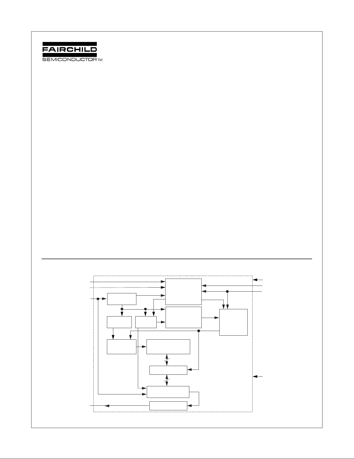
Functional Diagram
CS
SK
DI
INSTRUCTION
REGISTER
Features
■ Wide VCC 2.7V - 5.5V
■ Programmable write protection
■ Sequential register read
■ Typical active current of 200µA
10µA standby current typical
1µA standby current typical (L)
0.1µA standby current typical (LZ)
■ No Erase instruction required before Write instruction
■ Self timed write cycle
■ Device status during programming cycles
■ 40 year data retention
■ Endurance: 1,000,000 data changes
■ Packages available: 8-pin SO, 8-pin DIP, 8-pin TSSOP
V
INSTRUCTION
DECODER
CONTROL LOGIC
AND CLOCK
GENERATORS
CC
PRE
PE
DO
© 1999 Fairchild Semiconductor Corporation
NM93CS56 Rev. F.2
ADDRESS
REGISTER
DECODER
PROTECT
REGISTER
EEPROM ARRAY
READ/WRITE AMPS
DATA IN/OUT REGISTER
DATA OUT BUFFER
COMPARATOR
WRITE ENABLE
16
16
16 BITS
AND
1
HIGH VOLTAGE
GENERATOR
AND
PROGRAM
TIMER
V
SS
www.fairchildsemi.com
Page 2
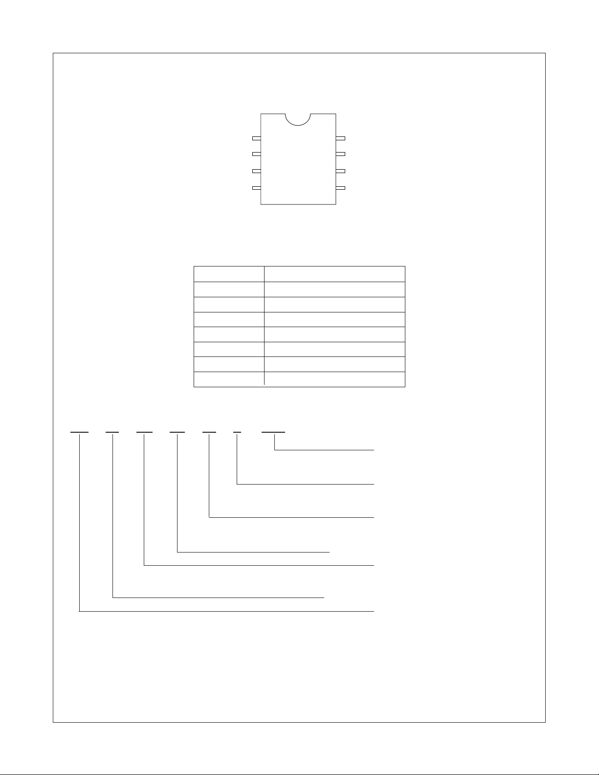
Connection Diagram
Dual-In-Line Package (N)
8–Pin SO (M8) and 8–Pin TSSOP (MT8)
with Data Protect and Sequential Read
NM93CS56 (MICROWIRE Bus Interface) 2048-Bit Serial EEPROM
Pin Names
Ordering Information
CS
SK
DI
DO
1
2
3
4
8
V
CC
7
PRE
6
PE
5
GND
Top View
Package Number
N08E, M08A and MTC08
CS Chip Select
SK Serial Data Clock
DI Serial Data Input
DO Serial Data Output
GND Ground
PE Program Enable
PRE Protect Register Enable
V
CC
Power Supply
NM 93 CS XX LZ E XXX Letter Description
Package N 8-pin DIP
M8 8-pin SO
MT8 8-pin TSSOP
Temp. Range None 0 to 70°C
V -40 to +125°C
E -40 to +85°C
Voltage Operating Range Blank 4.5V to 5.5V
L 2.7V to 5.5V
LZ 2.7V to 5.5V and
Density 56 2048 bits
C CMOS
CS Data protect and sequential
Interface 93 MICROWIRE
Fairchild Memory Prefix
<1µA Standby Current
read
NM93CS56 Rev. F.2
2
www.fairchildsemi.com
Page 3
with Data Protect and Sequential Read
NM93CS56 (MICROWIRE Bus Interface) 2048-Bit Serial EEPROM
Absolute Maximum Ratings (Note 1)
Ambient Storage Temperature -65°C to +150°C
All Input or Output Voltages +6.5V to -0.3V
with Respect to Ground
Lead Temperature
(Soldering, 10 sec.) +300°C
Operating Conditions
Ambient Operating Temperature
NM93CS56 0°C to +70°C
NM93CS56E -40°C to +85°C
NM93CS56V -40°C to +125°C
Power Supply (V
) 4.5V to 5.5V
CC
ESD rating 2000V
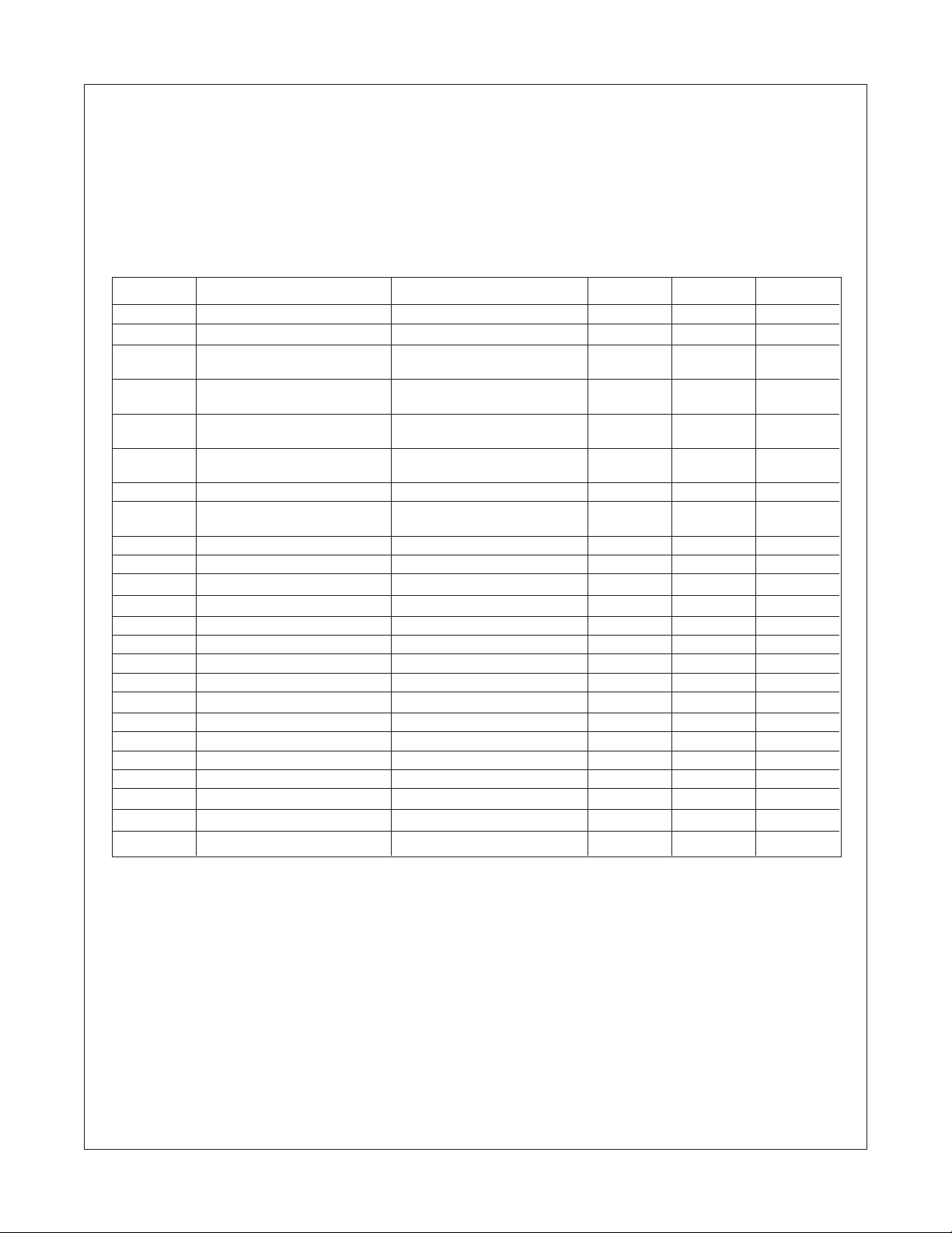
DC and AC Electrical Characteristics V
= 4.5V to 5.5V unless otherwise specified
CC
Symbol Parameter Conditions Min Max Units
I
CCA
I
CCS
I
V
V
V
V
V
V
f
t
SKH
t
SKL
t
SKS
t
t
CSS
t
PRES
t
t
PES
t
t
CSH
t
PEH
t
PREH
t
t
t
t
t
I
IL
OL
OL1
OH1
OL2
OH2
SK
CS
DH
DIS
DIH
PD
SV
DF
WP
IL
IH
Operating Current CS = VIH, SK=1.0 MHz 1 mA
Standby Current CS = V
IL
Input Leakage VIN = 0V to V
Output Leakage (Note 2)
CC
50 µA
±-1 µA
Input Low Voltage -0.1 0.8 V
Input High Voltage 2 VCC +1
Output Low Voltage IOL = 2.1 mA 0.4 V
Output High Voltage IOH = -400 µA 2.4
Output Low Voltage IOL = 10 µA 0.2 V
Output High Voltage IOH = -10 µAV
CC
- 0.2
SK Clock Frequency (Note 3) 1 MHz
SK High Time 0°C to +70°C 250 ns
-40°C to +125°C 300
SK Low Time 250 ns
SK Setup Time 50 ns
Minimum CS Low Time (Note 4) 250 ns
CS Setup Time 100 ns
PRE Setup Time 50 ns
DO Hold Time 70 ns
PE Setup Time 50 ns
DI Setup Time 100 ns
CS Hold Time 0 ns
PE Hold Time 250 ns
PRE Hold Time 50 ns
DI Hold Time 20 ns
Output Delay 500 ns
CS to Status Valid 500 ns
CS to DO in Hi-Z CS = V
IL
100 ns
Write Cycle Time 10 ms
NM93CS56 Rev. F.2
3
www.fairchildsemi.com
Page 4
with Data Protect and Sequential Read
NM93CS56 (MICROWIRE Bus Interface) 2048-Bit Serial EEPROM
Absolute Maximum Ratings (Note 1)
Ambient Storage Temperature -65°C to +150°C
All Input or Output Voltages +6.5V to -0.3V
with Respect to Ground
Lead Temperature
(Soldering, 10 sec.) +300°C
Operating Conditions
Ambient Operating Temperature
NM93CS56L/LZ 0°C to +70°C
NM93CS56LE/LZE -40°C to +85°C
NM93CS56LV/LZV -40°C to +125°C
Power Supply (V
) 2.7V to 5.5V
CC
ESD rating 2000V
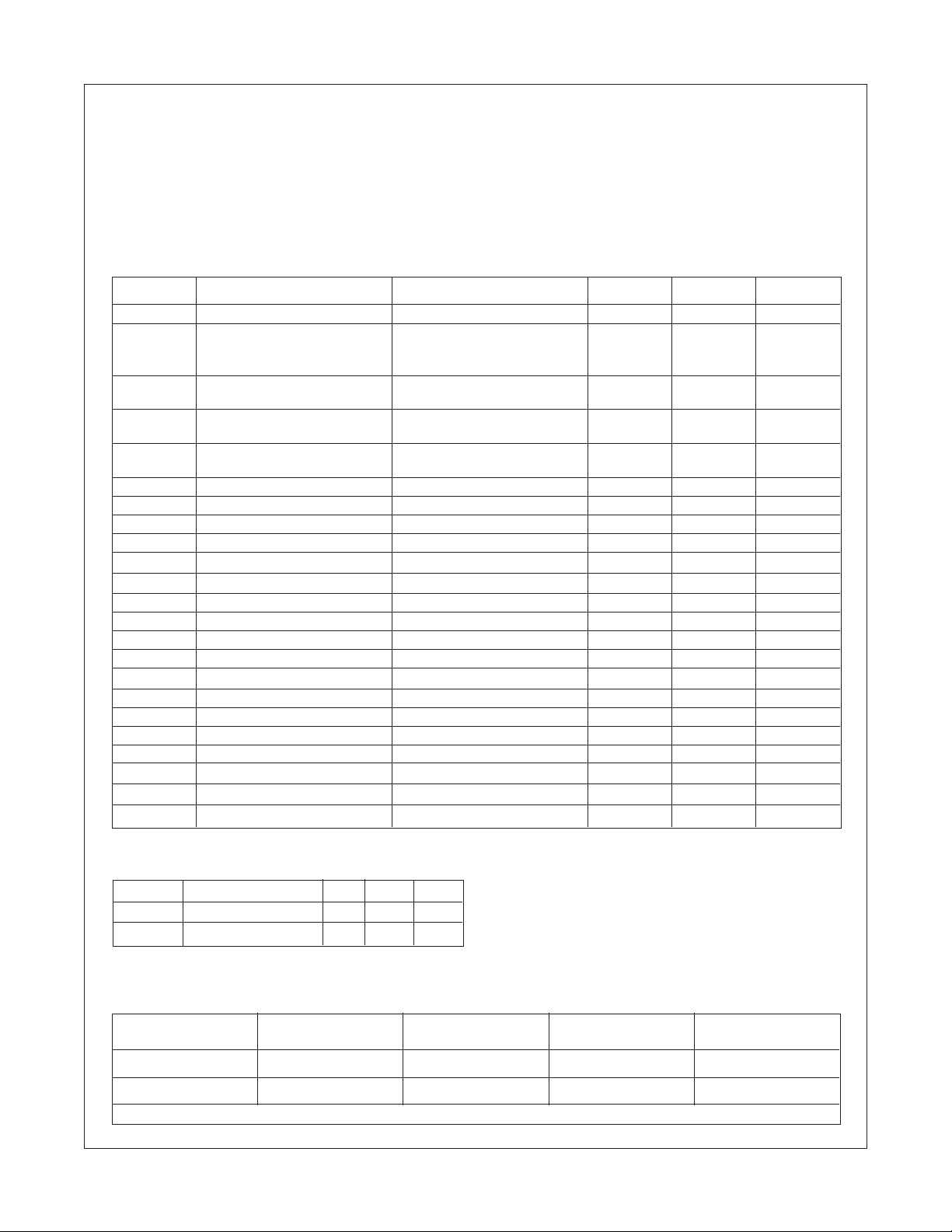
DC and AC Electrical Characteristics V
= 2.7V to 5.5V unless otherwise specified
CC
Symbol Parameter Conditions Min Max Units
I
CCA
I
CCS
I
IL
I
OL
V
IL
V
IH
V
OL
V
OH
f
SK
t
SKH
t
SKL
t
SKS
t
CS
t
CSS
t
PRES
t
DH
t
PES
t
DIS
t
CSH
t
PEH
t
PREH
t
DIH
t
PD
t
SV
t
DF
t
WP
Capacitance TA = 25°C, f = 1 MHz (Note 5)
Symbol Test Typ Max Units
C
OUT
C
IN
Operating Current CS = VIH, SK=1.0 MHz 1 mA
Standby Current CS = V
L 10 µA
IL
LZ (2.7V to 4.5V) 1 µA
Input Leakage VIN = 0V to V
CC
±1 µA
Output Leakage (Note 2)
Input Low Voltage -0.1 0.15V
Input High Voltage 0.8V
CC
Output Low Voltage IOL = 10µA 0.1V
Output High Voltage IOH = -10µA 0.9V
CC
CC
VCC +1
CC
SK Clock Frequency (Note 3) 0 250 KHz
SK High Time 1 µs
SK Low Time 1 µs
SK Setup Time 0.2 µs
Minimum CS Low Time (Note 4) 1 µs
CS Setup Time 0.2 µs
PRE Setup Time 50 ns
DO Hold Time 70 ns
PE Setup Time 50 ns
DI Setup Time 0.4 µs
CS Hold Time 0 ns
PE Hold Time 250 ns
PRE Hold Time 50 ns
DI Hold Time 0.4 µs
Output Delay 2 µs
CS to Status Valid 1 µs
CS to DO in Hi-Z CS = V
IL
0.4 µs
Write Cycle Time 15 ms
Note 1: Stress above those listed under “Absolute Maximum Ratings” may cause permanent damage
to the device. This is a stress rating only and functional operation of the device at these or any other
conditions above those indicated in the operational sections of the specification is not implied. Exposure
to absolute maximum rating conditions for extended periods may affect device reliability.
Output Capacitance 5 pF
Input Capacitance 5 pF
Note 2: Typical leakage values are in the 20nA range.
Note 3: The shortest allowable SK clock period = 1/f
SK clock speed (minimum SK period) is determined by the interaction of several AC parameters stated
in the datasheet. Within this SK period, both t
allowable to set 1/fSK = t
Note 4: CS (Chip Select) must be brought low (to V
device registers (device reset) prior to beginning another opcode cycle. (This is shown in the opcode
diagram on the following page.)
Note 5: This parameter is periodically sampled and not 100% tested.
SKHminimum
+ t
SKLminimum
(as shown under the fSK parameter). Maximum
SK
and t
limits must be observed. Therefore, it is not
SKH
SKL
for shorter SK cycle time operation.
) for an interval of tCS in order to reset all internal
IL
AC Test Conditions
VCC Range VIL/V
Input Levels Timing Level Timing Level
IH
2.7V ≤ VCC ≤ 5.5V 0.3V/1.8V 1.0V 0.8V/1.5V ±10µA
(Extended Voltage Levels)
4.5V ≤ VCC ≤ 5.5V 0.4V/2.4V 1.0V/2.0V 0.4V/2.4V 2.1mA/-0.4mA
(TTL Levels)
Output Load: 1 TTL Gate (CL = 100 pF)
VIL/V
IH
VOL/V
OH
IOL/I
OH
V
V
NM93CS56 Rev. F.2
4
www.fairchildsemi.com
Page 5
with Data Protect and Sequential Read
NM93CS56 (MICROWIRE Bus Interface) 2048-Bit Serial EEPROM
Pin Description
Chip Select (CS)
This is an active high input pin to NM93CS56 EEPROM (the device)
and is generated by a master that is controlling the device. A high
level on this pin selects the device and a low level deselects the
device. All serial communications with the device is enabled only
when this pin is held high. However this pin cannot be permanently
tied high, as a rising edge on this signal is required to reset the
internal state-machine to accept a new cycle and a falling edge to
initiate an internal programming after a write cycle. All activity on the
SK, DI and DO pins are ignored while CS is held low.
Serial Clock (SK)
This is an input pin to the device and is generated by the master that
is controlling the device. This is a clock signal that synchronizes the
communication between a master and the device. All input information (DI) to the device is latched on the rising edge of this clock input,
while output data (DO) from the device is driven from the rising edge
of this clock input. This pin is gated by CS signal.
Serial Input (DI)
This is an input pin to the device and is generated by the master
that is controlling the device. The master transfers Input information (Start bit, Opcode bits, Array addresses and Data) serially via
this pin into the device. This Input information is latched on the
rising edge of the SCK. This pin is gated by CS signal.
Serial Output (DO)
This is an output pin from the device and is used to transfer Output
data via this pin to the controlling master. Output data is serially
shifted out on this pin from the rising edge of the SCK. This pin is
active only when the device is selected.
Protect Register Enable (PRE)
This is an active high input pin to the device and is used to
distinguish operations to memory array and operations to Protect
Register. When this pin is held low, operations to the memory
array are enabled. When this pin is held high, operations to the
Protect Register are enabled. This pin operates in conjunction
with PE pin. Refer Table1 for functional matrix of this pin for
various operations.
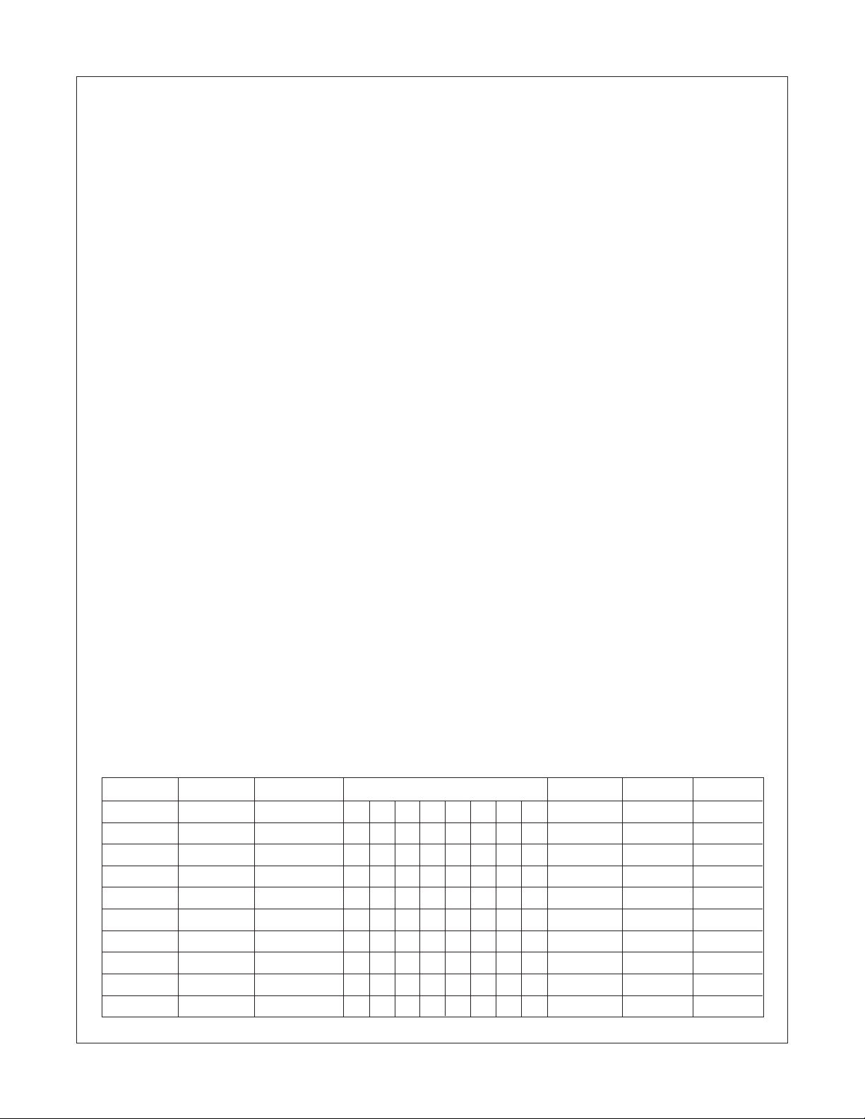
TABLE 1. Instruction set
Program Enable (PE)
This is an active high input pin to the device and is used to enable
operations, that are write in nature, to the memory array and to the
Protect register. When this pin is held high, operations that are
“write” in nature are enabled. When this pin is held low, operations
that are “write” in nature are disabled. This pin operates in
conjunction with PRE pin. Refer Table1 for functional matrix of this
pin for various operations.
Microwire Interface
A typical communication on the Microwire bus is made through the
CS, SK, DI and DO signals. To facilitate various operations on the
Memory array and on the Protect Register, a set of 10 instructions
are implemented on NM93CS56. The format of each instruction is
listed in Table 1.
Instruction
Each of the above 10 instructions is explained under individual
instruction descriptions.
Start Bit
This is a 1-bit field and is the first bit that is clocked into the device
when a Microwire cycle starts. This bit has to be “1” for a valid cycle
to begin. Any number of preceding “0” can be clocked into the
device before clocking a “1”.
Opcode
This is a 2-bit field and should immediately follow the start bit.
These two bits (along with PRE, PE signals and 2 MSB of address
field) select a particular instruction to be executed.
Address Field
This is a 8-bit field and should immediately follow the Opcode bits.
In NM93CS56, only the LSB 7 bits are used for address decoding
during READ, WRITE and PRWRITE instructions. During these
three instructions (READ, WRITE and PRWRITE), the MSB is
“don’t care” (can be 0 or 1). During all other instructions (with the
exception of PRREAD), the MSB 2 bits are used to decode
instruction (along with Opcode bits, PRE and PE signals).
Data Field
This is a 16-bit field and should immediately follow the Address
bits. Only the WRITE and WRALL instructions require this field.
D15 (MSB) is clocked first and D0 (LSB) is clocked last (both
during writes as well as reads).
Instruction Start Bit Opcode Field Address Field Data Field PRE Pin PE Pin
READ 1 10 X A6 A5 A4 A3 A2 A1 A0 0 X
WEN 1 00 11XXXXXX 0 1
WRITE 1 01 X A6 A5 A4 A3 A2 A1 A0 D15-D0 0 1
WRALL 1 00 0 1 X X XXXX D15-D0 0 1
WDS 1 00 0 0XXXXXX 0 X
PRREAD 1 10 XXXXXXXX 1 X
PREN 1 00 1 1 X X XXXX 1 1
PRCLEAR 1 11 11111111 1 1
PRWRITE 1 01 X A6 A5 A4 A3 A2 A1 A0 1 1
PRDS 1 00 00000000 1 1
5
NM93CS56 Rev. F.2
www.fairchildsemi.com
Page 6

with Data Protect and Sequential Read
NM93CS56 (MICROWIRE Bus Interface) 2048-Bit Serial EEPROM
Functional Description
A typical Microwire cycle starts by first selecting the device
(bringing the CS signal high). Once the device is selected, a valid
Start bit (“1”) should be issued to properly recognize the cycle.
Following this, the 2-bit opcode of appropriate instruction should
be issued. After the opcode bits, the 8-bit address information
should be issued. For certain instructions, some (or all) of these
8 bits are don’t care values (can be “0” or “1”), but they should still
be issued. Following the address information, depending on the
instruction (WRITE and WRALL), 16-Bit data is issued. Otherwise, depending on the instruction (READ and PRREAD), the
device starts to drive the output data on the DO line. Other
instructions perform certain control functions and do not deal with
data bits. The Microwire cycle ends when the CS signal is brought
low. However during certain instructions, falling edge of the CS
signal initiates an internal cycle (Programming), and the device
remains busy till the completion of the internal cycle. Each of the
10 instructions is explained in detail in the following sections.
Memory Instructions
Following five instructions, READ, WEN, WRITE, WRALL and
WDS are specific to operations intended for memory array. The
PRE pin should be held low during these instructions.
1) Read and Sequential Read (READ)
READ instruction allows data to be read from a selected location
in the memory array. Input information (Start bit, Opcode and
Address) for this instruction should be issued as listed under
Table1. Upon receiving a valid input information, decoding of the
opcode and the address is made, followed by data transfer from
the selected memory location into a 16-bit serial-out shift register.
This 16-bit data is then shifted out on the DO pin. D15 bit (MSB)
is shifted out first and D0 bit (LSB) is shifted out last. A dummy-bit
(logical 0) precedes this 16-bit data output string. Output data
changes are initiated on the rising edge of the SK clock. After
reading the 16-bit data, the CS signal can be brought low to end
the Read cycle. The PRE pin should be held low during this cycle.
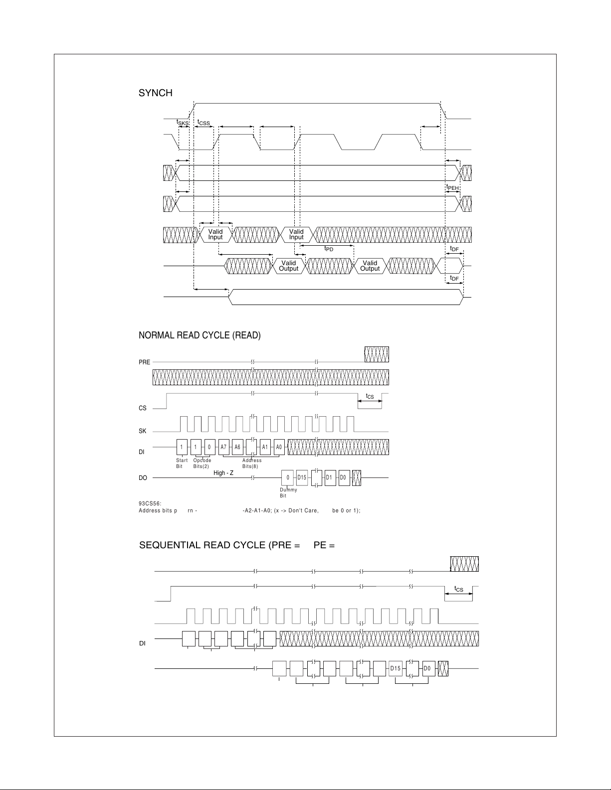
Refer
Read cycle diagram
This device also offers “sequential memory read” operation to
allow reading of data from the additional memory locations instead
of just one location. It is started in the same manner as normal read
but the cycle is continued to read further data (instead of terminating after reading the first 16-bit data). After providing 16-bit data,
the device automatically increments the address pointer to the
next location and continues to provide the data from that location.
Any number of locations can be read out in this manner, however,
after reading out from the last location, the address pointer points
back to the first location. If the cycle is continued further, data will
be read from this first location onward. In this mode of read, the
dummy-bit is present only when the very first data is read (like
normal read cycle) and is not present on subsequent data reads.
The PRE pin should be held low during this cycle. Refer
tial Read cycle diagram
2) Write Enable (WEN)
When VCC is applied to the part, it “powers up” in the Write Disable
(WDS) state. Therefore, all programming operations (for both
memory array and Protect Register) must be preceded by a Write
Enable (WEN) instruction. Once a Write Enable instruction is
executed, programming remains enabled until a Write Disable
(WDS) instruction is executed or VCC is completely removed from
.
Sequen-
.
the part. Input information (Start bit, Opcode and Address) for this
WEN instruction should be issued as listed under Table1. The
device becomes write-enabled at the end of this cycle when the
CS signal is brought low. The PRE pin should be held low during
this cycle. Execution of a READ instruction is independent of WEN
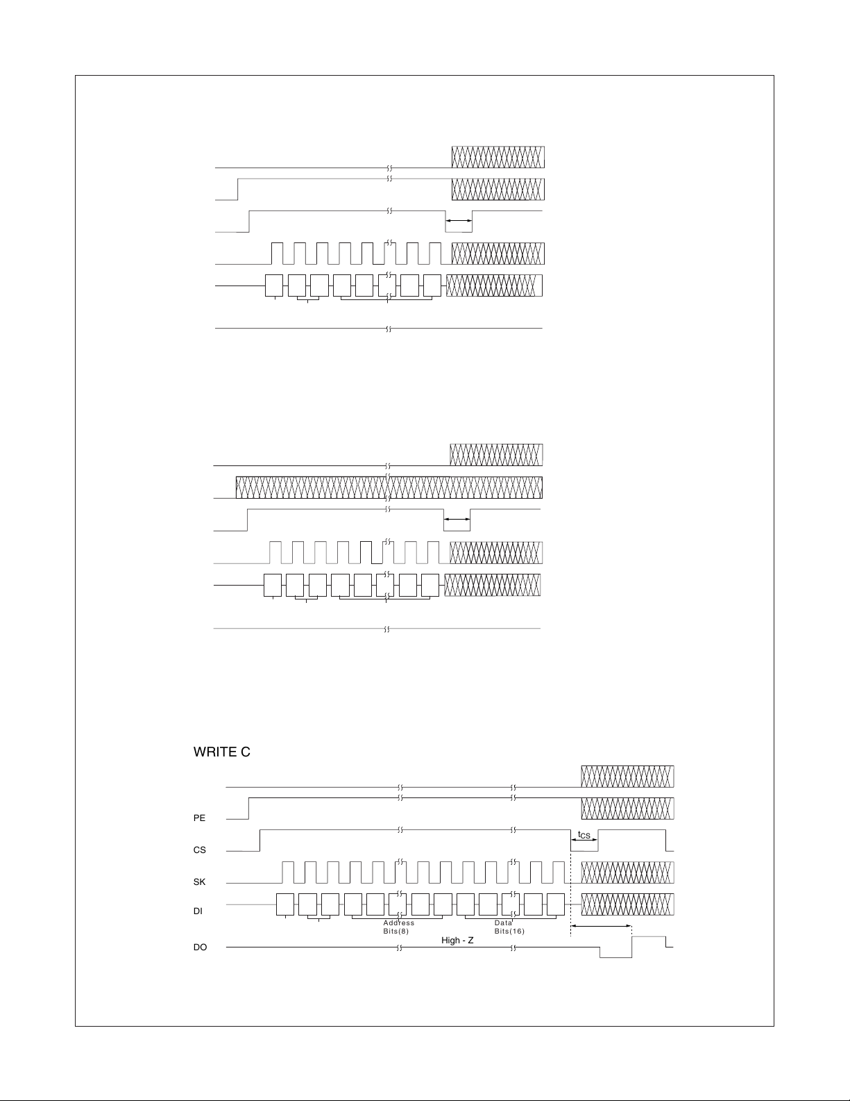
instruction. Refer
Write Enable cycle diagram.
3) Write (WRITE)
WRITE instruction allows write operation to a specified location in
the memory with a specified data. This instruction is valid only
when the following are true:
■ Device is write-enabled (Refer WEN instruction)
■ Address of the write location is not write-protected
■ PE pin is held high during this cycle
■ PRE pin should be held low during this cycle
Input information (Start bit, Opcode, Address and Data) for this
WRITE instruction should be issued as listed under Table1. After
inputting the last bit of data (D0 bit), CS signal must be brought low
before the next rising edge of the SK clock. This falling edge of the
CS initiates the self-timed programming cycle. It takes t
(Refer appropriate DC and AC Electrical Characteristics table) for
the internal programming cycle to finish. During this time, the
device remains busy and is not ready for another instruction.
The status of the internal programming cycle can be polled at any
time by bringing the CS signal high again, after tCS interval. When
CS signal is high, the DO pin indicates the READY/BUSY status
of the chip. DO = logical 0 indicates that the programming is still
in progress. DO = logical 1 indicates that the programming is
finished and the device is ready for another instruction. It is not
required to provide the SK clock during this status polling. While
the device is busy, it is recommended that no new instruction be
issued. Refer
It is also recommended to follow this instruction (after the device
becomes READY) with a Write Disable (WDS) instruction to
safeguard data against corruption due to spurious noise, inadvertent writes etc.
Write cycle diagram.
WP
time
4) Write All (WRALL)
Write all (WRALL) instruction is similar to the Write instruction
except that WRALL instruction will simultaneously program all
memory locations with the data pattern specified in the instruction.
This instruction is valid only when the following are true:
■ Protect Register has been cleared (Refer PRCLEAR
instruction)
■ Device is write-enabled (Refer WEN instruction)
■ PE pin is held high during this cycle
■ PRE pin should be held low during this cycle
Input information (Start bit, Opcode, Address and Data) for this
WRALL instruction should be issued as listed under Table1. After
inputting the last bit of data (D0 bit), CS signal must be brought low
before the next rising edge of the SK clock. This falling edge of the
CS initiates the self-timed programming cycle. It takes tWP time
(Refer appropriate DC and AC Electrical Characteristics table) for
the internal programming cycle to finish. During this time, the
device remains busy and is not ready for another instruction.
Status of the internal programming can be polled as described
under WRITE instruction description. While the device is busy, it
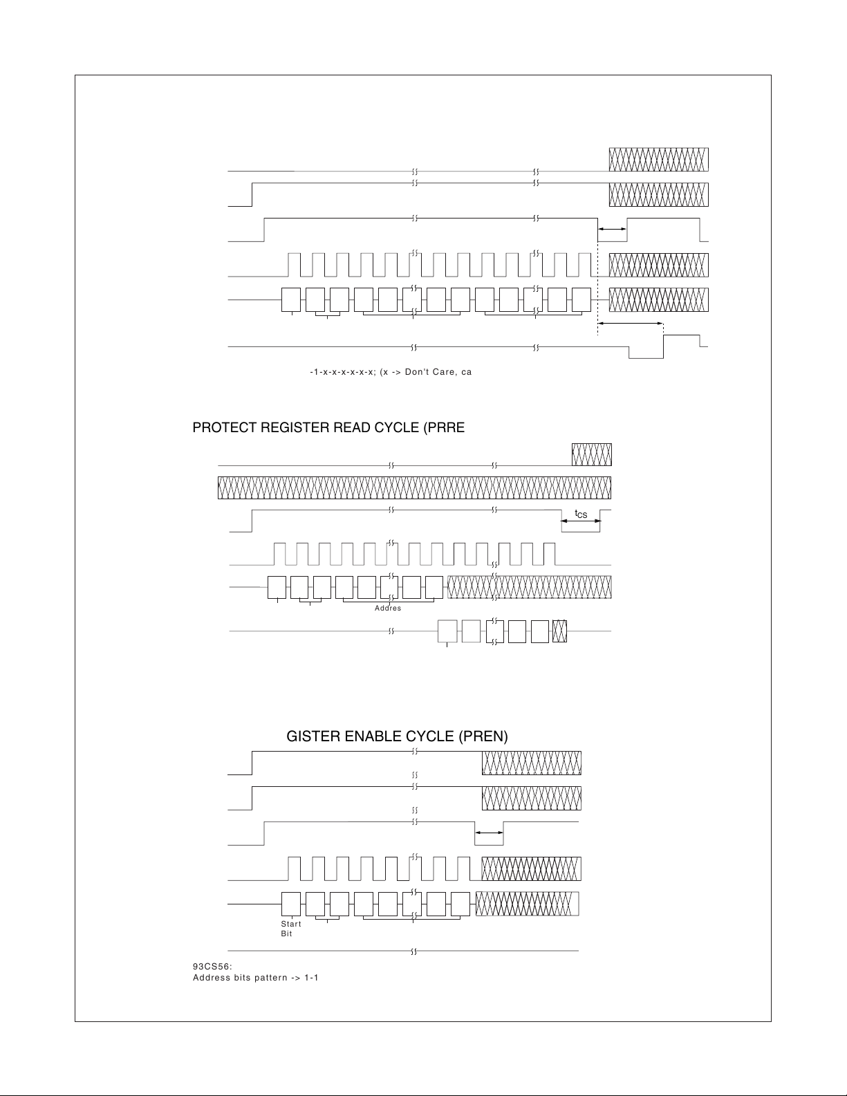
is recommended that no new instruction be issued. Refer
cycle diagram.
Write All
NM93CS56 Rev. F.2
6
www.fairchildsemi.com
Page 7

with Data Protect and Sequential Read
NM93CS56 (MICROWIRE Bus Interface) 2048-Bit Serial EEPROM
5) Write Disable (WDS)
Write Disable (WDS) instruction disables all programming operations and is recommended to follow all programming operations.
Executing this instruction after a valid write instruction would
protect against accidental data disturb due to spurious noise,
glitches, inadvertent writes etc. Input information (Start bit, Opcode
and Address) for this WDS instruction should be issued as listed
under Table1. The device becomes write-disabled at the end of
this cycle when the CS signal is brought low. Execution of a READ
instruction is independent of WDS instruction. Refer
Write Disable
cycle diagram.
Protect Register Instructions
Following five instructions, PRREAD, PREN, PRCLEAR,
PRWRITE and PRDS are specific to operations intended for
Protect Register. The PRE pin should be held high during these
instructions.
1) Protect Register Read (PRREAD)
This instruction reads the content of the internal Protect Register.
Content of this register is 8-bit wide and is the starting address of
the “write-protected” section of the memory array. All memory
locations greater than or equal to this address are write-protected.
Input information (Start bit, Opcode and Address) for this PRREAD
instruction should be issued as listed under Table 1. Upon
receiving a valid input information, decoding of the opcode and the
address is made, followed by data transfer (address information)
from the Protect Register. This 8-bit data is then shifted out on the
DO pin with the MSB first and the LSB last. Like the READ
instruction a dummy-bit (logical 0) precedes this 8-bit data output
string. Output data changes are initiated on the rising edge of the
SK clock. After reading the 8-bit data, the CS signal can be brought
low to end the PRREAD cycle. The PRE pin should be held high
during this cycle. Refer
Though the content of this register is 8-bit wide, only the last 7 bits
(LSB) are valid for NM93CS56 device.
Protect Register Read cycle diagram.
2) Protect Register Enable (PREN)
This instruction is required to enable PRCLEAR, PRWRITE and
PRDS instructions and should be executed prior to executing
PRCLEAR, PRWRITE and PRDS instructions. However, this
PREN instruction is enabled (valid) only the following are true
■ Device is write-enabled (Refer WEN instruction)
■ PE pin is held high during this cycle
■ PRE pin is held high during this cycle
Input information (Start bit, Opcode and Address) for this PREN
instruction should be issued as listed under Table1. The Protect
Register becomes enabled for PRCLEAR, PRWRITE and PRDS
instructions at the end of this cycle when the CS signal is brought
low. Note that this PREN instruction must immediately precede
a PRCLEAR, PRWRITE or PRDS instruction. In other words, no
other instruction should be executed between a PREN instruction
and a PRCLEAR, PRWRITE or PRDS instruction. Refer
Protect
Register Enable cycle diagram.
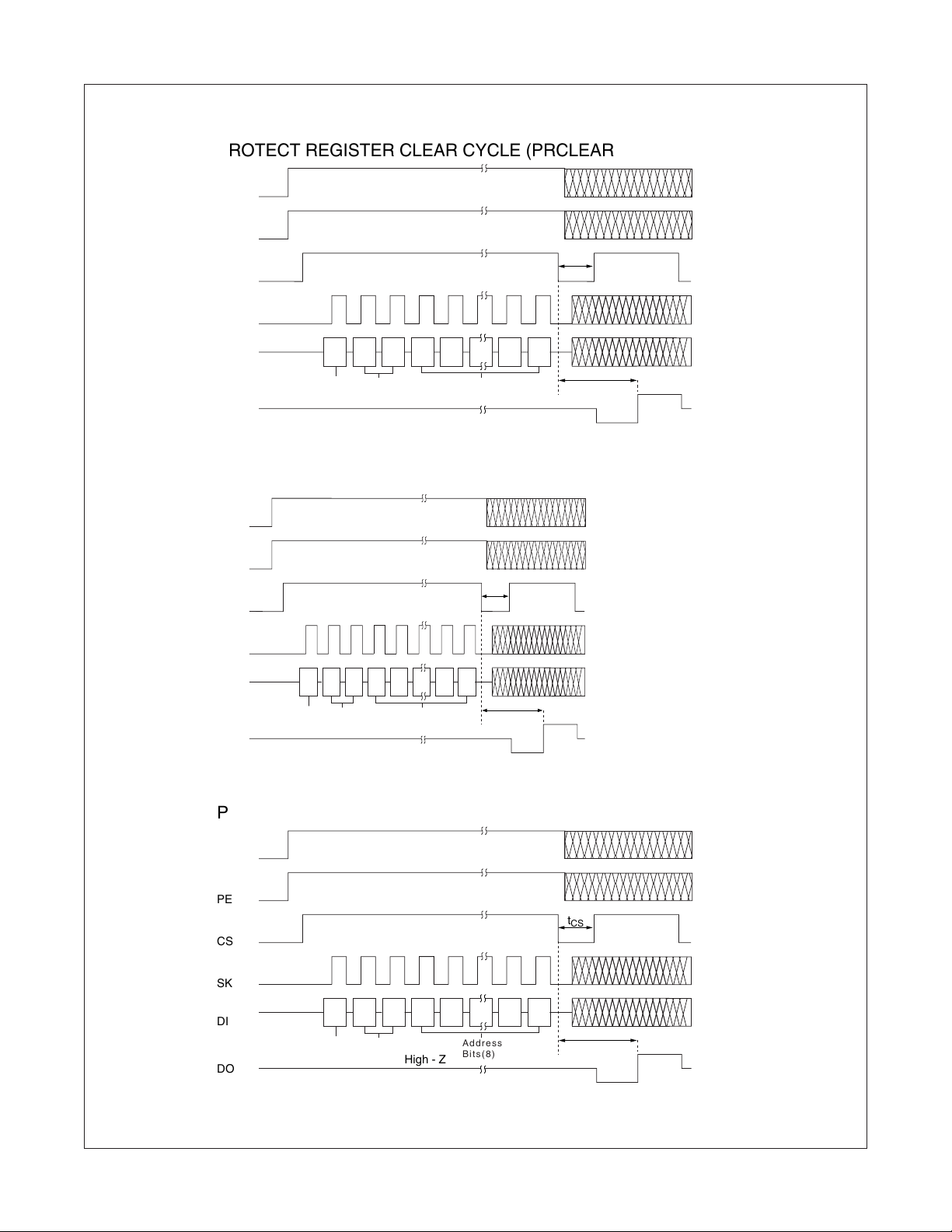
3) Protect Register Clear (PRCLEAR)
This instruction clears the content of the Protect register and
therefore enables write operations (WRITE or WRALL) to all
memory locations. Executing this instruction will program the
content of the Protect Register with a pattern of all 1s. However,
in this case, WRITE operation to the last memory address
(0x01111111) is still enabled. PRCLEAR instruction is enabled
(valid) only when the following are true:
■ PREN instruction was executed immediately prior to
PRCLEAR instruction
■ PE pin is held high during this cycle
■ PRE pin is held high during this cycle
Input information (Start bit, Opcode and Address) for this PRCLEAR
instruction should be issued as listed under Table1. After inputting
the last bit of address (A0 bit), CS signal must be brought low
before the next rising edge of the SK clock. This falling edge of the
CS initiates the self-timed clear cycle. It takes tWP time (Refer
appropriate DC and AC Electrical Characteristics table) for the
internal clear cycle to finish. During this time, the device remains
busy and is not ready for another instruction. Status of the internal
programming can be polled as described under WRITE instruction
description. While the device is busy, it is recommended that no
new instruction be issued. Refer
Protect Register Clear cycle
diagram.
4) Protect Register Write (PRWRITE)
This instruction is used to write the starting address of the memory
section to be write-protected into the Protect register. After the
execution of PRWRITE instruction, all memory locations greater
than or equal to this address are write-protected. PRWRITE
instruction is enabled (valid) only the following are true:
■ PRCLEAR instruction was executed first (to clear the Protect
Register)
■ PREN instruction was executed immediately prior to
PRWRITE instruction
■ PE pin is held high during this cycle
■ PRE pin is held high during this cycle
Input information (Start bit, Opcode and Address) for this PRWRITE
instruction should be issued as listed under Table1. After inputting
the last bit of address (A0 bit), CS signal must be brought low
before the next rising edge of the SK clock. This falling edge of the
CS initiates the self-timed programming cycle. It takes tWP time
(Refer appropriate DC and AC Electrical Characteristics table) for
the internal programming cycle to finish. During this time, the
device remains busy and is not ready for another instruction.
Status of the internal programming can be polled as described
under WRITE instruction description. While the device is busy, it
is recommended that no new instruction be issued. Refer
Protect
Register Write cycle diagram.
5) Protect Register Disable (PRDS)
Unlike all other instructions, this instruction is a one-time-only
instruction which when executed permanently write-protects
the Protect Register and renders it unalterable in the future. This
instruction is useful to safeguard vital data (typically read only
data) in the memory against any possible corruption. PRDS
instruction is enabled (valid) only the following are true:
■ PREN instruction was executed immediately prior to PRDS
instruction
■ PE pin is held high during this cycle
■ PRE pin is held high during this cycle
Input information (Start bit, Opcode and Address) for this PRDS
NM93CS56 Rev. F.2
7
www.fairchildsemi.com
Page 8

with Data Protect and Sequential Read
NM93CS56 (MICROWIRE Bus Interface) 2048-Bit Serial EEPROM
instruction should be issued as listed under Table1. After inputting
the last bit of address (A0 bit), CS signal must be brought low
before the next rising edge of the SK clock. This falling edge of the
CS initiates the self-timed programming cycle. It takes tWP time
(Refer appropriate DC and AC Electrical Characteristics table) for
the internal programming cycle to finish. During this time, the
device remains busy and is not ready for another instruction.
Status of the internal programming can be polled as described
under WRITE instruction description. While the device is busy, it
is recommended that no new instruction be issued. The Protect
Register is permanently write-protected at the end of this cycle.
Protect Register Disable cycle diagram.
Refer
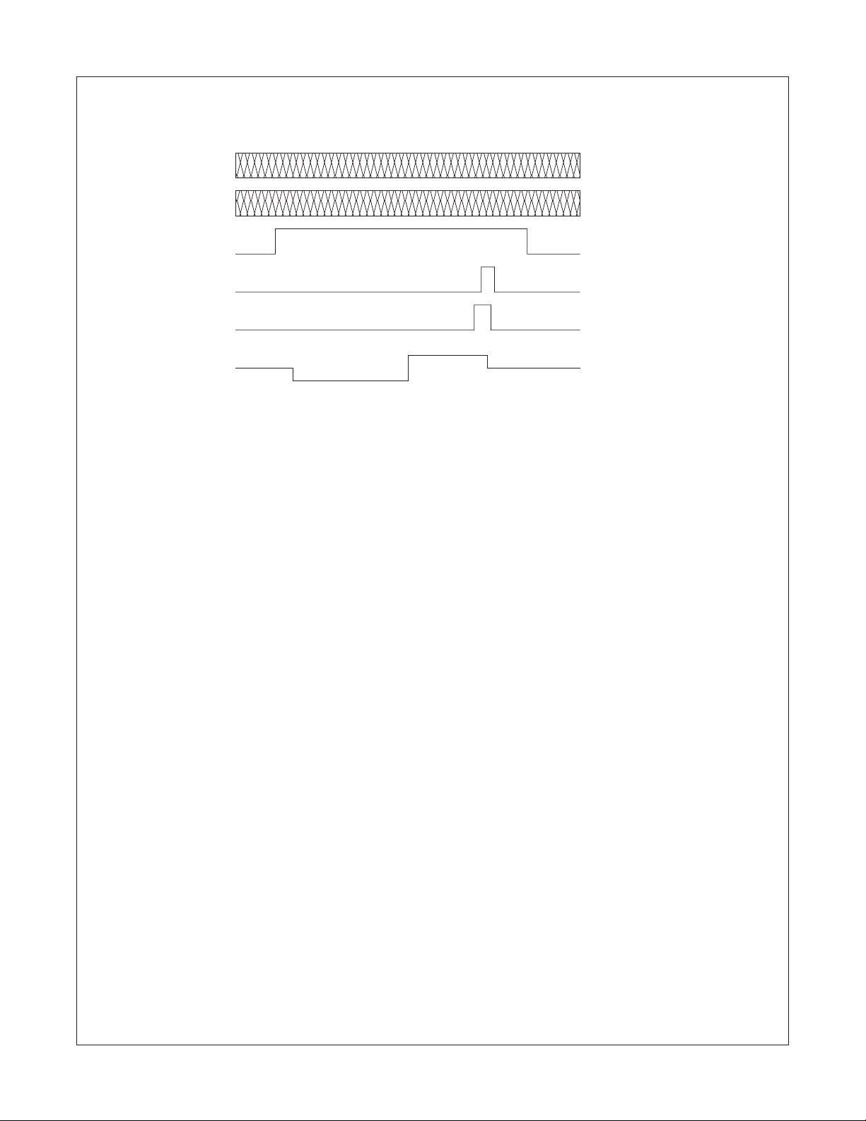
Clearing of Ready/Busy status
When programming is in progress, the Data-Out pin will display
the programming status as either BUSY (low) or READY (high)
when CS is brought high (DO output will be tri-stated when CS is
low). To restate, during programming, the CS pin may be brought
high and low any number of times to view the programming status
without affecting the programming operation. Once programming
is completed (Output in READY state), the output is ‘cleared’
(returned to normal tri-state condition) by clocking in a Start Bit.
After the Start Bit is clocked in, the output will return to a tri-stated
condition. When clocked in, this Start Bit can be the first bit in a
command string, or CS can be brought low again to reset all
internal circuits. Refer
Clearing Ready Status
diagram.
Related Document
Application Note: AN758 - Using Fairchild’s MICROWIRE™ EEPROM.
NM93CS56 Rev. F.2
8
www.fairchildsemi.com
Page 9
;
;
;
Timing Diagrams
SYNCHRONOUS DATA TIMING
with Data Protect and Sequential Read
NM93CS56 (MICROWIRE Bus Interface) 2048-Bit Serial EEPROM
CS
SK
t
t
PRES
SKS
t
CSS
t
SKH
t
PRE
t
PES
PE
t
DIStDIH
Valid
DI
Input
t
PD
DO (Data Read)
t
SV
DO (Status Read)
NORMAL READ CYCLE (READ)
PRE
PE
CS
SKL
Valid
Input
Valid
Output
t
CSH
t
PREH
t
PEH
t
t
PD
DH
Valid
Output
t
DF
t
DF
Valid Status
t
CS
SK
DI
DO
93CS56:
Address bits pattern -> x-A6-A5-A4-A3-A2-A1-A0; (x -> Don't Care, can be 0 or 1); ( A6-A0 -> User defined )
1 1 0 A7 A6 A1 A0
High - Z
Address
Bits(8)
Start
Bit
Opcode
Bits(2)
D15 D1 D0
0
Dummy
Bit
SEQUENTIAL READ CYCLE (PRE = 0; PE = X)
PRE
t
CS
CS
SK
DI
DO
93CS56:
Address bits pattern ->x-A6-A5-A4-A3-A2-A1-A0; (x -> Don't Care, can be 0 or 1); ( A6-A0 -> User defined )
1 1 0 A7 A0
High - Z
Address
Bits(8)
Start
Bit
Opcode
Bits(2)
0
Dummy
Bit
D15 D0
Data(n)
D15 D0 D15 D0
Data(n+1) Data(n+2)
NM93CS56 Rev. F.2
9
www.fairchildsemi.com
Page 10
Timing Diagrams (Continued)
WRITE ENABLE CYCLE (WEN)
PRE
PE
CS
SK
DI
DO
93CS56:
Address bits pattern -> 1-1-x-x-x-x-x-x; (x -> Don't Care, can be 0 or 1)
WRITE DISABLE CYCLE (WDS)
PRE
1 0 0 A7 A6 A1 A0
Start
Opcode
Bit
Bits(2)
Address
Bits(8)
High - Z
with Data Protect and Sequential Read
NM93CS56 (MICROWIRE Bus Interface) 2048-Bit Serial EEPROM
t
CS
PE
t
CS
CS
SK
DI
DO
93CS56:
Address bits pattern -> 0-0-x-x-x-x-x-x; (x -> Don't Care, can be 0 or 1)
1 0 0 A7 A6 A1 A0
Start
Bit
Opcode
Bits(2)
Address
Bits(8)
High - Z
WRITE CYCLE (WRITE)
PRE
PE
t
CS
CS
SK
DI
DO
93CS56:
Address bits pattern -> x-A6-A5-A4-A3-A2-A1-A0; (x -> Don't Care, can be 0 or 1); ( A6-A0 -> User defined )
Data bits pattern -> User defined
1 0 1 A7 A6 A1 A0 D15 D14 D1 D0
Start
Bit
Opcode
Bits(2)
Address
Bits(8)
High - Z
Data
Bits(16)
t
WP
Ready
Busy
NM93CS56 Rev. F.2
10
www.fairchildsemi.com
Page 11
Timing Diagrams (Continued)
WRITE ALL CYCLE (WRALL)
PRE
PE
CS
SK
with Data Protect and Sequential Read
NM93CS56 (MICROWIRE Bus Interface) 2048-Bit Serial EEPROM
t
CS
DI
DO
93CS56:
Address bits pattern -> 0-1-x-x-x-x-x-x; (x -> Don't Care, can be 0 or 1)
Data bits pattern -> User defined
1 0 0 A7 A6 A1 A0 D15 D14 D1 D0
Start
Bit
Opcode
Bits(2)
Address
Bits(8)
High - Z
Data
Bits(16)
PROTECT REGISTER READ CYCLE (PRREAD)
PRE
PE
CS
SK
DI
DO
93CS56:
Address bits pattern -> x-x-x-x-x-x-x-x; (x -> Don't Care, can be 0 or 1)
1 1 0 A7 A6 A1 A0
Start
Bit
Opcode
Bits(2)
High - Z
Address
Bits(8)
D7 D1 D0
0
Dummy
Bit
t
WP
Ready
Busy
t
CS
NM93CS56 Rev. F.2
PROTECT REGISTER ENABLE CYCLE (PREN)
PRE
PE
t
CS
CS
SK
DI
DO
93CS56:
Address bits pattern -> 1-1-x-x-x-x-x-x; (x -> Don't Care, can be 0 or 1)
1 0 0 A7 A6 A1 A0
Start
Bit
Opcode
Bits(2)
Address
Bits(8)
11
High - Z
www.fairchildsemi.com
Page 12
Timing Diagrams (Continued)
PROTECT REGISTER CLEAR CYCLE (PRCLEAR)
PRE
PE
CS
SK
with Data Protect and Sequential Read
NM93CS56 (MICROWIRE Bus Interface) 2048-Bit Serial EEPROM
t
CS
DI
DO
93CS56:
Address bits pattern -> 1-1-1-1-1-1-1-1
1 1 1 A7 A6 A1 A0
Start
Bit
Opcode
Bits(2)
High - Z
Address
Bits(8)
t
WP
Ready
Busy
PROTECT REGISTER WRITE CYCLE (PRWRITE)
PRE
PE
t
CS
CS
SK
DI
DO
93CS56:
Address bits pattern -> x-A6-A5-A4-A3-A2-A1-A0; (x -> Don't Care, can be 0 or 1); ( A6-A0 -> User defined )
1 0 1 A7 A6 A1 A0
High - Z
Address
Bits(8)
Start
Bit
Opcode
Bits(2)
t
WP
Busy
Ready
NM93CS56 Rev. F.2
PROTECT REGISTER DISABLE CYCLE (PRDS)
PRE
PE
t
CS
CS
SK
DI
DO
93CS56:
Address bits pattern -> 0-0-0-0-0-0-0-0
1 0 0 A7 A6 A1 A0
Start
Bit
Opcode
Bits(2)
High - Z
Address
Bits(8)
12
t
WP
Busy
Ready
www.fairchildsemi.com
Page 13
Timing Diagrams (Continued)
CLEARING READY STATUS
PRE
PE
CS
SK
with Data Protect and Sequential Read
NM93CS56 (MICROWIRE Bus Interface) 2048-Bit Serial EEPROM
DI
DO
Note: This Start bit can also be part of a next instruction. Hence the cycle
can be continued(instead of getting terminated, as shown) as if a new
instruction is being issued.
High - Z High - Z
Busy
Ready
Start
Bit
NM93CS56 Rev. F.2
13
www.fairchildsemi.com
Page 14
Physical Dimensions inches (millimeters) unless otherwise noted
0.189 - 0.197
(4.800 - 5.004)
8765
0.228 - 0.244
(5.791 - 6.198)
1234
Lead #1
IDENT
with Data Protect and Sequential Read
NM93CS56 (MICROWIRE Bus Interface) 2048-Bit Serial EEPROM
0.010 - 0.020
(0.254 - 0.508)
0.0075 - 0.0098
(0.190 - 0.249)
Typ. All Leads
x 45°
0.150 - 0.157
(3.810 - 3.988)
0.04
(0.102)
All lead tips
8° Max, Typ.
All leads
0.016 - 0.050
(0.406 - 1.270)
Typ. All Leads
0.053 - 0.069
(1.346 - 1.753)
0.014
(0.356)
0.050
(1.270)
Typ
Molded Package, Small Outline, 0.15 Wide, 8-Lead (M8)
Package Number M08A
0.004 - 0.010
(0.102 - 0.254)
Seating
Plane
0.014 - 0.020
(0.356 - 0.508)
Typ.
NM93CS56 Rev. F.2
14
www.fairchildsemi.com
Page 15
Physical Dimensions inches (millimeters) unless otherwise noted
0.114 - 0.122
(2.90 - 3.10)
85
0.246 - 0.256
(6.25 - 6.5)
0.123 - 0.128
(3.13 - 3.30)
0.0433
Max
(1.1)
0.0256 (0.65)
Typ.
14
Pin #1 IDENT
0.169 - 0.177
(4.30 - 4.50)
0.002 - 0.006
(0.05 - 0.15)
0.0075 - 0.0098
(0.19 - 0.30)
DETAIL A
Typ. Scale: 40X
(1.78) Typ
(0.42) Typ
Land pattern recommendation
See detail A
0°-8°
0.020 - 0.028
(0.50 - 0.70)
Seating
(4.16) Typ
(0.65) Typ
plane
(7.72) Typ
0.0035 - 0.0079
Gage
plane
0.0075 - 0.0098
(0.19 - 0.25)
with Data Protect and Sequential Read
NM93CS56 (MICROWIRE Bus Interface) 2048-Bit Serial EEPROM
Notes: Unless otherwise specified
1. Reference JEDEC registration MO153. Variation AA. Dated 7/93
8-Pin Molded TSSOP, JEDEC (MT8)
Package Number MTC08
NM93CS56 Rev. F.2
15
www.fairchildsemi.com
Page 16
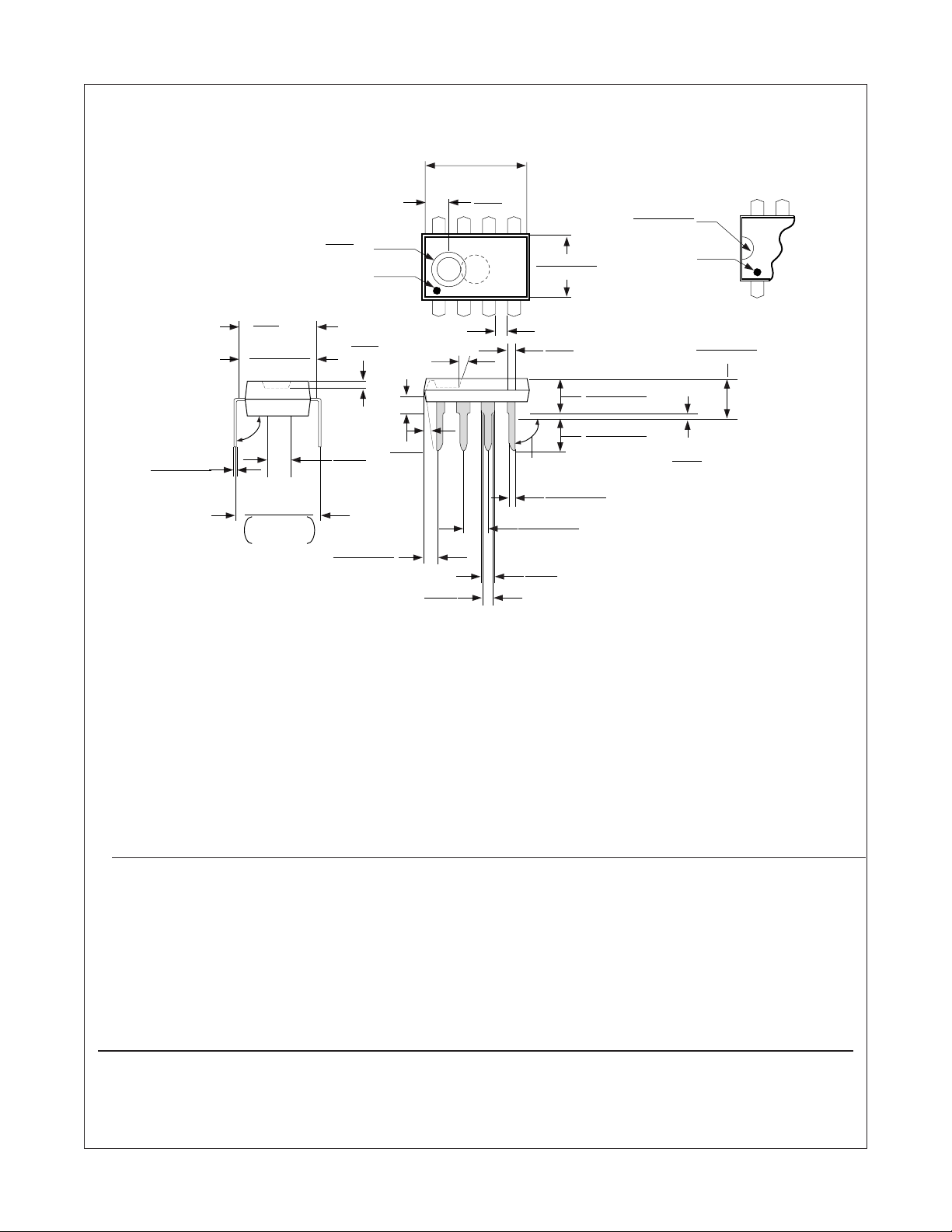
Physical Dimensions inches (millimeters) unless otherwise noted
0.373 - 0.400
(9.474 - 10.16)
0.090
(2.286)
8765
1234
0.040
(1.016)
20° ± 1°
0.065
(1.651)
0.050
(1.270)
+
Typ.
0.250 - 0.005
(6.35 ± 0.127)
0.039
(0.991)
0.130 ± 0.005
(3.302 ± 0.127)
0.125 - 0.140
(3.175 - 3.556)
90° ± 4°
Typ
0.018 ± 0.003
(0.457 ± 0.076)
0.100 ± 0.010
(2.540 ± 0.254)
0.060
(1.524)
95° ± 5°
0.009 - 0.015
(0.229 - 0.381)
0.280
MIN
(7.112)
0.300 - 0.320
(7.62 - 8.128)
+0.040
0.325
-0.015
+1.016
8.255
-0.381
0.092
DIA
(2.337)
Pin #1 IDENT
0.030
(0.762)
0.125
(3.175)
DIA
NOM
0.045 ± 0.015
(1.143 ± 0.381)
Option 1
MAX
0.032 ± 0.005
(0.813 ± 0.127)
RAD
Pin #1
IDENT
0.020
(0.508)
Min
Option 2
0.145 - 0.200
(3.683 - 5.080)
87
1
with Data Protect and Sequential Read
NM93CS56 (MICROWIRE Bus Interface) 2048-Bit Serial EEPROM
Molded Dual-In-Line Package (N)
Package Number N08E
Life Support Policy
Fairchild's products are not authorized for use as critical components in life support devices or systems without the express written
approval of the President of Fairchild Semiconductor Corporation. As used herein:
1. Life support devices or systems are devices or systems which,
(a) are intended for surgical implant into the body, or (b) support
or sustain life, and whose failure to perform, when properly
used in accordance with instructions for use provided in the
labeling, can be reasonably expected to result in a significant
injury to the user.
Fairchild Semiconductor Fairchild Semiconductor Fairchild Semiconductor Fairchild Semiconductor
Americas Europe Hong Kong Japan Ltd.
Customer Response Center Fax: +44 (0) 1793-856858 8/F, Room 808, Empire Centre 4F, Natsume Bldg.
Tel. 1-888-522-5372 Deutsch Tel: +49 (0) 8141-6102-0 68 Mody Road, Tsimshatsui East 2-18-6, Yushima, Bunkyo-ku
English Tel: +44 (0) 1793-856856 Kowloon. Hong Kong Tokyo, 113-0034 Japan
Français Tel: +33 (0) 1-6930-3696 Tel; +852-2722-8338 Tel: 81-3-3818-8840
Italiano Tel: +39 (0) 2-249111-1 Fax: +852-2722-8383 Fax: 81-3-3818-8841
2. A critical component is any component of a life support device
or system whose failure to perform can be reasonably expected to cause the failure of the life support device or system,
or to affect its safety or effectiveness.
Fairchild does not assume any responsibility for use of any circuitry described, no circuit patent licenses are implied and Fairchild reserves the right at any time without notice to change said circuitry and specifications.
16
NM93CS56 Rev. F.2
www.fairchildsemi.com
 Loading...