

Page 1
NJU6355
SERIAL I/O REAL TIME CLOCK
■GENERAL DESCRIPTION ■PACKAGE OUTLINE
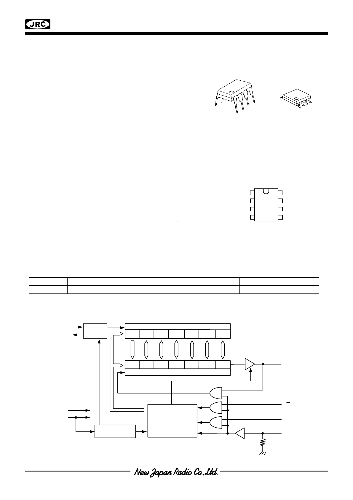
The NJU6355 series is a s erial I/O real time clock s uitable
for 4 bits microprocessor.
It contains quartz crystal oscillator, counter, shift register,
voltage regulator, voltage detector and interface controller.
The NJU6355 series required only 4-port of micropr ocessor
for data transfer, and the microprocessor can receiv e the data
at any time when the microprocessor requires.
The operating voltage is as wide as 2.0V to 5.5V,
consequently, the NJU6355 series can count accurate time
data even if the back up period.
Furthermore, the long time back up is available as the
operating current during the back up period is less than
3uA(TYP).
■FEATURES ■PIN CONFIGURATION
●Low Operating Voltage 2.0 to 3.6V
●Low Operating Current 3.0uA (TYP) @2.0V
3.0uA (TYP) @3.0V
4.0uA (TYP) @5.0V
●BCD Counts of Seconds, Minutes, Hours, Days of Week
Day, Month and Year
●Required only 4-port DATA, CLK, CE and I/O
●Low Battery Detector Low Voltage Alarm Signal Output
●Automatic Leap Year Compensation Up to AD 2099
●Package Outline DIP8 / DMP8
●C-MOS T echnology
■LINE-UP TABLE
Type No. Output Data Oscillation Capacitor
NJU6355 E Seconds, Minutes, Hours, Days of Week, Day, Month, Year Cd=21pF / Cg=21pF on Chip
■BLOCK DIAGRAM
NJU6355ED NJU6355EM
I/O
XT
XT
VSS
VDD
DATA
CLK
CE
VSS
V
DD
XT
XT
Oscillat o r
Divider
Voltage Detector
Sec. Min. Hr.
Sec. Min. Hr. Day Month Year
Timer Counter
Days of
Week
Days of
Week
Shift Register
Contr olle r
&
Clock Counter
Day Month Year
DATA
I/O
CLK
CE
-1 -
Page 2
NJU6355
■TREMINAL DESCRIPTION
No. SYMBOL FUNCTION
I/O Input/Output Select Terminal for DATA Terminal
1
2 XT
3
5 CE
6 CLK
7 DATA
8 VDD
4 VSS
■FUNCTIONAL DESCRIPTION
1. Timer Dat a Structure
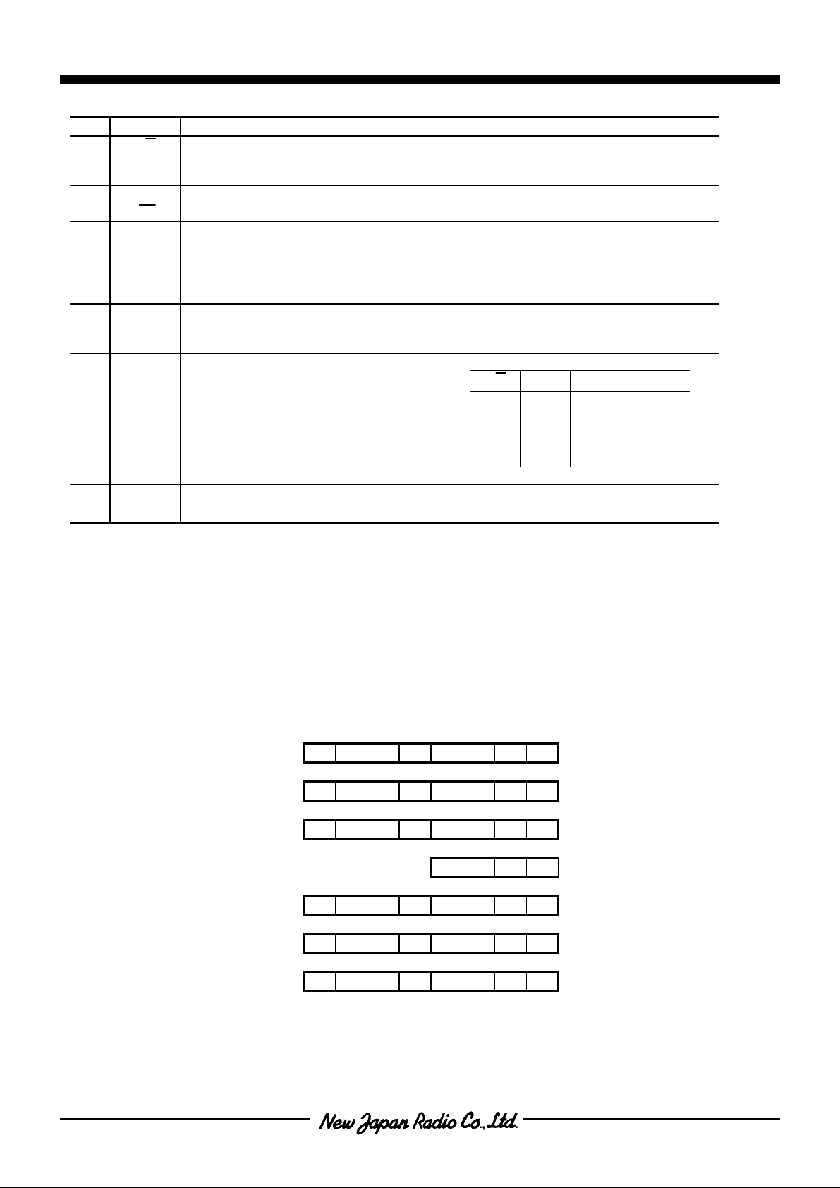
The NJU6355 using BCD c ode which consisting of 4 bits per 1 digit. The calender function including the last
date of each m onth and the leap year calculation is executed autom atically. The unused bit for the timer data is
“0”.
XT
"H" : Input, "L" : Output
During the CE terminal is "L", the DATA terminal is high impedance.
Quartz Crystal Connecting Terminal (f=32.768kHz)
Refer to the line-up table for internal Cg, Cd value.
Chip Enable Input Terminal (with Pull-down Resistance)
"H" : DATA input/output is available.
"L" : DATA terminal is high impedance.
When the CE signal is which rising edge or falling edge,
the CLK signal should be fixed to "L".
Clock Input Terminal
The DATA input/output is synchronized this clock.
When the CE terminal is "L" the DATA terminal is high impedance.
Serial Timer Data Input/Output Terminal
Power Supply
GND
Timer Data Bit Map
MSB LSB Range
Second 0 S6 S5 S4 S3 S2 S1 S0 0 to 59
Minute 0 m6 m5 m4 m3 m2 m1 m0 0 to 59
Hour 0 0 H5 H4 H3 H2 H1 H0 0 to 23
Days of Week 0 W2 W1 W0 1 to 7
Day 0 0 D5 D4 D3 D2 D1 D0 1 to 31
Month 0 0 0 M4 M3 M2 M1 M0 1 to 12
Year Y7 Y6 Y5 Y4 Y3 Y2 Y1 Y0 0 to 99
I/O
H H Input
L H Output
H L High Impedance
L L High Impedance
CE DATA
- 2 -
Page 3
NJU6355
2. Timer Data Reading
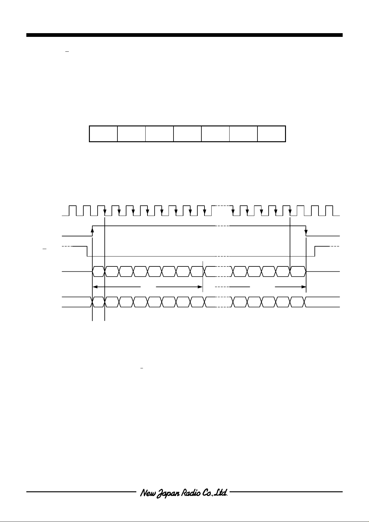
When the I/O termianl is "L" and the CE tarminal is "H " , timer data can read ou t. The output is LS B f irs t and the
output data strings is shown below.
The timer data is transferred from timer counter to shift register at rising edge of the chip enable on the CE
terminal, and output the LSB of the timer data from the DATA terminal.
Afterward the timer data in the shift regis ter shift by synchronized at the f alling edge of cloc k signal on the CLK
terminal and output from the DATA terminal.
If the timer data is updated in t he data output, there are one seco nd difference between timer data and ou tput
data.
Type E
Year Month Day
The data is read out from LSB of Year, and first 52-bit is effective.
If the low voltage detec tor detect the lo w b atter y, (EE)
code of (EE)
is a warning for the broken.
H
< Read Out Timing >
CLK
CE
I/O
Data
Output
Shift
Register
(1) (2)
1 2 3 4 5 6 7 3 4 5 6 7 0
Year Second
1 2 3 4 5 6 7 3 4 5 6 7
0
The timer data is transf erred to the shift register at risi ng edge of the CE (1)
and LSB of the timer data is output to the DATA terminal. Afterward the
timer data in the shift register shift by sync hronized at falling edge of the
CLK(2) then outp ut to the DATA terminal time-to-tim e.
Note) When the CE signal is which rising edge or falling edge,
the CLK signal should be fixed to “L”. And so, before the
CE signal is raised, the I/O signal should be fixed to “L”.
Days of
Week
is written into eac h digit o f tim er data and r ead o ut. The
H
Hour Minute Second
-3 -
Page 4
NJU6355
3. Timer Data Writing
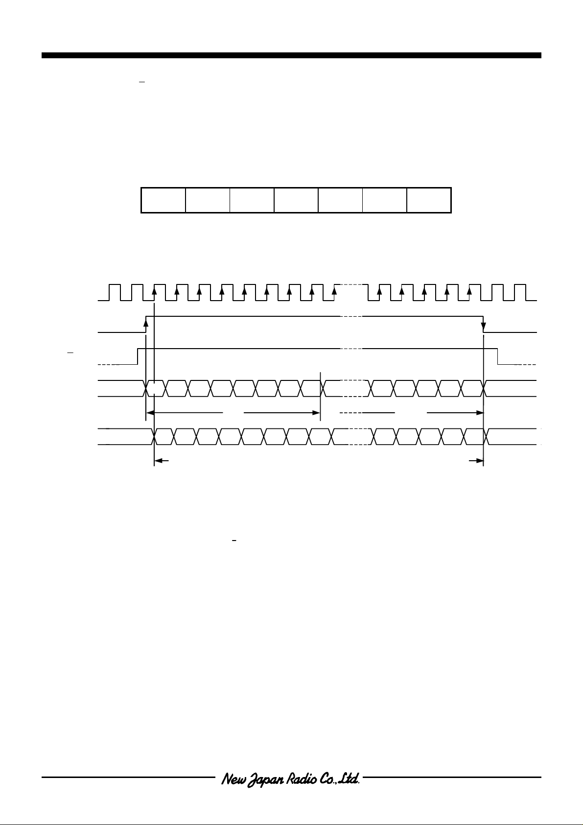
When both of the I/O term inal and the CE terminal are "H", upd ate is stopped, the oscillator d ivider is cleared,
and the timer data can be written to the NJU6355.
The timer data is written into the shift register from the DATA terminal by sync hronized with rising edge of the
clock signal input from the CLK terminal, a nd the data is transferred from the shift register to the tim er counter b y
synchronized with falling edge of the CE signal. In this time the second-counter is cleared to "0", and the oscillator
divider start the operation.
The input data strings are LSB first of each digit as shown below.
Type E
Year Month Day
The data is read out from LSB of Year, and last 44-bit is effective.
< Write Down Timing >
CLK
CE
I/O
Data
Input
Shift
Register
0
2 3 4 5 6 7 3 4 5 6 7
1
Year
1 2 3 4 5 6 7 0 3 4 5 6 7
The data is input into the shift
register at rising edge of the
CLK.
Note) When the CE signal is which rising edge or falling edge,
the CLK signal should be fixed to "L". And so, before the
CE signal is raised, the I/O signal should be fixed to "H".
4. Low Voltage Detector
The NJU6355 series incor porate the low battery detector. If the supply voltage reduce to the detection level,
(EE)
is written into each digit of the shift register as warning code for the CPU.
H
5. Data Access
The NJU6355 series can o per ate f r om 2.0V t o 5 .5 V. However, it is not allow the data acc es s out of th e ra ng e of
5V±10%. It may be broken the data unless 5V±10%.
Thus, when the data acc es s , the CE ter minal should be "H" after the po wer s upp l y rise to 5V±10%, then start the
operation.
Days of
Week
Hour Minute Second
Minute
The data in the shift register is
transferred to the timer counter at this
falling edge of the CE, then the
oscillator divider start the oper ation.
- 4 -
Page 5
NJU6355
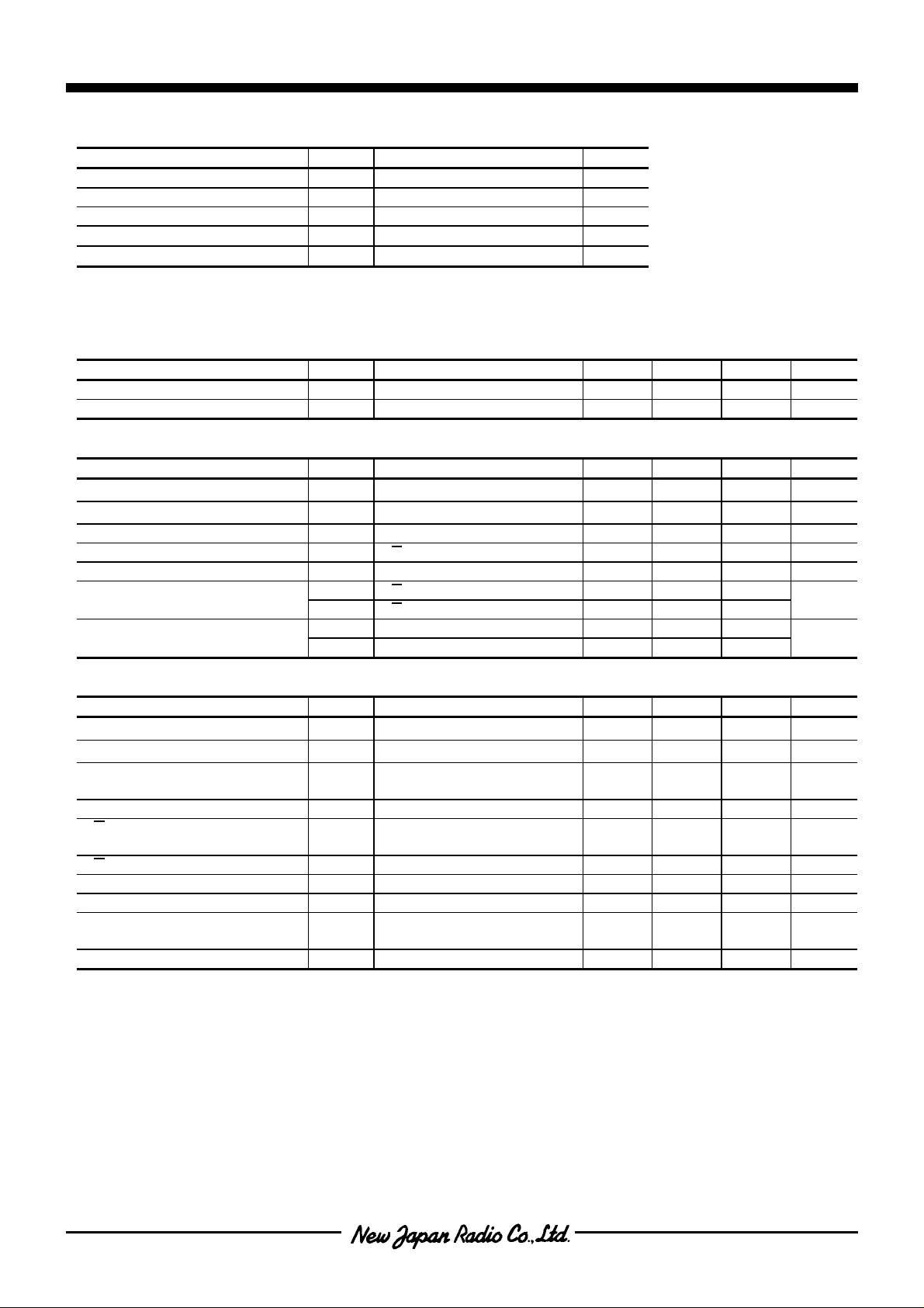
■ABSOLUTE MAXIMUM RATINGS
(Ta=25°C)
PARAMETER SYMBOL RATING UNIT
Supply Voltage VDD -0.3 to +6.0 V
Input Voltage VIN V
Power Dissipation PD 250(DIP8) 200(DMP8) mW
Operating Temperature Range Topr -30 to +80
Storage Temperature Range Tstg -55 to +150
■ELECTRICAL CHARACTERISTICS
DC Characteristics (V
PARAMETER SYMBOL CONDITIONS MIN TYP MAX UNIT
Operating Current IDD XT=32.768kHz, CE=0V 3.0 4.0 uA
Low Battery Detect Voltage V
1.1 1.7 V
DET
PARAMETER SYMBOL CONDITIONS MIN TYP MAX UNIT
Operating Voltage VDD 4.5 5.5 V
Operating Current IDD XT=32.768kHz, CE=0V 4 15 uA
3-st. Leakage Current I
DATA (CE=0V) -2.0 2.0 uA
TSL
Input Leakage Current IIL I/O, CLK -1.0 1.0 uA
Input Current ICE CE (CE=VDD) 20 uA
Input Voltage
Output Voltage
VIH I/O, CE, CLK, DATA 0.8VDD VDD
V
I/O, CE, CLK, DATA VSS 0.2V
IL
VOH DATA (IOH=-0.4mA) 4.1
DATA (IOL=1.0mA) 0.4
V
OL
AC Characteristics (V
PARAMETER SYMBOL CONDITIONS MIN TYP MAX UNIT
CS
CLK Pulse "H" Period t
CLK Pulse "L” Period t
CE Set-up Time Before
CLK Rising
CWH
CWL
t
CE Hold Time After CLK Falling tCH 20 ns
I/O Set-up Time
Before CLK Rising
t
DS
I/O Hold Time After CLK Falling tDH 20 ns
Write Down Data Set-Up Time t
Write Down Data Hold Time t
Data Delay Time
After CLK Falling
100 ns
WDS
20 ns
WDH
t
RDD
Rise/Fall Time tRF 50 ns
-0.3 to VDD+0.3 V
SS
°C
°C
=5.0V±10%, Ta=25°C, CL=50pF)
DD
0.47 5000 us
0.47 5000 us
470 ns
60 ns
200 ns
=2.0V, Ta=25°C)
DD
=5.0V±10%, Ta=25°C)
(V
DD
DD
V
V
-5 -
Page 6
NJU6355
CLK
CE
I/O
(in)
CLK
Input Data
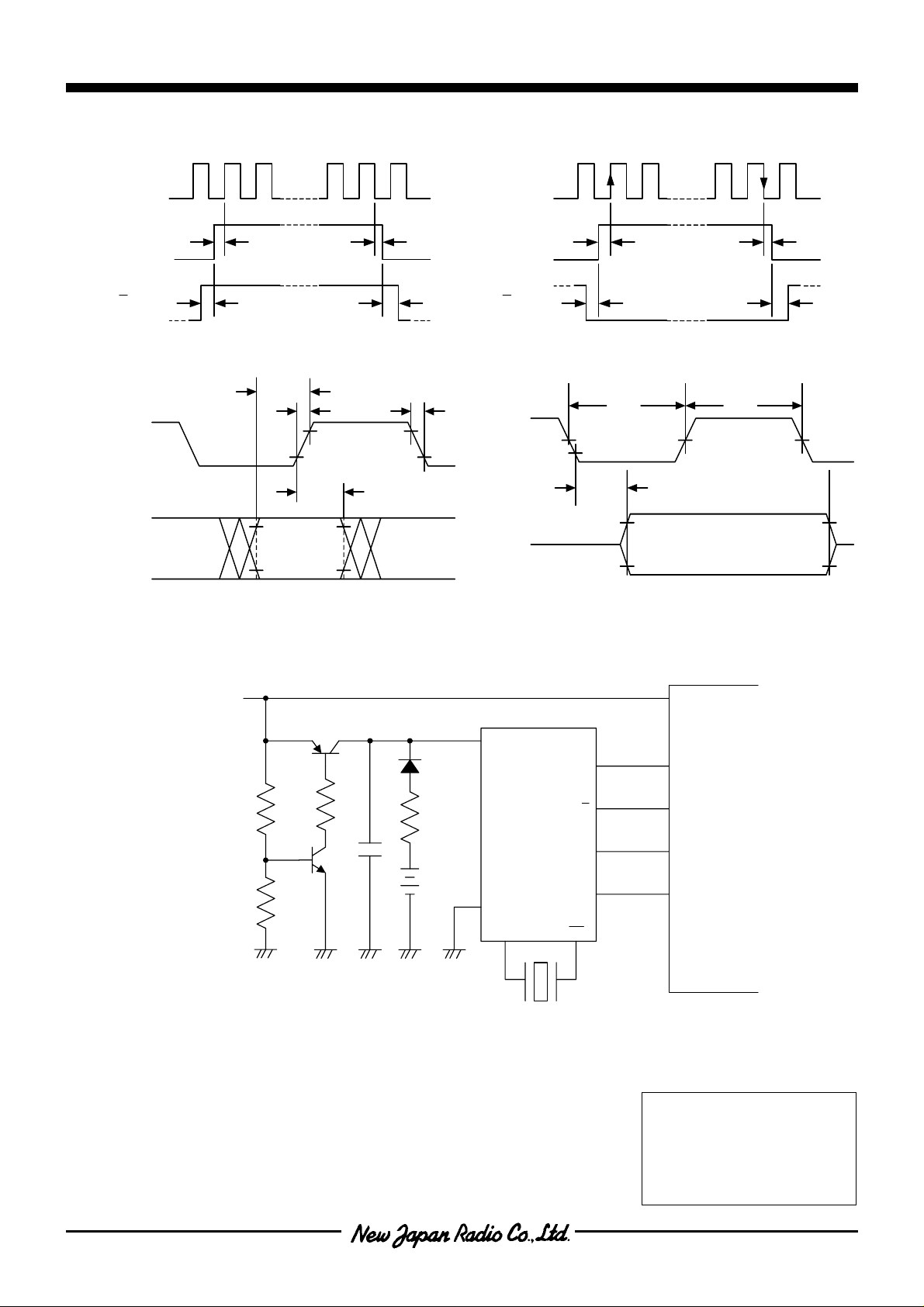
■APPLICATION CIRCUIT
Main Power
Supply
CLK
tCS
t
DS
t
WDS
80%
t
CH
tDH
tr
80%
20%
t
WDH
CE
I/O
(out)
tf
CLK
Vss
50%
20%
t
RDD
80%
t
CS
tDS
t
CWL
50%
t
CH
tDH
t
CWH
50%
80%
Output Data
20%
Vss
20%
VDD
20%
NJU6355
V
DD
DATA
I/O
CPU
CLK
- 6 -
XT
CE
[CAUTION]
The specifications on this data book are only
given for information , without any guarantee
as regards either mistakes or omissions.
The application circuits in this data book are
described only to show representative usages
of the product and not intended for the
guarantee or permission of any right including
the industrial rights.
V
SS
XT
 Loading...