

Page 1
MICROSTEPPING MOTOR CONTROLLER WITH DUAL DAC
■ GENERAL DESCRIPTION ■ PACKAGE OUTLINE
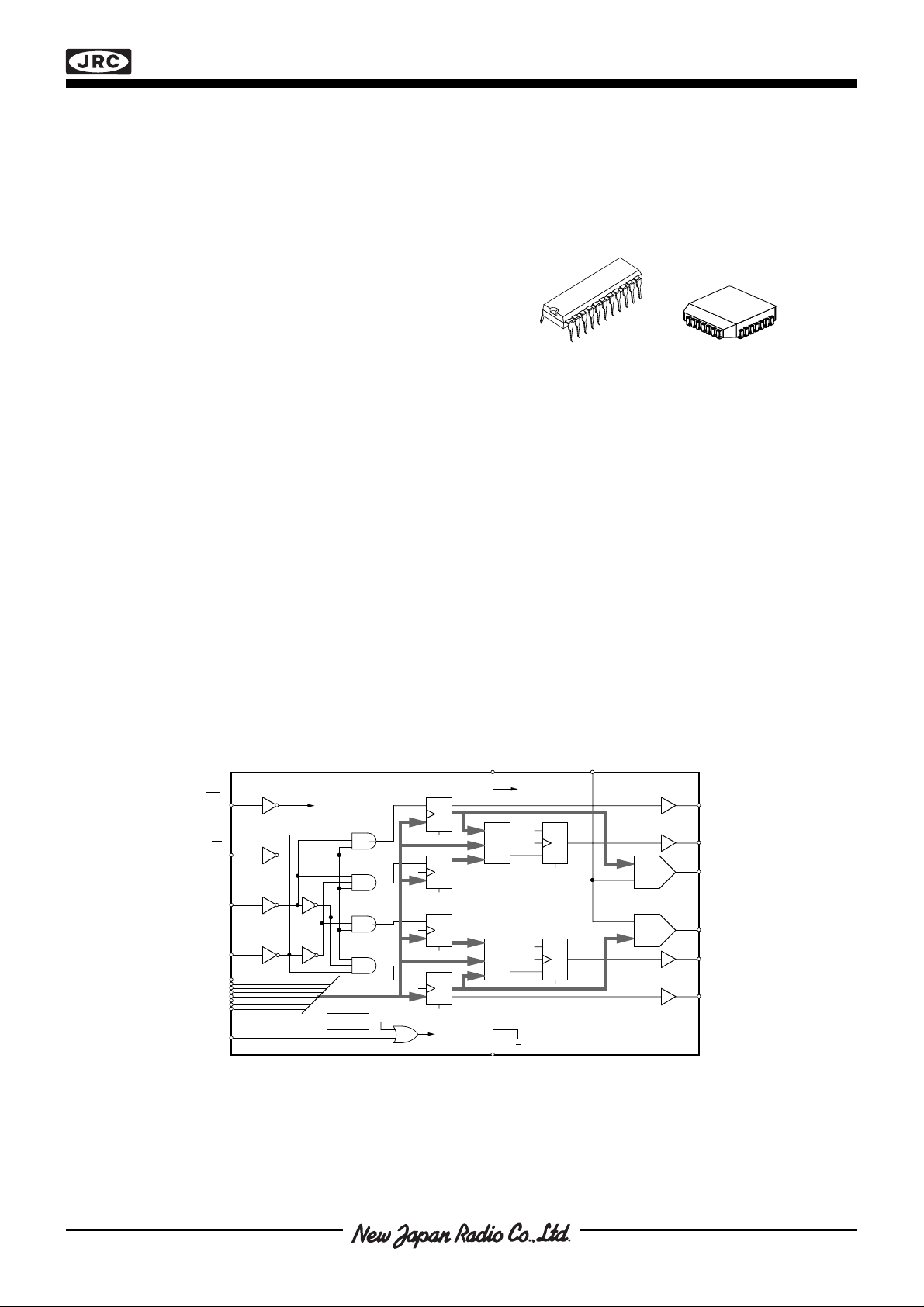
NJU39610 is a dual 7-bit+sign, Digital-to-Analog Converter
(DAC) especially developed to be used together with the
NJM3771, Precision Stepper Motor driver in micro-stepping
applications. The NJU39610 has a set of input registers
connected to an 8-bit data port for easy interfacing directly to
a microprocessor. The NJU39610 is well suited for highspeed micro-stepping application.
NJU39610D2 NJU39610FM2
■ FEATURES
• Analog control voltages from 3 V down to 0.0 V
• High-speed microprocessor interface
NJU39610
• Automatic fast/slow current decay control
• Full-scale error ±1 LSB
• Fast conversion speed 3 µs
• Matches NJM3771
• Packages DIP22/PLCC28
■ BLOCK DIAGRAM
WR
CS
A0
A1
D7 - D0
RESET
POR
V
DD
DA- Data 1
E
C
E1
E2
E3
E4
D
R
Level 1
E
C
D
R
Level 2
E
C
D
R
DA- Data 2
E
C
D
R
R
Digit
Comp
Digit
Comp
E1
E4
C
V
Ref
NJU39610
E
C
D
R
E
D
R
D / A
D / A
Sign
CD
DA
DA
CD
Sign
1
1
1
2
2
2
Figure 1. Block Diagram
V
ss
Page 2
■ PIN CONFIGURATIONS
NJU39610
V
DA
Sign
CD
V
WR
DD
D7
D6
D5
D4
D3
1
ref
2
1
3
1
4
1
5
NJU
39610D2
6
7
8
9
10
11
22
21
20
19
18
17
16
15
14
13
12
Reset
DA
Sign
CD
V
SS
CS
A1
A0
D0
D1
D2
2
2
2
N/C
DA
Reset
N/C
V
DA
N/C
2
ref
1
2
Sign
432
5
6
7
8
39610FM2
9
10
11
12131415161718
1
Sign
2
CD
NJU
1
CD
SS
V
DD
V
CS
1
WR
A0
A1
282726
D7
D6
N/C
N/C
25
D0
24
D1
23
D2
22
N/C
21
D3
20
D4
19
D5
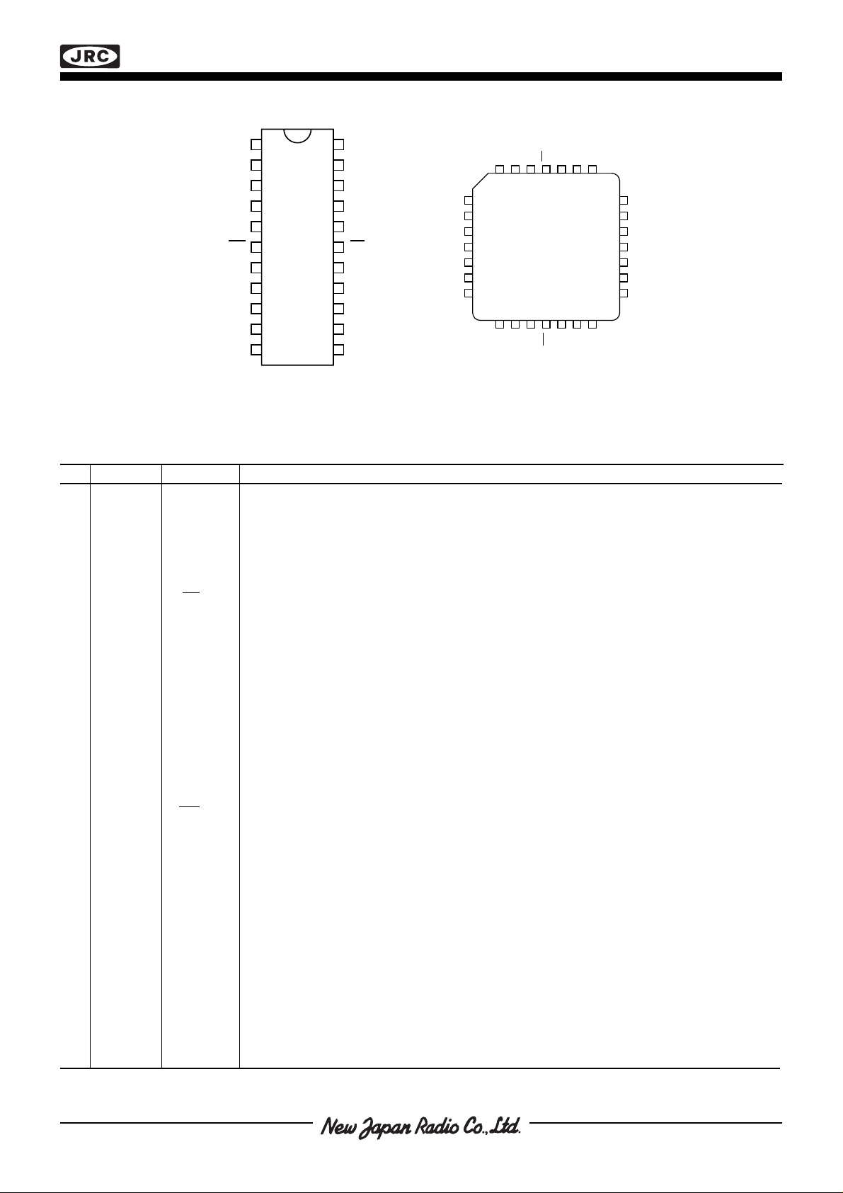
Figure 2. Pin configurations
■ PIN DESCRIPTION
Refer to figure 2.
DIP PLCC Symbol Description
19V
210DA1Digital-to-Analog 1, voltage output. Output between 0.0 V and VR - 1 LSB.
3 12 Sign
Ref
1
413CD1Current Decay 1, TTL/CMOS level. The signal is automatically generated when
514VDDVoltage Drain-Drain, logic supply voltage. Normally +5 V.
6 15 WR Write, TTL/CMOS level, input for writing to internal registers.
7 16 D7 Data 7, TTL/CMOS level, input to set data bit 7 in data word.
8 17 D6 Data 6, TTL/CMOS level, input to set data bit 6 in data word.
9 19 D5 Data 5, TTL/CMOS level, input to set data bit 5 in data word.
10 20 D4 Data 4, TTL/CMOS level, input to set data bit 4 in data word.
11 21 D3 Data 3, TTL/CMOS level, input to set data bit 3 in data word.
12 23 D2 Data 2, TTL/CMOS level, input to set data bit 2 in data word.
13 24 D1 Data 1, TTL/CMOS level, input to set data bit 1 in data word.
14 25 D0 Data 0, TTL/CMOS level, input to set data bit 0 in data word.
15 27 A0 Address 0, TTL/CMOS level, input to select data transfer,
16 28 A1 Address 1, TTL/CMOS level, input to select data transfer. A1 selects between normal
17 1 CS Chip Select, TTL/CMOS level, input to select chip and activate data transfer
18 2 V
19 3 CD
20 4 Sign
21 6 DA
22 7 Reset Reset, digital input resetting internal registers.
SS
2
2
2
5
8
11 N/C Not Connected
18
22
26
Voltage reference supply pin, 2.5 V nominal (3.0 V maximum)
Sign 1, TTL/CMOS level. To be connected directly to NJM3771 Phase input.
Databit D7 is transfered non inverted from NJU39610 data input.
decay level is programmed. LOW level = fast current decay.
Data is clocked into flip flops on positive edge.
A0 selects between cannel 1 (A0 = LOW) and channel 2 (A0 = HIGH).
D/A register programming (A1 = LOW) and decay level register programming (A1 = HIGH).
from data inputs. LOW level = chip is selected.
Voltage Source-Source. Ground pin, 0 V reference for all signals and
measurements unless otherwise noted.
Current Decay 2, TTL/CMOS level. The signal is automatically generated
when decay level is programmed. LOW level = fast current decay .
Sign 2. TTL/CMOS level. To be connected directly to NJM3771 sign input.
Data bit D7 is transfered non-inverted from NJU39610 data input.
Digital-to-Analog 2, voltage output. Output between 0.0 V and V
HIGH level = Reset, V
≥ 3.5 V = HIGH level. Pulled low internally.
Res
- 1 LSB.
ref
Page 3
NJU39610
■ DEFINITION OF TERMS
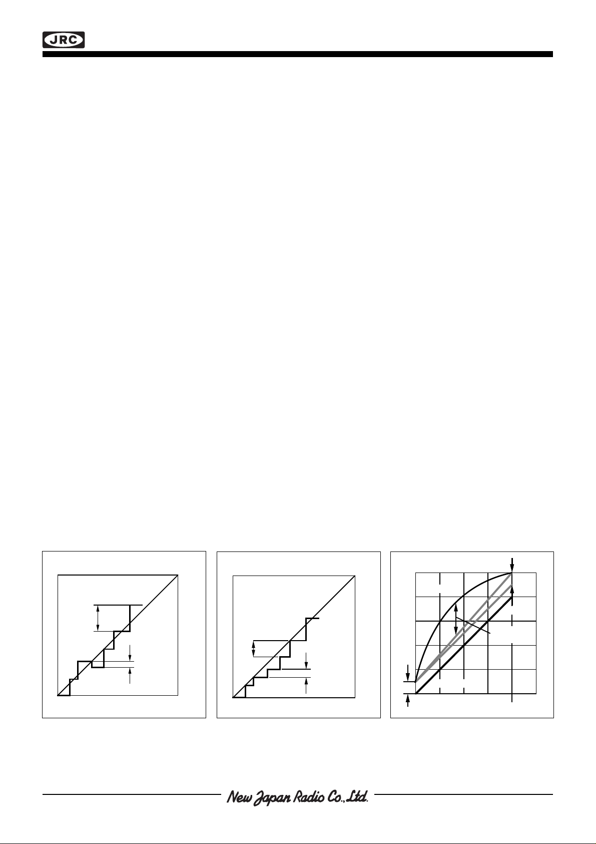
Resolution
Resolution is defined as the reciprocal of the number of discrete steps in the DAC output. It is directly related to the
number of switches or bits within the DAC. For example, NJU39610 has 27, or 128, output levels and therefor has 7
bits resolution. Remember that this is not equal to the number of microsteps available.
Linearity Error
Linearity error is the maximum deviation from a straight line passing through the end points of the DAC transfer
characteristic. It is measured after adjusting for zero and full scale. Linearity error is a parameter intrinsic to the
device and cannot be externally adjusted.
Power Supply Sensitivity
Power supply sensitivity is a measure of the effect of power supply changes on the DAC full-scale output
Settling Time
Full-scale current settling time requires zero-to-full-scale or full-scale-to-zero output change. Settling time is the
time required from a code transition until the DAC output reaches within ±1/2LSB of the final output value.
Full-scale ErrorFull-scale error is a measure of the output error between an ideal DAC and the actual device output.
Differential Non-linearity
The difference between any two consecutive codes in the transfer curve from the theoretical 1LSB, is differential
non-linearity
Monotonic
If the output of a DAC increases for increasing digital input code, then the DAC is monotonic. A 7-bit DAC which is
monotonic to 7 bits simply means that increasing digital input codes will produce an increasing analog output.
NJU39610 is monotonic to 7 bits.
■ FUNCTIONAL DESCRIPTION
Each DAC channel contains two registers, a digital comparator, a flip flop, and a D/A converter. A block diagram is
shown on the first page. One of the registers stores the current level, below which, fast current decay is initiated.
The status of the CD outputs determines a fast or slow current decay to be used in the driver.
The digital comparator compares each new value with the previous one and the value for the preset level for fast
current decay. If the new value is strictly lower than both of the others, a fast current decay condition exists. The flip
flop sets the CD output. The CD output is updated each time a new value is loaded into the D/A register. The fast
current decay signals are used by the driver circuit, NJM3771, to change the current control scheme of the output
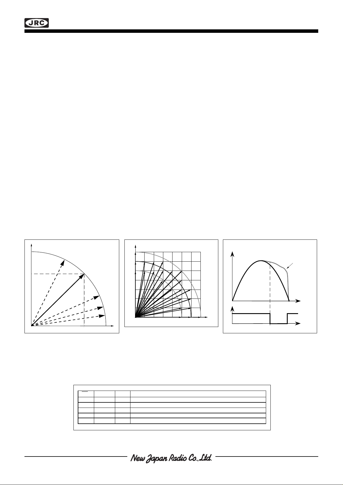
stages. This is to avoid motor current dragging which occurs at high stepping rates and during the negative current
slopes, as illustrated in figure 9. Eight different levels for initiation of fast current decay can be selected.
The sign outputs generate the phase shifts, i.e., they reverse the current direction in the phase windings.
Output
More
than 2
bits
Negative
difference
Output
Less
than 2
bits
Positive
difference
Output
Actual
Offset error
Gain
error
Correct
Endpoint
non-linearity
Input
Figure 3. Errors in D/A conversion.
Differential non-linearity of more than
1 bit, output is non-monotonic.
Input
Figure 4. Errors in D/A conversion.
Differential non-linearity of less than 1
bit, output is monotonic.
Full scale
Input
Figure 5. Errors in D/A conversion.
Non-linearity, gain and offset errors.
Page 4
NJU39610
Data Bus Interface
NJU39610 is designed to be compatible with 8-bit microprocessors such as the 6800, 6801, 6803, 6808, 6809,
8051, 8085, Z80 and other popular types and their 16/32 bit counter parts in 8 bit data mode. The data bus interface consists of 8 data bits, write signal, chip select, and two address pins. All inputs are TTL-compatible (except
reset). The two address pins control data transfer to the four internal D-type registers. Data is transferred according
to figure 10 and on the positive edge of the write signal.
Current Direction, Sign1 & Sign
2
These bits are transferred from D7 when writing in the respective DA register. A0 and A1 must be set according to
the data transfer table in figure 10.
Current Decay, CD1 & CD
2
CD1 and CD2 are two active low signals (LOW = fast current decay). CD1 is active if the previous value of DA-Data1
is strictly larger than the new value of DA-Data1 and the value of the level register LEVEL1 (L61 … L41) is strictly
larger than the new value of DA-Data1. CD1 is updated every time a new value is loaded into DA-Data1.
The logic definition of CD1 is:
CD1 = NOT{[(D6 … D0) < (Q61 … Q01)] AND[(D6 …D4) < (L61 … L41)]}
Where (D6 … D0) is the new value being sent to DA-Data1 and (Q61 … Q01) is DA-Data1’s old value. (L61 … L41) are
the three bits for setting the current decay level at LEVEL1.
The logic definition of CD2 is analog to CD1:
CD2 = NOT{[(D6 … D0) < (Q62 … Q02)] AND[(D6 …D4) < (L62 … L42)]}
Where (L62 … L42) is the level programmed in channel 2’s level register. (D6 … D0) and (Q62 … Q02) are the new and
old values of DA-Data2.
The two level registers, LEVEL1 and LEVEL2, consist of three flip flops each and they are compared against the
three most significant bits of the DA-Data value, sign bit excluded.
T [mNm]
I [mA]
2
2
T
max
T
nom
T
min
DA output [V]
Current dragging
I
I [mA]
1
Figure 6a. Assuming that torque is
proportional to the current in resp.
winding it is possible to draw figure
8b.
CS A0 A1 Data Transfer
0 0 0 D7 —> Sign1, (D6—D0) —> (Q61—Q01), New value —> CD1
0 0 1 (D6—D4) —> (L61—L41)
0 1 0 D7 —> Sign2, (D6—D0) —> (Q62—Q02), New value —> CD2
0 1 1 (D6—D4) —> (L62—L42)
1 X X No Transfer
Figure 8. Table showing how data is transfered inside NJU39610.
T [mNm]
1
Figure 6b. An example of accessible
positions with a given torque deviation/fullstep. Note that 1:st µstep
sets highest resolution. Data points
are exaggerated for illustration
purpose.
TNom = code 127.
CD
t
Time
Figure 7. Motor current dragging at
high step rates and current decay
influence. Fast current decay will
make it possible for the current to
follow the ideal sine curve. Output
shown without sign shift.
Page 5

NJU39610
DA1 and DA
2
These are the two outputs of DAC1 and DAC2. Input to the DACs are internal data bus (Q61 … Q01) and (Q62 …
Q02).
Reference Voltage V
V
is the analog input for the two DACs. Special care in layout, gives a very low voltage drop from pin to resistor.
Ref
Any V
between 0.0 V and VDD can be applied, but output might be non-linear above 3.0 V.
Ref
Ref
Power-on Reset
This function automatically resets all internal flip flops at power-on. This results in VSS voltage at both DAC outputs
and all digital outputs.
Reset
If Reset is not used, leave it disconnected. Reset can be used to measure leakage currents from VDD.
Time when motor is in
a compromise
position.
Time when micro
position is correct.
Write
signal.
Motor
position.
Writing to
channel 1.
Writing to
channel 2.
Write time = incorrect position
Useful time = correct
position
Double pulse write signal
Actual data = true position
Normal resolution
Figure 9. Double pulse programming, in- and output signals.
Time when motor is in
an intermediate
position.
Time when micro
position is almost
correct.
Write
signal.
Motor position. Note
that position is
a compromise.
Writing to
channel 1.
Writing to
channel 2.
always
Useful time = compromise position
with equally spaced angles
Useful time = almost
correct position
Single pulse write signal
"Ideal data" = desired
position
Time
Ideal data = desired position
Time
Actual data = true position
Note increased resolution
Figure 10. Single pulse programming, in- and output signals.
Page 6

NJU39610
■ ABSOLUTE MAXIMUM RATINGS
Parameter Pin no.* Symbol Min Max Unit
Voltage
Supply 5 V
Logic inputs 6- 17 V
Reference input 1 V
DD
I
R
Current
Logic inputs 6- 17 I
I
Temperature
Storage temperature T
Operating ambient temperature T
stg
opr
* refers to DIP package
■ RECOMMENDED OPERATING CONDITIONS
Parameter Symbol Min Typ Max Unit
Supply voltage V
Reference voltage ( @ VDD=5V) V
DD
R
4.75 5.0 5.25 V
0 2.5 3.8 V
- 6 V
-0.3 VDD+0.3 V
-0.3 VDD+ 0.3 V
-0.4 +0.4 mA
-55 +150 °C
-20 +85 °C
Page 7
NJU39610
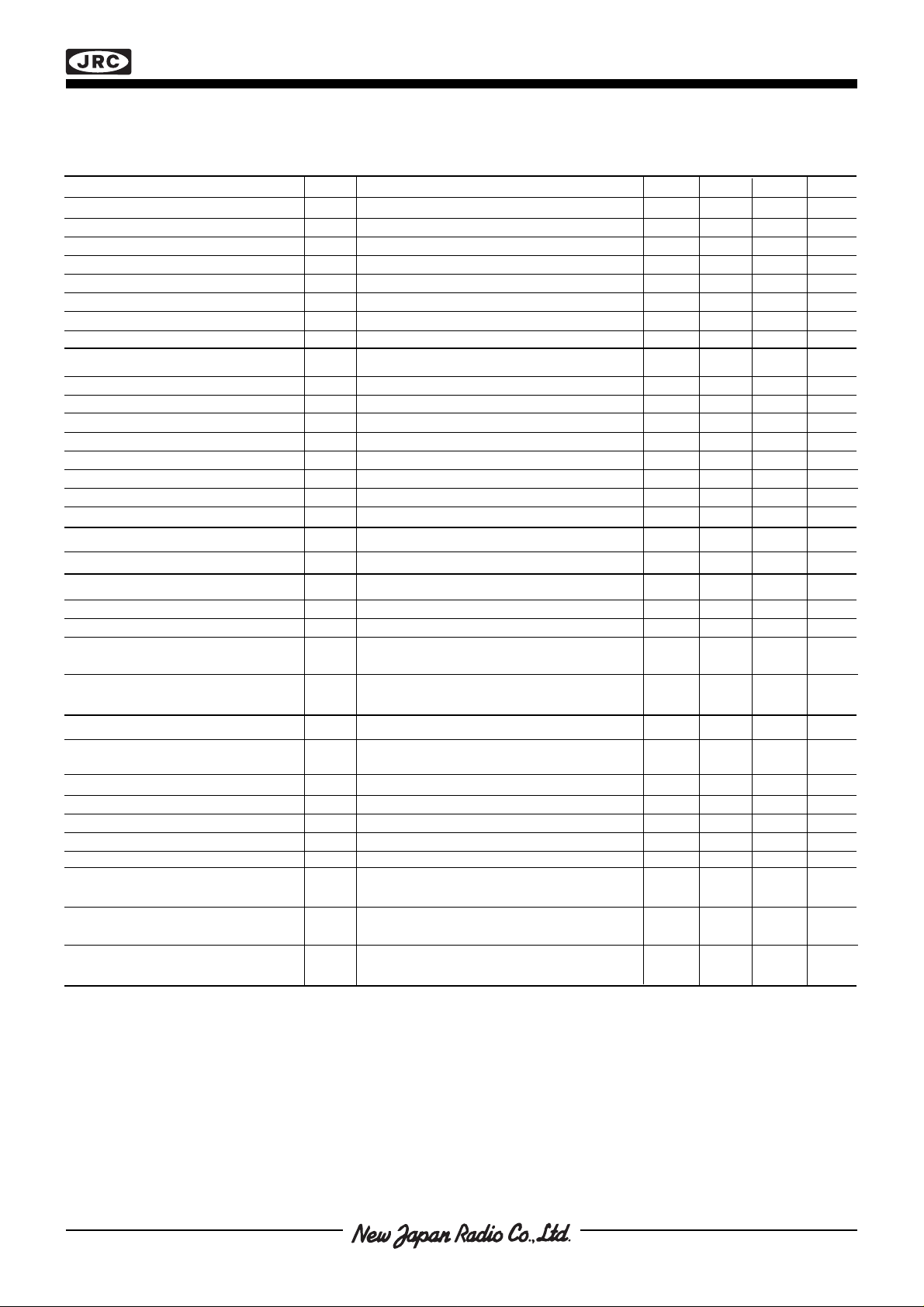
■ ELECTRICAL CHARACTERISTICS
Electrical characteristics over recommended operating conditions.
Parameter Symbol Conditions Min Typ Max Unit
Logic Inputs
Reset logic HIGH input voltage V
Reset logic LOW input voltage V
Logic HIGH input voltage V
Logic LOW input voltage V
Reset input current I
Input current, other inputs I
Input capacitance - 3 - pF
IHR
ILR
IH
IL
VSS < VIR < VDD-0.01 - 1 mA
IR
VSS < VI < VDD-1 - 1 µA
I
Internal Timing Characteristics
Address setup time t
Data setup time t
Chip select setup time t
Address hold time t
Data hold time t
Chip select hold time t
Write cycle length t
Reset cycle length t
Valid for A0, A1 60 - - ns
as
Valid for D0 - D7 60 - - ns
ds
cs
ah
dh
ch
WR
R
Reference Input
Input resistance R
Ref
Logic Outputs
Logic HIGH output current I
Logic LOW output current I
Write propagation delay t
Reset propagation delay t
DAC Outputs Reset open, V
Nominal output voltage V
VO = 2.4 V - -13 -5 mA
OH
VO = 0.4 V 1.7 5 - mA
OL
From positive edge of WR. - 30 100 ns
p
WR
outputs valid, C
From positive edge of Reset to - 60 150 ns
p
R
outputs valid, C
DA
= 120 pF
load
= 120 pF
load
= 2.5 V
Ref
Resolution - 7 - Bits
Offset error - 0.2 0.5 LSB
Gain error - 0.1 0.5 LSB
Endpoint nonlinearity - 0.2 0.5 LSB
Differential nonlinearity - 0.2 0.5 LSB
Load error (V
, unloaded - VDA, loaded) - 0.1 0.5 LSB
DA
R
= 2.5 kohm, Code 127 to DAC
load
Power supply sensitivity Code 127 to DAC - 0.1 0.3 LSB
Conversion speed t
4.75 V < V
For a full-scale transition to ±0.5 LSB - 3 8 µs
DAC
of final value, R
< 5.25 V
DD
load
= 2.5 kohm, C
= 50 pF.
load
3.5 - - V
- - 0.1 V
2.0 - - V
- - 0.8 V
70 - - ns
- - 0 ns
- - 0 ns
- - 0 ns
50 - - ns
80 - - ns
6 9 - kohm
0 -V
Ref
-1LSB V
Page 8
NJU39610
CS
A0-A1
D0-D7
WR
DA
Sign, CD
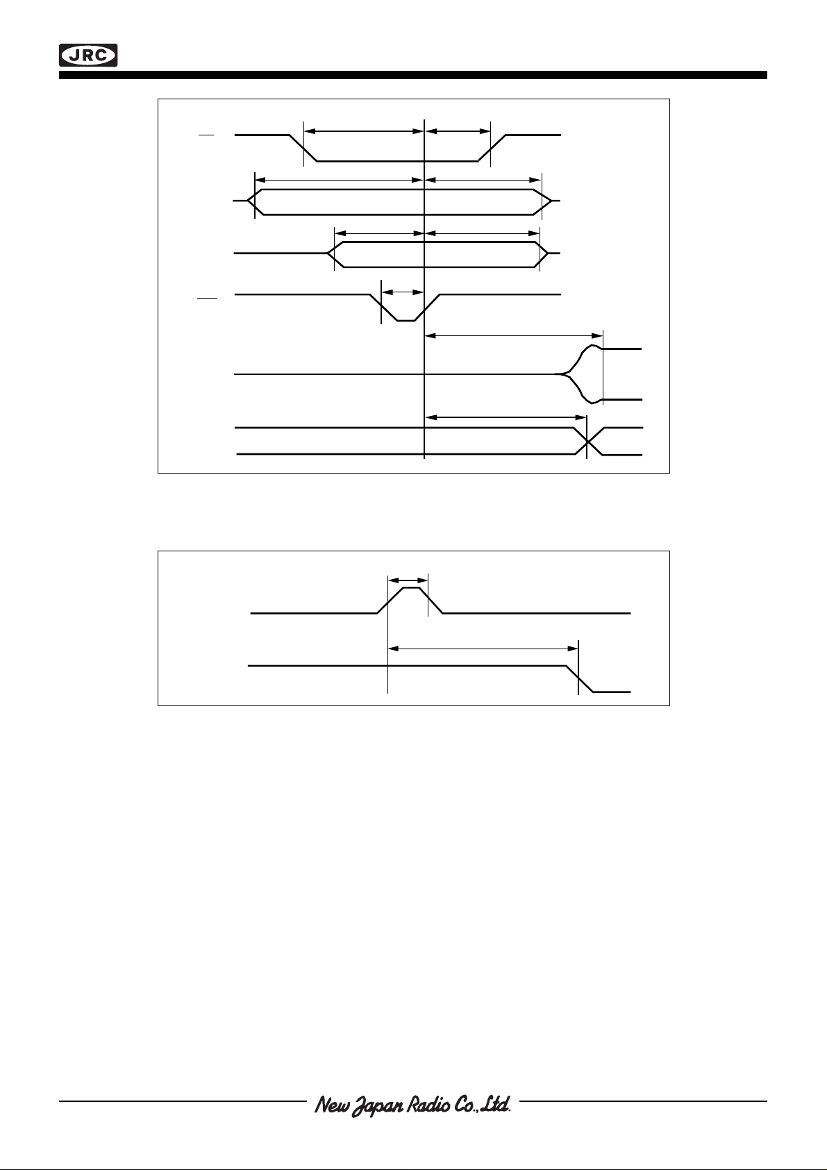
Figure 11. Timing
cs
t
as ah
t
ds
t
WR
tt
ch
t
t
dh
t
DAC
t
pwr
Reset
Sign, CD
Figure 12. Timing of Reset
t
res
t
pres
Page 9

NJU39610
■ APPLICATIONS INFORMATION
How Many Microsteps?
The number of true microsteps that can be obtained depends upon many different variables, such as the number of
data bits in the Digital-to-Analog converter, errors in the converter, acceptable torque ripple, single- or double-pulse
programming, the motor’s electrical, mechanical and magnetic characteristics, etc. Many limits can be found in the
motor’s ability to perform properly; overcome friction, repeatability, torque linearity, etc. It is important to realize that
the number of current levels, 128 (27), is
(reference voltage levels) available from each driver stage. Combining a current level in one winding with any of
128 other current levels in the other winding will make up 128 current levels. So expanding this, it is possible to get
16,384 (128 • 128) combinations of different current levels in the two windings. Remember that these 16,384 micropositions are not all useful, the torque will vary from 100% to 0% and some of the options will make up the same
position. For instance, if the current level in one winding is OFF (0%) you can still vary the current in the other
winding in 128 levels. All of these combinations will give you the same position
Typical Application
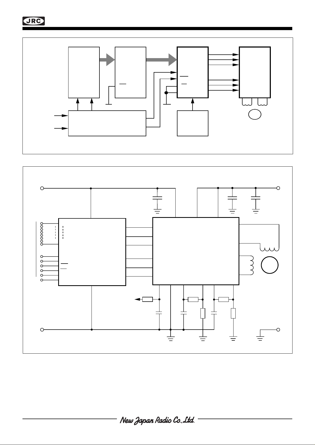
The microstepper solution can be used in a system with or without a micro-processor.
Without a microprocessor, a counter addresses a ROM where appropriate step data is stored. Step and Direction
are the input signals which represent clock and up / down of counter. This is the ideal solution for a system where
there is no microprocessor or it is heavily loaded with other tasks.
With a microprocessor, data is stored in ROM / RAM area or each step is successively calculated. NJU39610 is
connected like any peripheral addressable device. All parts of stepping can be tailored for specific damping needs
etc. This is the ideal solution for a system where there is an available microprocessor with extra capacity and low
cost is more essential than simplicity. See typical application, figure 14.
not
the number of steps available. 128 is the number of current levels
but
a varying torque.
■ User Hints
Never disconnect ICs or PC Boards when power is supplied.
Choose a motor that is rated for the current you need to establish desired torque. A high supply voltage will gain
better stepping performance even if the motor is not rated for the VMM voltage, the current regulation in NJM3771
will take care of it. A normal stepper motor might give satisfactory result, but while microstepping, a “microsteppingadapted” motor is recommended. This type of motor has smoother motion due to two major differences, the stator /
rotor teeth relationship is non-equal and the static torque is lower.
The NJU39610 can handle programs which generate microsteps at a desired resolution as well as quarter
stepping, half stepping, full stepping, and wave drive.
Fast or Slow Current Decay?
There is a difference between static and dynamic operation of which the actual application must decide upon when
to use fast or slow current decay. Generally slow decay is used when stepping at slow speeds. This will give the
benefits of low current ripple in the drive stage, a precise and high overall average current, and normal current
increase on the positive edge of the sine-cosine curves. Fast current decay is used at higher speeds to avoid
current dragging with lost positions and incorrect step angles as a result.
Ramping
Every drive system has inertia which must be considered in the drive system. The rotor and load inertia play a big
role at higher speeds. Unlike the DC motor, the stepper motor is a synchronous motor and does not change its
speed due to load variations. Examining a typical stepper motor’s torque-versus-speed curve indicates a sharp
torque drop-off for the “start-stop without error” curve. The reason for this is that the torque requirements increase
by the cube of the speed change. For good motor performance, controlled acceleration and deceleration should be
considered even though microstepping will improve overall performance.
Page 10

NJU39610
■ Programming NJU39610
There are basically two different ways of programming the NJU39610. They are called “single-pulse programming”
and “double-pulse programming.” Writing to the device can only be accomplished by addressing one register at a
time. When taking one step, at least two registers are normally updated. Accordingly there must be a certain time
delay between writing to the first and the second register. This programming necessity gives some special stepping
advantages.
Double-pulse Programming
The normal way is to send two write pulses to the device, with the correct addressing in between, keeping the delay
between the pulses as short as possible. Write signals will look as illustrated in figure9. The advantages are:
• low torque ripple
• correct step angles between each set of double pulses
• short compromise position between the two step pulses
• normal microstep resolution
Single-pulse Programming
A different approach is to send one pulse at a time with an equally-spaced duty cycle. This can easily be accomplished and any two adjacent data will make up a microstep position. Write signals will look as in figure 10. The
advantages are:
• higher microstep resolution
• smoother motion
The disadvantages are:
• higher torque ripple
• compromise positions with almost-correct step angles
Page 11
NJU39610
Counter PROM
D0-D7
NJU39610 NJM3771
A0
WR
CE
Clock Up/Dn
CS
A1 Vref
Step
Voltage
Reference
Direction
Control Logic
Figure 13. Typical blockdiagram of an application without a microprocessor.
V (+5 V)
CC
0.1 µF 0.1 µF
+
10 µF
V
MM
5
To
µP
+2.5V
14
D0
7
D7
15
A0
16
A1
6
WR
17
CS
22
RESET
1
VV
Ref
GND
(V )
CC MM
V
DD
NJU39610
SS
18
Sign
CD
DA
Sign
CD
DA
3
1
4
1
2
1
20
2
19
2
21
2
+5 V
7
8
9
16
15
14
15 kΩ
3 300 pF
Phase
CD
V
Phase
CD
V
RC
12
1
1
R1
2
2
R2
5, 6,
17, 18
Figure 14. Typical application in a microprocessor based system.
11 3 20
V
CC
VV
MM1 MM2
NJM3771
11
2
10
1 kΩ 1 kΩ
820 pF 820 pF
1.0 Ω 1.0 Ω
R
13
4
M
A1
M
1
B1
19
M
A2
22
M
B2
21
ECECGND
2
2
STEPPER
MOTOR
Pin numbers refer
to DIP package.
R
S
S
GND (V
)
The specifications on this databook are only
given for information , without any guarantee
as regards either mistakes or omissions. The
application circuits in this databook are
described only to show representative usages
of the product and not intended for the
guarantee or permission of any right including
the industrial rights.
 Loading...