

Page 1
DUAL STEPPER MOTOR DRIVER
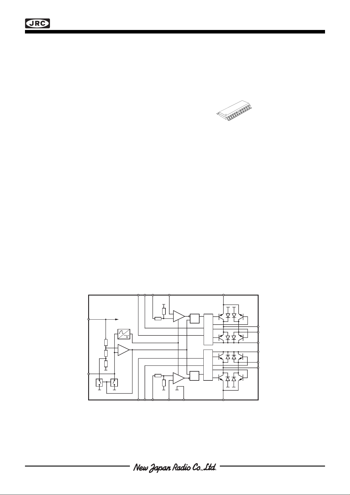
■ GENERAL DESCRIPTION ■ PACKAGE OUTLINE
The NJM3777 is a switch-mode (chopper), constant-current
driver with two channels: one for each winding of a two-phase
stepper motor. The NJM3777 is equipped with a Disable input
to simplify half-stepping operation. The NJM3777 contains a
clock oscillator, which is common for both driver channels, a
set of comparators and flip-flops implementing the switching
control, and two output H-bridges, including recirculation
diodes. Voltage supply requirements are + 5 V for logic and +
10 to + 45 V for the motor. Maximum output current is 900mA
per channel.
■ FEATURES
• Dual chopper driver
• 900 mA continuous output current per channel
NJM3777E3
NJM3777
• Digital filter on chip eliminates external filtering components
• Package EMP24(Batwing)
■ BLOCK DIAGRAM
C
V
Dis
1
1
R1
–
+
+
–
V
RC
CC
NJM3777
Phase
1
V
CC
+
–
R
S
SRQ
E
1
Q
M
A1
Logic
Logic
M
B1
V
MM1
V
MM2
M
B2
M
A2
Figure 1. Block diagram
Phase
Dis
V
2
2
R2
GNDC
2
E
2
Page 2
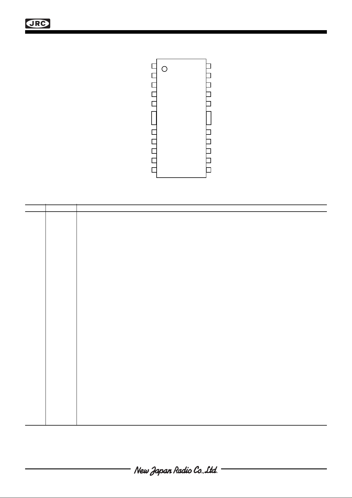
■ PIN CONFIGURATION
Figure 2. Pin configuration
■ PIN DESCRIPTION
NC
MB
MA
VMM
GND
GND
VR
Phase
Dis
RC
NJM3777
1
2
1
E
3
1
4
1
5
1
6
7
8
1
9
C
1
10
1
11
1
NJM
3777E3
24
23
22
21
20
19
18
17
16
15
14
1312
NC
MB
2
E
2
MA
2
VMM
GND
GND
VR
2
C
2
Phase
Dis
2
V
cc
2
2
EMP Symbol Description
1 NC Not connected
2M
3E
4M
5V
B1
1
A1
MM1
Motor output B, channel 1. Motor current flows from MA1 to MB1 when Phase1 is HIGH.
Common emitter, channel 1. This pin connects to a sensing resistor RS to ground.
Motor output A, channel 1. Motor current flows from MA1 to MB1 when Phase1 is HIGH.
Motor supply voltage, channel 1, +10 to +40 V. V
MM1
and V
should be connected together.
MM2
6, 7, GND Ground and negative supply. Note: these pins are used thermally for heat-sinking.
18, 19 Make sure that all ground pins are soldered onto a suitably large copper ground plane for efficient heat -
sinking.
8V
9C
R1
1
Reference voltage, channel 1. Controls the comparator threshold voltage and hence the output current.
Comparator input channel 1. This input senses the instantaneous voltage across the sensing resistor,
filtered by the internal digital filter or an optional external RC network.
10 Phase
11 Dis
Controls the direction of motor current at outputs MA1 and MB1. Motor current flows from MA1 to MB1 when
1
Phase
is HIGH.
1
Disable input for channel 1. When HIGH, all four output transistors are turned off, which results in a
1
rapidly decreasing output current to zero.
12 RC Clock oscillator RC pin. Connect a 12 kohm resistor to V
and a 4 700 pF capacitor to ground to obtain
CC
the nominal switching frequency of 23.0 kHz and a digital filter blanking time of 1.0 µs.
13 V
14 Dis
CC
Logic voltage supply, nominally +5 V.
Disable input for channel 2. When HIGH, all four output transistors are turned off, which results in a
2
rapidly decreasing output current to zero.
15 Phase
16 C
2
Controls the direction of motor current at outputs MA2 and MB2. Motor current flows from MA2 to MB2 when
2
Phase
is HIGH.
2
Comparator input channel 2. This input senses the instantaneous voltage across the sensing resistor,
filtered by the internal digital filter or an optional external RC network.
17 V
20 V
21 M
22 E
23 M
R2
MM2
A2
2
B2
Reference voltage, channel 2. Controls the comparator threshold voltage and hence the output current.
Motor supply voltage, channel 2, +10 to +40 V. V
MM1
and V
should be connected together.
MM2
Motor output A, channel 2. Motor current flows from MA2 to MB2 when Phase2 is HIGH.
Common emitter, channel 2. This pin connects to a sensing resistor RS to ground.
Motor output B, channel 2. Motor current flows from MA2 to MB2 when Phase2 is HIGH.
24 NC Not connected
Page 3
NJM3777
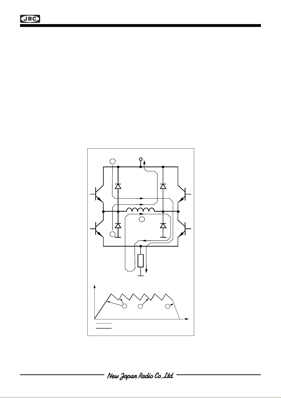
■ FUNCTIONAL DESCRIPTION
Each channel of the NJM3777 consists of the following sections: an output H-bridge with four transistors and four
recirculation diodes, capable of driving up to 800 mA continuous current to the motor winding, a logic section that
controls the output transistors, an S-R flip-flop, and a comparator. The clock-oscillator is common to both channels.
Constant current control is achieved by switching the output current to the windings. This is done by sensing the
peak current through the winding via a current-sensing resistor RS, effectively connected in series with the motor
winding. As the current increases, a voltage develops across the sensing resistor, which is fed back to the comparator. At the predetermined level, defined by the voltage at the reference input VR, the comparator resets the flipflop, which turns off the upper output transistor. The turn-off of one channel is independent of the other channel.
The current decreases until the clock oscillator triggers the flip-flops of both channels simultaneously, which turns
on the output transistors again, and the cycle is repeated.
To prevent erroneous switching due to switching transients at turn-on, the NJM3777 includes a digital filter. The
clock oscillator provides a blanking pulse which is used for digital filtering of the voltage transient across the
current sensing resistor during turn-on.
The current paths during turn-on, turn-off and phase shift are shown in figure 3.
V
MM
1
2
3
R
S
Motor Current
1 2
Fast Current Decay
Slow Current Decay
3
Figure 3. Output stage with current paths
during turn-on, turn-off and phase shift.
Time
Page 4

NJM3777
■ ABSOLUTE MAXIMUM RATINGS
Parameter Pin No. Symbol Min Max Unit
Voltage
Logic supply 13 V
Motor supply 5, 20 V
Logic inputs 10, 11, 14, 15 V
Analog inputs 8, 9, 16, 17 V
Current
Motor output current 2, 4, 21, 23 I
Logic inputs 10, 11, 14, 15 I
Analog inputs 8, 9, 16, 17 I
Temperature
Operating junction temperature T
Storage temperature T
Power Dissipation (Package Data)
Power dissipation at T
Power dissipation at T
= +25°CP
GND
= +125°CP
GND
■ RECOMMENDED OPERATING CONDITIONS
CC
MM
I
A
M
I
A
J
S
D
D
07V
045V
-0.3 6 V
-0.3 V
CC
V
-900 +900 mA
-10 - mA
-10 - mA
-40 +150 °C
-55 +150 °C
-5W
-2W
Parameter Symbol Min Typ Max Unit
Logic supply voltage V
Motor supply voltage V
Output emitter voltage V
Motor output current I
Operating junction temperature T
Rise and fall time logic inputs t
Oscillator timing resistor R
C
V
Phase
Dis
1
R1
1
1
8
NJM3777
V
I
CC
CC
13
12 kΩ
R
T
I
RC
RC
12
4 700 pF
V
CC
C
T
I I I
I IH IL
I
I
A
V
I
V
V
A
IH
V
V
R
IL
R
V
RC
10
V
CC
+
–
15
Phase
2
9
11
–
R
Q
+
S
SRQ
+
–
6, 7, 18, 19
16
17
14
Dis
V
2
R2
GNDC
2
I
C
I
A
V
CH
V
C
V
A
E
1
3
M
4
A1
Logic
Logic
22
E
2
R
S
M
2
B1
V
5
MM1
I
V
MM
MM2
20
M
23
B2
I I
M OL
M
A2
21
V
V
E
M
V
MA
CC
MM
E
M
J
, t
r,
f
T
V
MM
4.75 5 5.25 V
10 - 40 V
- - 1.0 V
-800 - +800 mA
-20 - +125 °C
--2µs
21220kΩ
| V – V |
MA MB
50 %
V
CH
V ( I )
E M
V
RC
f =
s
t
tont
1
+
t
on
off
t
d
t
b
t
on
D =
+
off
tt
on
off
t
t
t
Figure 5. Definition of termsFigure 4. Definition of symbols
Page 5

NJM3777
■ ELECTRICAL CHARACTERISTICS
Electrical characteristics over recommended operating conditions, unless otherwise noted. - 20°C ≤ Tj ≤ + 125°C.
Parameter Symbol Conditions Min Typ Max Unit
General
Supply current I
Supply current I
Total power dissipation P
Total power dissipation P
Thermal shutdown junction temperature - 160 - °C
Turn-off delay t
Logic Inputs
Logic HIGH input voltage V
Logic LOW input voltage V
Logic HIGH input current I
Logic LOW input current I
Analog Inputs
Threshold voltage V
Input current I
|V
| mismatch V
C1—VC2
Motor Outputs
Lower transistor saturation voltage I
Lower transistor leakage current V
Lower diode forward voltage drop I
Upper transistor saturation voltage I
Upper transistor leakage current V
Upper diode forward voltage drop I
Chopper Oscillator
Chopping frequency f
Digital filter blanking time t
Note 4. - 85 99 mA
CC
Dis1= Dis2= HIGH. - 7 10 mA
CC
VMM= 24 V, IM1= IM2= 650 mA. - 2.9 3.4 W
D
Notes 2, 3, 4.
VMM= 24 V, IM1= 800 mA, IM2= 0 mA. - 2.3 2.7 W
D
Notes 2, 3, 4.
dVC/dt ≥ 50 mV/µs, - 1.1 2.0 µs
d
I
= 100 mA. Note 3.
M
IH
IL
VI = 2.4 V - - 20 µA
IH
VI = 0.4 V -0.2 -0.1 - mA
IL
VR= 5 V 480 500 520 mV
CH
VR= 5 V - 500 - µA
A
Cdiff
= 500 mA - 0.5 0.8 V
M
=41 V,Dis1= Dis2= HIGH. - - 50 µA
MM
= 500 mA - 1.2 1.3 V
M
= 500 mA. - 1.4 1.6 V
M
=41 V, Dis1= Dis2= HIGH. - - 50 µA
MM
= 500 mA. - 1.3 1.5 V
M
CT = 4 700 pF, RT = 12 kohm 21.5 23.0 24.5 kHz
s
CT = 4 700 pF. Note 3. - 1.0 - µs
b
2.0 - - V
- - 0.6 V
-520mV
■ THERMAL CHARACTERISTICS
Parameter Symbol Conditions Min Typ Max Unit
Thermal resistance Rth
Rth
J-GND
Note 2. - 42 - °C/W
J-A
Notes
1. All voltages are with respect to ground. Currents are positive into, negative out of specified terminal.
2. All ground pins soldered onto a 20 cm2 PCB copper area with free air convection, TA = + 25° C.
3. Not covered by final test program.
4. Switching duty cycle D = 30 %, f
= 23.0 kHz.
s
-13-°C/W
Page 6

NJM3777
■ APPLICATIONS INFORMATION
Current control
The regulated output current level to the motor winding is determined by the voltage at the reference input and the
value of the sensing resistor, RS. The peak current through the sensing resistor (and the motor winding) can be
expressed as:
I
= 0.1•VR / RS[A]
M,peak
With a recommended value of 0.5 ohm for the sensing resistor RS, a 2.5 V reference voltage will produce an output
current of approximately 500 mA. RS should be selected for maximum motor current. Be sure not to exceed the
absolute maximum output current which is 900 mA. Chopping frequency, winding inductance and supply voltage
also affect the current, but to much less extent.
For accurate current regulation, the sensing resistor should be a 0.5 - 1.0 W precision resistor, i. e. less than 1%
tolerance and low temperature coefficient.
+5 V
+5 V
10
11
15
14
17
12 kΩ
8
Phase
Dis
V
Phase
Dis
V
RC
12
0.1 µF
1
R1
2
R2
13 5 20
V
CC
1
VV
NJM3777E3
2
112 2
6, 7,
18, 19
9
MM1 MM2
M
M
M
M
316 22
4
A1
2
B1
21
A2
23
B2
ECECGND
V
MM
+
10 µF0.1 µF
STEPPER
MOTOR
4 700 pF
R
S
0.47 Ω
GND (V ) GND (V
CC
R
0.47 Ω
S
Pin numbers refer
to EMP package.
Figure 6. Typical stepper motor driver application with NJM3777
V (+5 V)
CC
0.1 F 0.1 F
Phase
Dis
1
V
R1
Phase
Dis
V
R2
RC
2
6, 7,
18, 19
V
CC
1
NJM3777E3
2
13 5 20
VV
MM1 MM2
1122
3
16
9
0.47 ‰ 0.47 ‰
R
S
4
M
A1
M
2
B1
21
M
A2
23
M
B2
ECECGND
22
R
S
13
D0
6
To
P
+2.5V
D7
14
A0
5
WR
16
CS
20
RESET
1
VV
Ref
GND
(V )
CC MM
4
V
DD
NJU39612E2
SS
17
Sign
Sign
1
DA
1
2
DA
2
11
8
2
15
18
14
17
19
12
12 k‰
+5 V
4700 pF
10
3
)
MM
V
MM
+
10 F
STEPPER
MOTOR
Pin numbers refer
to EMP package.
GND (V
)
Figure 7. Typical microstepping application with NJU39612
Page 7

NJM3777
Current sense filtering
At turn-on a current spike occurs, due to the recovery of the recirculation diodes and the capacitance of the motor
winding. To prevent this spike from reseting the flip-flops through the current sensing comparators, the clock
oscillator generates a blanking pulse at turn-on. The blanking pulse pulse disables the comparators for a short time.
Thereby any voltage transient across the sensing resistor will be ignored during the blanking time.
Choose the blanking pulse time to be longer than the duration of the switching transients by selecting a proper C
value. The time is calculated as:
tb = 210 • CT[s]
As the CT value may vary from approximately 2 200 pF to 33 000 pF, a blanking time ranging from 0.5 µs to 7 µs is
possible. Nominal value is 4 700 pF, which gives a blanking time of 1.0 µs.
As the filtering action introduces a small delay, the peak value across the sensing resistor, and hence the peak
motor current, will reach a slightly higher level than what is defined by the reference voltage. The filtering delay also
limits the minimum possible output current. As the output will be on for a short time each cycle, equal to the digital
filtering blanking time plus additional internal delays, an amount of current will flow through the winding. Typically
this current is 1-10 % of the maximum output current set by RS.
When optimizing low current performance, the filtering may be done by adding an external low pass filter in series
with the comparator C input. In this case the digital blanking time should be as short as possible. The recommended filter component values are 1 kohm and 820 pF. Lowering the switching fre- quency also helps reducing
the minimum output current.
To create an absolute zero current, the Dis input should be HIGH.
Switching frequency
The frequency of the clock oscillator is set by the timing components RT and CT at the RC-pin. As CT sets the digital
filter blanking time, the clock oscillator frequency is adjusted by RT. The value of RT is limited to 2 - 20 kohm. The
frequency is approximately calculated as:
fs = 1 / ( 0.77 • RT • CT)
Nominal component values of 12 kohm and 4 700 pF results in a clock frequency of 23.0 kHz. A lower frequency
will result in higher current ripple, but may improve low level linearity. A higher clock frequency reduces current
ripple, but increases the switching losses in the IC and possibly the iron losses in the motor.
T
Phase inputs
A logic HIGH on a Phase input gives a current flowing from pin MA into pin MB.
A logic LOW gives a current flow in the opposite direction. A time delay prevents cross conduction in the H-bridge
when changing the Phase input.
Phase
1
Dis
1
Phase
2
Dis
2
V
R1
Thermal resistance [°C/W]
80
70
60
50
40
30
20
5101520
PCB copper foil area [cm ]
EMP package
24-pin
EMP
30 3525
2
140%
100%
V
140%
100%
I
140%
100%
–100%
–140%
I
140%
100%
–100%
–140%
R2
MA1
MA2
Full step mode Half step mode Modified half step mode
Figure 8. Typical thermal resistance vs. PC Board
copper area and suggested layout
Figure 9. Stepping modes
Page 8

NJM3777
Dis (Disable) inputs
A logic HIGH on the Dis inputs will turn off all four transistors of the output H-bridge, which results in a rapidly
decreasing out- put current to zero.
VR (Reference) inputs
The Vref inputs of the NJM3777 have a voltage divider with a ratio of 1 to 10 to reduce the external reference
voltage to an adequate level. The divider consists of closely matched resistors. Nominal input reference voltage is 5
V.
Interference
Due to the switching operation of NJM3777, noise and transients are generated and might be coupled into adjacent
circuitry. To reduce potential interference there are a few basic rules to follow:
• Use separate ground leads for power ground (the ground connection of RS), the ground leads of NJM3777, and
the ground of external analog and digital circuitry. The grounds should be connected together close to the GND
pins of NJM3777.
• Decouple the supply voltages close to the NJM3777 circuit. Use a ceramic capacitor in parallel with an electrolytic
type for both VCC and VMM. Route the power supply lines close together.
• Do not place sensitive circuits close to the driver. Avoid physical current loops, and place the driver close to both
the motor and the power supply connector. The motor leads could preferably be twisted or shielded.
Motor selection
The NJM3777 is designed for two-phase bipolar stepper motors, i.e. motors that have only one winding per phase.
The chopping principle of the NJM3777 is based on a constant frequency and a varying duty cycle. This scheme
imposes certain restrictions on motor selection. Unstable chopping can occur if the chopping duty cycle exceeds
approximately 50 %. See figure 5 for definitions. To avoid this, it is necessary to choose a motor with a low winding
resistance and inductance, i.e. windings with a few turns.
It is not possible to use a motor that is rated for the same voltage as the actual supply voltage. Only rated current
needs to be considered. Typical motors to be used together with the NJM3777 have a voltage rating of 1 to 6 V,
while the supply voltage usually ranges from 10 to 40 V.
Low inductance, especially in combination with a high supply voltage, enables high stepping rates. However, to
give the same torque capability at low speed, the reduced number of turns in the winding in the low resistive, low
inductive motor must be compensated by a higher current. A compromise has to be made. Choose a motor with the
lowest possible winding resistance and inductance, that still gives the required torque, and use as high supply
voltage as possible, without exceeding the maximum recommended 40 V. Check that the chopping duty cycle does
not exceed 50 % at maximum current.
Heat sinking
NJM3777 is a power IC, packaged in a power EMP package. The ground leads of the package (the batwing) are
thermally connected to the chip. External heatsinking is achieved by soldering the ground leads onto a copper
ground plane on the PCB.
Maximum continuous output current is heavily dependent on the heatsinking and ambient temperature. Consult
figures 8, 10 and 11to determine the necessary heat- sink, or to find the maximum output current under varying
conditions.
A copper area of 20 cm2 (approx. 1.8” x 1.8”), copper foil thickness 35 µm on a 1.6 mm epoxy PCB, permits the
circuit to operate at 2 x 450 mA output current, at ambient temperatures up to 85° C.
Thermal shutdown
The circuit is equipped with a thermal shutdown function that turns the outputs off at a chip (junction) temperature
above 160° C. Normal operation is resumed when the temperature has decreased.
Programming
Figure 9 shows the different input and output sequences for full-step, half-step and modified halfstep operations.
Page 9

NJM3777
Full-step mode
Both windings are energized at all the time with the same current, IM1 = IM2. To make the motor take one step, the
current direction (and the magnetic field direction) in one phase is reversed. The next step is then taken when the
other phase current reverses. The current changes go through a sequence of four different states which equal four
full steps until the initial state is reached again.
Half-step mode
In the half-step mode, the current in one winding is brought to zero before a complete current reversal is made. The
motor will then have taken two half steps equalling one full step in rotary movement. The cycle is repeated, but on
the other phase. A total of eight states are sequenced until the initial state is reached again.
Half-step mode can overcome potential resonance problems. Resonances appear as a sudden loss of torque at
one or more distinct stepping rates and must be avoided so as not to loose control of the motor´s shaft position.
One disadvantage with the half-step mode is the reduced torque in the half step positions, in which current flows
through one winding only. The torque in this position is approximately 70 % of the full step position torque.
Modified half-step mode
The torque variations in half step mode will be elimi-nated if the current is increased about 1.4 times in the halfstep
position. A constant torque will further reduce resonances and mechanical noise, resulting in better performance,
life expectancy and reliability of the mechanical system.
Modifying the current levels must be done by bringing the reference voltage up (or down) from its nominal value
correspondingly. This can be done by using DACs or simple resistor divider networks. The NJM3777 is designed to
handle about 1.4 times higher current in one channel on mode, for example 2 x 600 mA in the full-step position,
and 1 x 800 mA in the half-step position.
Page 10

■ TYPICAL CHARACTERISTICS
NJM3777
PD (W)
3.0
2.0
Two channels on
1.0
One channel on
0
0 0.20 0.40 0.60 0.80
(A)
I
M
Figure 10. Power dissipation vs.
motor current.Ta = 25°C
V
(V)
d, ld
1.2
1.0
0.8
Maximum allowable power dissipation [W]
6
5
A
m
4
3
2
1
0
-25
b
ie
n
t te
m
p
e
ra
tu
re
0 25 50 75 125 150
Temperature [°C]
EMP package All ground pins soldered onto a
20 cm PCB copper area with
free air convection.
Batwing pin temperature
100
2
Figure 11. Maximum allowable power
dissipation
V
(V)
CE Sat
1.2
1.0
0.8
V
(V)
CE Sat
1.2
1.0
0.8
0.6
0.4
0.2
0
0 0.20 0.40 0.60 0.80
I
(A)
M
Figure 12. Typical lower transistor
saturation voltage vs. output current
(V)
V
d, ud
1.2
1.0
0.8
0.6
0.4
0.2
0
0 0.20 0.40 0.60 0.80
I
(A)
M
Figure 13. Typical lower diode
voltage drop vs. recirculating
current
0.6
0.4
0.2
0
0 0.20 0.40 0.60 0.80
I
(A)
M
Figure 14. Typical upper transistor
saturation voltage vs. output current
0.6
0.4
0.2
0
0 0.20 0.40 0.60 0.80
(A)
I
M
Figure 15. Typical upper diode
voltage drop vs. recirculating current
The specifications on this databook are only
given for information , without any guarantee
as regards either mistakes or omissions.
The application circuits in this databook are
described only to show representative
usages of the product and not intended for
the guarantee or permission of any right
including the industrial rights.
 Loading...