

Page 1
NJM3774
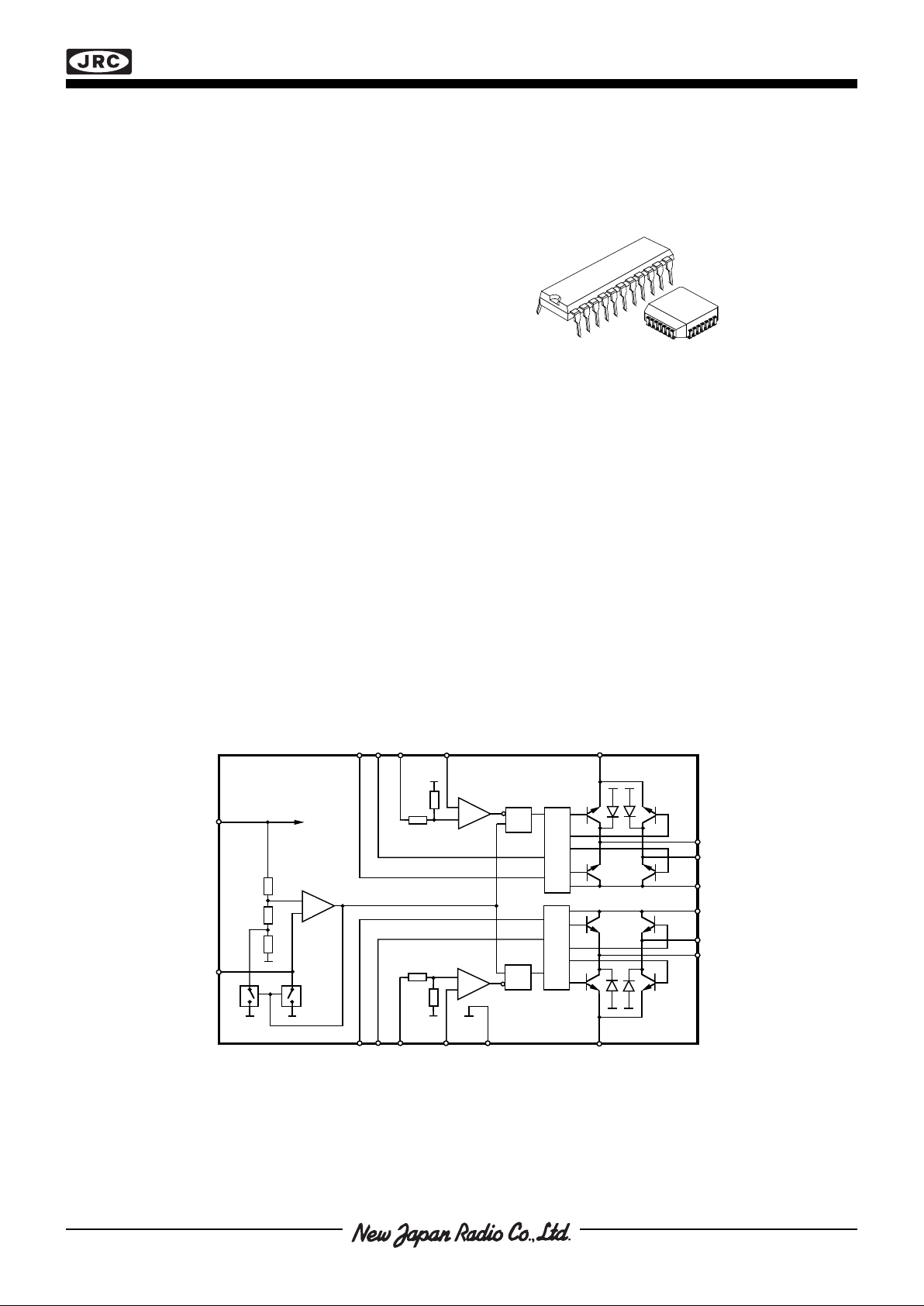
Figure 1. Block diagram
DUAL STEPPER MOTOR DRIVER
■ GENERAL DESCRIPTION ■ PACKAGE OUTLINE
RC
NJM3774
M
A1
M
B1
M
B2
M
A2
GNDC
2
V
R2
Phase
2
V
CC
C
1
V
R1
Phase
1
E
1
E
2
V
CC
SRQ
+
–
Logic
S
R
Q
+
–
Logic
+
–
V
MM2
V
MM1
Dis
1
Dis
2
NJM3774FM2
NJM3774D2
The NJM3774 is a switch-mode (chopper), constantcurrent driver with two channels: one for each winding of a
two-phase stepper motor. The NJM3774 is equipped with a
TTL level compatible Disable input to simplify half-stepping
operation. The circuit is well suited for microstepping
applications together with the matching dual DAC
NJU39610. In full/half stepping applications, the NJM3517
can be used as a phase generator (translator) to derive the
necessary signals for the NJM3774. The NJM3774 contains a clock oscillator, which is common for both driver
channels, a set of comparators and flip-flops implementing
the switching control, and two output H-bridges. Voltage
supply requirements are +5 V for logic and +10 to +45 V for
the motor. Maximum output current is 1000mA per channel.
■ FEATURES
• Dual chopper driver
• 1000 mA continuous output current per channel
• Specially matched to the Dual DAC NJU39610
• Packages DIP22 / PLCC28
■ BLOCK DIAGRAM
Page 2
NJM3774
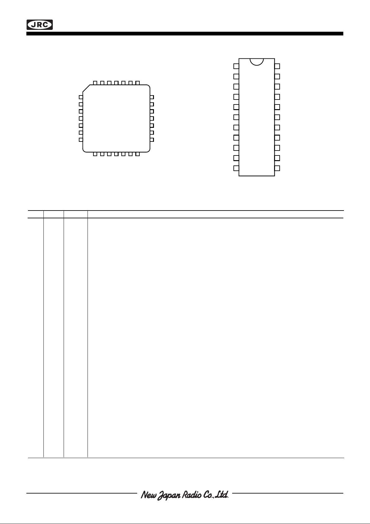
Figure 2. Pin configurations
C
E
B2
B1
GND
C
RC
V
M
GND
GND
GND
GND
A1
GND
GND
GND
GND
GND
5
6
7
8
9
10
11
25
24
23
22
21
20
19
4
3
2
1
282726
12131415161718
V
R2
V
R1
CC
Phase
2
A2
2
Dis
M
M
1
Dis
M
1
Phase
2
1
2
V
MM1
E
1
V
MM2
NJM3774FM2
1
2
3
4
5
6
7
8
9
10
11
22
21
20
19
18
17
16
15
14
13
12
C
R2
A1
GND
GND
1
R1
CC
M
V
M
GND
GND
Phase
Dis
RC
V
M
Phase
V
V
2
2
A2
MM2
B2
2
E
2
C
1
Dis
1
V
MM1
M
B1
E
1
NJM
3774D2
■ PIN CONFIGURATIONS
■ PIN DESCRIPTION
PLCC DIP Symbol Description
1-3, 9, 5, 6 GND Ground and negative supply. Note: these pins are used thermally for heat-sinking. Make sure that all
13-17 17, 18 ground pins are soldered onto a suitably large copper ground plane for efficient heat sinking.
28
48MA2Motor output A, channel 2. Motor current flows from MA2 to MB2 when Phase2 is HIGH.
59V
MM2
Motor supply voltage, channel 2, +10 to +40 V.V
MM1
and V
MM2
should be connected together.
610E2Common emitter, channel 2. This pin connects to a sensing resistor RS to ground.
711M
B2
Motor output B, channel 2. Motor current flows from MA2 to MB2 when Phase2 is HIGH.
812M
B1
Motor output B, channel 1. Motor current flows from MA1 to MB1 when Phase1 is HIGH.
10 13 E
1
Common emitter, channel 1. This pin connects to a sensing resistor RS to ground.
11 14 V
MM1
Motor supply voltage, channel 1, +10 to +40 V. V
MM1
and V
MM2
should be connected together.
12 15 M
A1
Motor output A, channel 1. Motor current flows from MA1 to MB1 when Phase1 is HIGH.
18 16 Dis
1
Disable input (TTL level compatible) for channel 1. When HIGH, all four output transistors are turned
off, which results in a rapidly decreasing output current to zero.
19 19 Phase
1
Controls the direction of motor current at outputs MA1 and MB1. Motor current flows from MA1 to M
B1
when Phase1 is HIGH.
20 20 V
R1
Ref. voltage, channel 1. Controls the threshold voltage for the comparator and hence the output
current.
21 21 C
1
Comparator input channel 1. This input senses the instantaneous voltage across the sensing resistor,
filtered by an RC network. The threshold voltage for the comparator is V
CH1
= 0.18 • VR1 [V], i.e. 450
mV at VR1 = 2.5 V.
22 22 V
CC
Logic voltage supply, nominally +5 V.
23 1 RC Clock oscillator RC pin. Connect a 15 kohm resistor to V
CC
and a 3300 pF capacitor to ground to obtain
the nominal switching frequency of 26.5 kHz.
24 2 C
2
Comparator input channel 2. This input senses the instantaneous voltage across the sensing resistor,
filtered by an RC network. The threshold voltage for the comparator is V
CH2
= 0.18 • VR2 [V], i.e. 450 mV
at VR2 = 2.5 V.
25 3 V
R2
Ref. voltage, channel 2. Controls the threshold voltage for the comparator and hence the output
current.
26 4 Phase
2
Controls the direction of motor current at outputs MA2 and MB2. Motor current flows from MA2 to M
B2
when Phase2 is HIGH.
27 7 Dis
2
Disable input (TTL level compatible) for channel 2. When HIGH, all four output transistors are turned
off, which results in a rapidly decreasing output current to zero.
Page 3
NJM3774
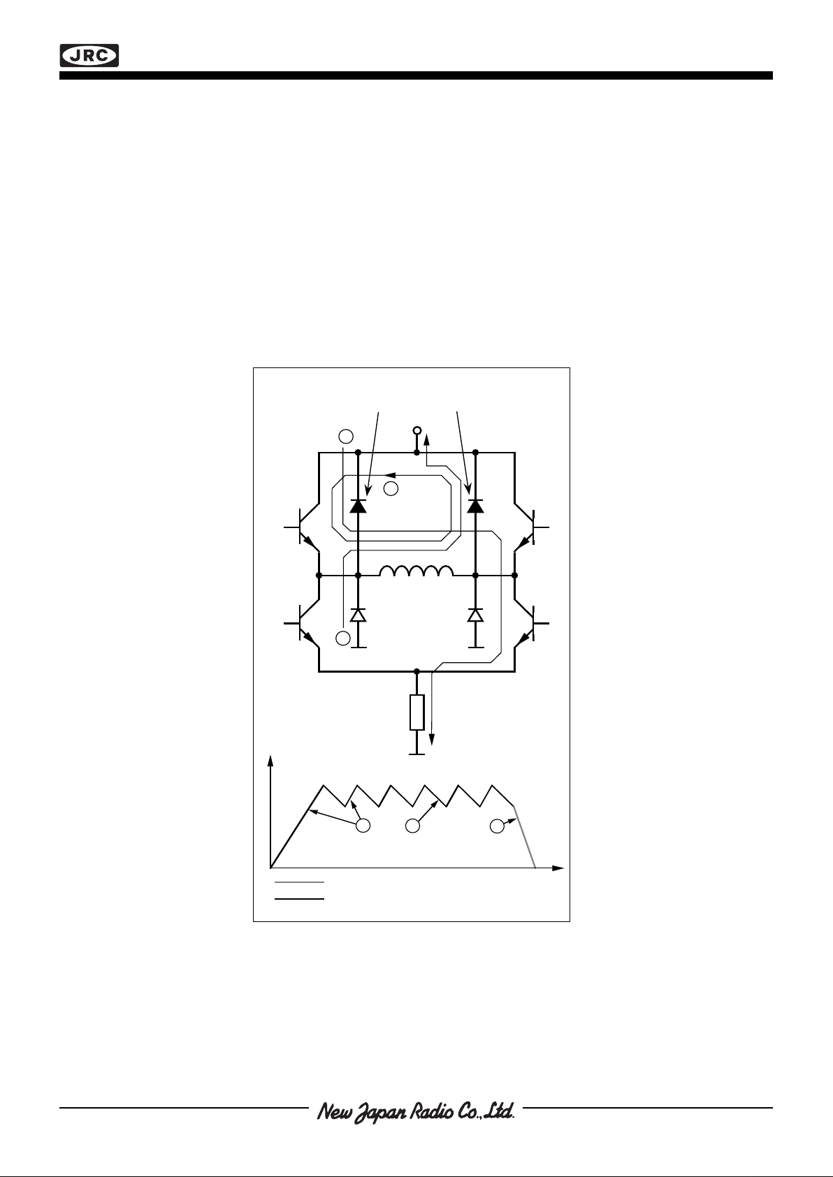
Figure 3. Output stage with current paths
during turn-on, turn-off and phase shift.
■ FUNCTIONAL DESCRIPTION
Each channel of the NJM3774 consists of the following sections: an output H-bridge with four transistors, capable
of driving up to 1000mA continuous current to the motor winding; a logic section that controls the output transistors;
an S-R flip-flop; and a comparator. The clock-oscillator is common to both channels.
Constant current control is achieved by switching the output current to the windings. This is done by sensing the
peak current through the winding via a resistor, RS, effectively connected in series with the motor winding during the
turn-on period. As the current increases, a voltage develops across the resistor, and is fed back to the comparator.
At the predetermined level defined by the voltage at the reference input VR, the comparator resets the flip-flop,
turning off the output transistors. The current decreases until the clock oscillator triggers the flip-flop, turning on the
output transistors, and the cycle is repeated.
The current paths during turn-on, turn-off and phase shift are shown in figure 3. Note that the upper recirculation
diodes are connected to the circuit externally.
Fast Current Decay
Slow Current Decay
Motor Current
Time
1 2
3
3
1
2
R
S
V
MM
External recirculation diodes
Page 4

NJM3774
■ ABSOLUTE MAXIMUM RATINGS
Parameter Pin no. [DIP-package] Symbol Min Max Unit
Voltage
Logic supply 22 V
CC
07 V
Motor supply 9, 14 V
MM
045 V
Logic inputs 4, 7, 16, 19 V
I
-0.3 6 V
Comparator inputs 2, 21 V
C
-0.3 V
CC
V
Reference inputs 3, 20 V
R
-0.3 7.5 V
Current
Motor output current 8, 11, 12, 15 I
M
-1200 +1200 mA
Logic inputs 4, 7, 16, 19 I
I
-10 - mA
Analog inputs 2, 3, 20, 21 I
A
-10 - mA
Temperature
Operating Junction temperature T
j
-40 +150 °C
Storage temperature T
stg
-55 +150 °C
Power Dissipation (Package Data)
Power dissipation at T
GND
= +25°C, DIP and PLCC package P
D
-5 W
Power dissipation at T
GND
= +125°C, DIP package P
D
- 2.2 W
Power dissipation at T
GND
= +125°C, PLCC package P
D
- 2.6 W
■ RECOMMENDED OPERATING CONDITIONS
Parameter Symbol Min Typ Max Unit
Logic supply voltage V
CC
4.75 5 5.25 V
Motor supply voltage V
MM
10 - 40 V
Motor output current I
M
-1000 - +1000 mA
Operating Junction temperature T
J
- 20 - +125 °C
Rise and fall time, logic inputs t
r, tf
--2µs
Oscillator timing resistor R
T
21520kΩ
Figure 5. Definition of terms
Figure 4. Definition of symbols
I I
M OL
I
CC
I I I
I IH IL
I
A
3 300 pF
V
CC
V
V
V
I
IH
IL
V
V
A
R
V
V
CH
C
I
I
C
A
V
E
V
MM
C
820 pF
1 kW
R
S
R
T
T
C
C
R
C
15 kW
I
MM
I
RC
RC
NJM3774
M
A1
M
B1
M
B2
M
A2
GNDC
2
V
R2
Phase
2
V
CC
C
1
V
R1
Phase
1
E
1
E
2
V
CC
SRQ
+
–
Logic
S
R
Q
+
–
Logic
+
–
V
MM2
V
MM1
Dis
1
Dis
2
9
1
22
11
8
42 3
5, 6, 17, 18
10
14
12
15
13
2120
19 16
7
I
R
V
V
M
MA
50 %
V
CH
t
on
t
off
V
E
| V – V |
MA MB
f =
s
t
ontoff
+
D =
t
t
on
off
+
1
t
on
t
t
t
d
Page 5

NJM3774
■ ELECTRICAL CHARACTERISTICS
Electrical characteristics over recommended operating conditions unless otherwise noted, - 20°C ≤ TJ ≤ +125°C.
Parameter
Symbol Conditions Min Typ Max Unit
General
Supply current I
CC
Note 4. - 60 75 mA
Total power dissipation P
D
VMM = 12 V, IM1 = IM2 = 750 mA. - 2.6 2.9 W
Notes 2, 3, 4.
Total power dissipation P
D
VMM = 12 V, IM1 = 1000 mA, IM2 = 0 mA. - 2.6 2.9 W
Notes 2, 3, 4.
Thermal shutdown junction temperature - 160 - °C
Turn-off delay t
d
TA = +25°C, dVC/dt ≥ 50 mV/µs. - 1.4 2.0 µs
I
M
= 100 mA. Note 3.
Logic Inputs
Logic HIGH input voltage V
IH
2.0 - - V
Logic LOW input voltage V
IL
- - 0.8 V
Logic HIGH input current I
IH
VI = 2.4 V - - 20 µA
Logic LOW input current I
IL
VI = 0.4 V -0.4 - - mA
Comparator Inputs
Threshold voltage V
CH
RC = 1 kohm, VR = 2.50 V 430 450 470 mV
| V
CH1
- V
CH2
| mismatch V
CH,diffRC
= 1 kohm - 1 - mV
Input current I
C
-10 - 1 µA
Reference Inputs
Input resistance R
R
TA = +25°C - 5 - kohm
Input current I
R
VR = 2.5 V - 0.5 1.0 mA
Motor Outputs
Lower transistor saturation voltage I
M
= 750 mA - 0.6 0.9 V
Lower transistor leakage current V
MM
= 41 V, VE = VR = 0 V, VC = V
CC
- - 700 µA
Lower diode forward voltage drop I
M
= 750 mA - 1.2 1.5 V
Upper transistor saturation voltage I
M
= 750 mA. - 1.1 1.4 V
Upper transistor leakage current V
MM
= 41 V, VE = VR = 0 V, VC = V
CC
- - 700 µA
Chopper Oscillator
Chopping frequency f
s
CT = 3300 pF, RT = 15 kohm 25.0 26.5 28.0 kHz
Notes
1. All voltages are with respect to ground. Currents are positive into, negative out of specified terminal.
2. All ground pins soldered onto a 20 cm
2
PCB copper area with free air convection, TA = +25°C.
3. Not covered by final test program.
4. Switching duty cycle D = 30%, f
s
= 26.5 kHz.
■ THERMAL CHARACTERISTICS
Parameter Symbol Conditions Min Typ Max Unit
Thermal resistance Rth
J-GND
DIP package. - 11 - °C/W
Rth
J-A
DIP package. Note 2. - 40 - °C/W
Rth
J-GND
PLCC package. - 9 - °C/W
Rth
J-A
PLCC package. Note 2. - 35 - °C/W
Page 6

NJM3774
Figure 6. Typical stepper motor driver application with NJM3774.
D1 D2
Phase
Dis
V
Phase
Dis
V
1
1
2
2
R1
R2
ECECGND
RC
NJM3774
15 kΩ
3300 pF
820 pF
0.68 Ω
1 kΩ 1 kΩ
0.68 Ω
820 pF
STEPPER
MOTOR
M
M
M
M
A1
B1
A2
B2
V
MM
V
CC
VV
MM1 MM2
+5 V
+5 V
12
8
4
7
19
18
20
22 11 5
23
1, 2,
3, 9,
13, 14,
15, 16,
17, 28.
10 24 6
21
11
2
2
R
S
R
S
26
27
25
V
MM
D3 D4
D1 - D4 are UF 4001 or
BYV 27, t ≤ 100 ns.
rr
Pin numbers refer to
PLCC package.
GND (V )
CC
0.1 µF
+
10 µF
■ APPLICATIONS INFORMATION
Current control
The output current to the motor is de-termined by the voltage at the reference input and value of sensing resistor,
RS.
Chopping frequency, winding induc-tance and supply voltage also affect the current, but to much less extent. The
output current can be switched off com-pletely by a HIGH input level at the Dis-able input (Dis1 and Dis2 for
respective channels). When Disable goes HIGH, all four transistors in the output stage are switched off, and the
output current rapidly drops to zero (“fast current decay” – see figure 3).
The peak motor current through the sensing resistor and the motor winding can be expressed as:
I
M,peak
= 0.18 • ( VR / RS )[A]
A 2.5 V reference voltage and a 0.47 ohm sensing resistor will produce an out-put current level of approximately
960 mA.
To improve noise immunity at the VR input, the voltage control range can be increased to 5 V if RS is correspondingly changed (for example to 1ohm for 900 mA max output current).
External components
For the device to function properly, four external free-wheeling diodes must be connected, as in figure 6. The
diodes should be of fast type with a reverse recovery time of less than 100 ns. Com-monly used types are UF4001
or BYV27.
A low pass filter in series with the com-parator input prevents erroneous switch-ing due to switching transients.The
recommended filter component values, 1 kohm and 820 pF, are suitable for a wide range of motors and operational
conditions.
Since the low-pass filtering action in-troduces a small delay of the signal to the comparator, peak voltage across
the sensing resistor, and hence the peak motor current, will reach a slightly higher level than what is defined by the
comparator threshold, V
CH
, set by the reference input VR (V
CH
= 450 mV at VR= 2.5 V).
The time constant of the low-pass fil-ter may therefore be reduced to minimize the delay and optimize low-current
performance. Increasing the time constant may result in unstable switching. The time constant should be adjusted
by changing the CC value.
Page 7

NJM3774
The frequency of the clock oscillator is set by the RT-CT timing components at the RC pin. The recommended
values result in a clock frequency (= switching frequency) of 26.5 kHz. A lower frequency will result in higher
current ripple, but may improve low-current level linearity. A higher clock frequency reduces current ripple, but
increases the switching losses in the IC and possibly increased iron losses in the motor. If the clock frequency
needs to be changed, the CT capacitor value should be adjusted. The recommended RT resistor value is 15 kohm.
The sensing resistor RS, should be selected for maximum motor current. The relationship between peak motor
current, reference voltage and the value of RS is described under Current control above. Be sure not to exceed the
maximum output current which is 1200mA peak when only one channel is activated. Or recommended output
current, which is 1000mA peak, when both channels is activated.
Motor selection
The NJM3774 is designed for two-phase bipolar stepper motors, i.e. motors that have only one winding per phase.
The chopping principle of the NJM3774 is based on a constant frequency and a varying duty cycle. This scheme
imposes certain restrictions on motor selection. Unstable chopping can occur if the chopping duty cycle exceeds
approximately 50%. See figure 5 for definitions. To avoid this, it is necessary to choose a motor with a low winding
resistance and inductance, i.e. windings with a few turns.
It is not possible to use a motor that is rated for the same voltage as the actual supply voltage. Only rated current
needs to be considered. Typical motors to be used together with the NJM3774 have a voltage rating of 1 to 6 V,
while the supply voltage usually ranges from 12 to 40 V.
Low inductance, especially in combination with a high supply voltage, enables high stepping rates. However, to
give the same torque capability at low speed, the reduced number of turns in the winding of the low resistive, low
inductive motor must be compensated by a higher current. A compromise has to be made. Choose a motor with the
lowest possible winding resistance and inductance, that still gives the required torque, and use as high supply
voltage as possible, without exceeding the maximum recommended 40 V. Check that the chopping duty cycle does
not exceed 50% at max. current.
General
Phase inputs
A logic HIGH on a Phase input gives a current flowing from pin MA into MB. A logic LOW gives a current flow in the
opposite direction. A time delay prevents cross conduction in the H-bridge when changing the Phase input.
Heat sinking
Soldering the batwing ground leads onto a copper ground plane of 20 cm2 (approx. 1.8" x 1.8"), copper foil
thickness 35 µm, permits the circuit to operate with 650 mA output current, both channels driving, at ambient
temperatures up to 70°C. Consult figures 7,10 and 11 in order to determine the necessary copper ground plane
area for heat sinking at higher current levels.
Thermal shutdown
The circuit is equipped with a thermal shutdown function that turns the output off at temperatures above 160°C.
Normal operation is resumed when the temperature has decreased.
Figure 8. Stepping modes
V
R1
Dis
1
Phase
1
Phase
2
Dis
2
I
MA1
I
MA2
100%
–100%
–100%
100%
Full step mode Half step mode Modified half step mode
V
R2
140%
100%
140%
100%
140%
–140%
140%
–140%
Thermal resistance [°C/W]
PCB copper foil area [cm ]
2
80
70
60
50
40
30
20
5101520
30 3525
PLCC package
DIP package
28-Pin
PLCC
22-Pin
DIP
Figure 7. Typical thermal resistance vs. PC Board copper
area and suggested layout
Page 8

NJM3774
Programming
Figure 8 shows the different input and output sequences for full-step, half-step and modified halfstep operations.
Full-step mode
Both windings are energized at all the time with the same current, IM1 = IM2. To make the motor take one step, the
current direction (and the magnetic field direction) in one phase is reversed. The next step is then taken when the
other phase current reverses. The current changes go through a sequence of four different states which equal four
full steps until the initial state is reached again.
Half-step mode
In the half-step mode, the current in one winding is brought to zero before a complete current reversal is made. The
motor will then have taken two half steps equalling one full step in rotary movement. The cycle is repeated, but on
the other phase. A total of eight states are sequenced until the initial state is reached again.
Half-step mode can overcome potential resonance problems. Resonances appear as a sudden loss of torque at
one or more distinct stepping rates and must be avoided so as not to loose control of the motor´s shaft position.
One disadvantage with the half-step mode is the reduced torque in the half step positions, in which current flows
through one winding only. The torque in this position is approximately 70 % of the full step position torque.
Modified half-step mode.
The torque variations in half step mode will be elimi-nated if the current is increased about 1.4 times in the halfstep
position. A constant torque will further reduce resonances and mechanical noise, resulting in better performance,
life expectancy and reliability of the mechanical system.
Modifying the current levels must be done by bringing the reference voltage up (or down) from its nominal value
correspondingly. This can be done by using DACs or simple resistor divider networks, as shown in figure 9.
The NJM3774 is designed to handle about 1.4 times higher current in one channel on mode, for example 700
mA per winding in the full-step position, and 1000 mA in the half-step position.
70 % current
level
GND
+5 V
Ref
V
1.2 kΩ
10 kΩ
2.2 kΩ
1.2 kΩ
10 nF
V and
V on
NJM3774
R1
R2
Figure 9. Reduction of reference
voltage at the VR pin of NJM3774
Page 9

NJM3774
Figure 10. Power dissipation vs.
motor current,TA = 25°C
Figure 12. Typical lower transistor
saturation voltage vs. output current
Figure 13. Typical lower diode voltage
drop vs. recirculating current
Figure 14. Typical upper transistor
saturation voltage vs. output current
Figure 11. Maximum allowable
continuous power dissipation vs.
temperature
■ TYPICAL CHARACTERISTICS
The specifications on this databook are only
given for information , without any guarantee
as regards either mistakes or omissions.
The application circuits in this databook are
described only to show representative
usages of the product and not intended for
the guarantee or permission of any right
including the industrial rights.
PD (W)
I
M
(A)
3.0
2.0
1.0
0
0 0.20 0.40 0.60 0.80
O
ne channel on
O
ne channel on
O
ne channel on
Two channels on
Maximum allowable power dissipation [W]
Temperature [°C]
0 25 50 75 125 150
100
PLCC package
DIP package
All ground pins soldered onto a
20 cm PCB copper area with
free air convection.
2
6
5
4
3
2
1
0
Batwing pin temperature
Ambient temperature
-25
V
CE Sat
(V)
I
M
(A)
0 0.20 0.40 0.60 0.80
1.2
0.8
0.4
0
0.2
0.6
1.0
V
d, ld
(V)
I
M
(A)
0 0.20 0.40 0.60 0.80
1.2
0.8
0.4
0
0.2
0.6
1.0
V
CE Sat
(V)
I
M
(A)
0 0.20 0.40 0.60 0.80
1.2
0.8
0.4
0
0.2
0.6
1.0
 Loading...