

Page 1
DUAL STEPPER MOTOR DRIVER
■ GENERAL DESCRIPTION ■ PACKAGE OUTLINE
The NJM3771 is a stepper motor driver, which circuit is
especially developed for use in microstepping applications in
conjunction with the matching dual DAC (Digital-to-Analog
Converter) NJU39610.
The NJM3771 contains a clock oscillator, which is common
for both driver channels; a set of comparators and flip-flops
imple menting the switching control; and two H-bridges with
internal recirculation diodes. Voltage supply requirements are
+5 V for logic and +10 to +45 V for the motor. Maximum
output current is 650 mA per channel.
NJM3771D2
NJM3771
NJM3771E3
■ FEATURES
• Dual chopper driver
• 650 mA output current per channel
• Selectable slow/fast current decay for improved high-
speed microstepping
• Specially matched to Dual DAC NJU39610
• Packages DIP22 / EMP24(Batwing) / PLCC28
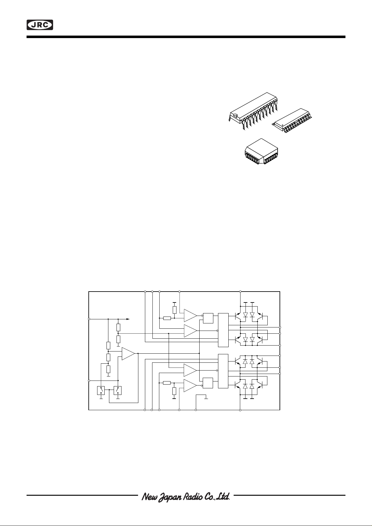
■ BLOCK DIAGRAM
VR1CD
1
1
V
CC
RC
NJM3771
Phase
V
CC
+
–
NJM3771FM2
C
1
–
+
+
–
–
+
+
–
R
S
SRQ
Q
Logic
Logic
E
1
M
A1
M
B1
V
MM1
V
MM2
M
B2
M
A2
Figure 1. Block diagram
Phase
VR2CD
2
2
GNDC
2
E
2
Page 2
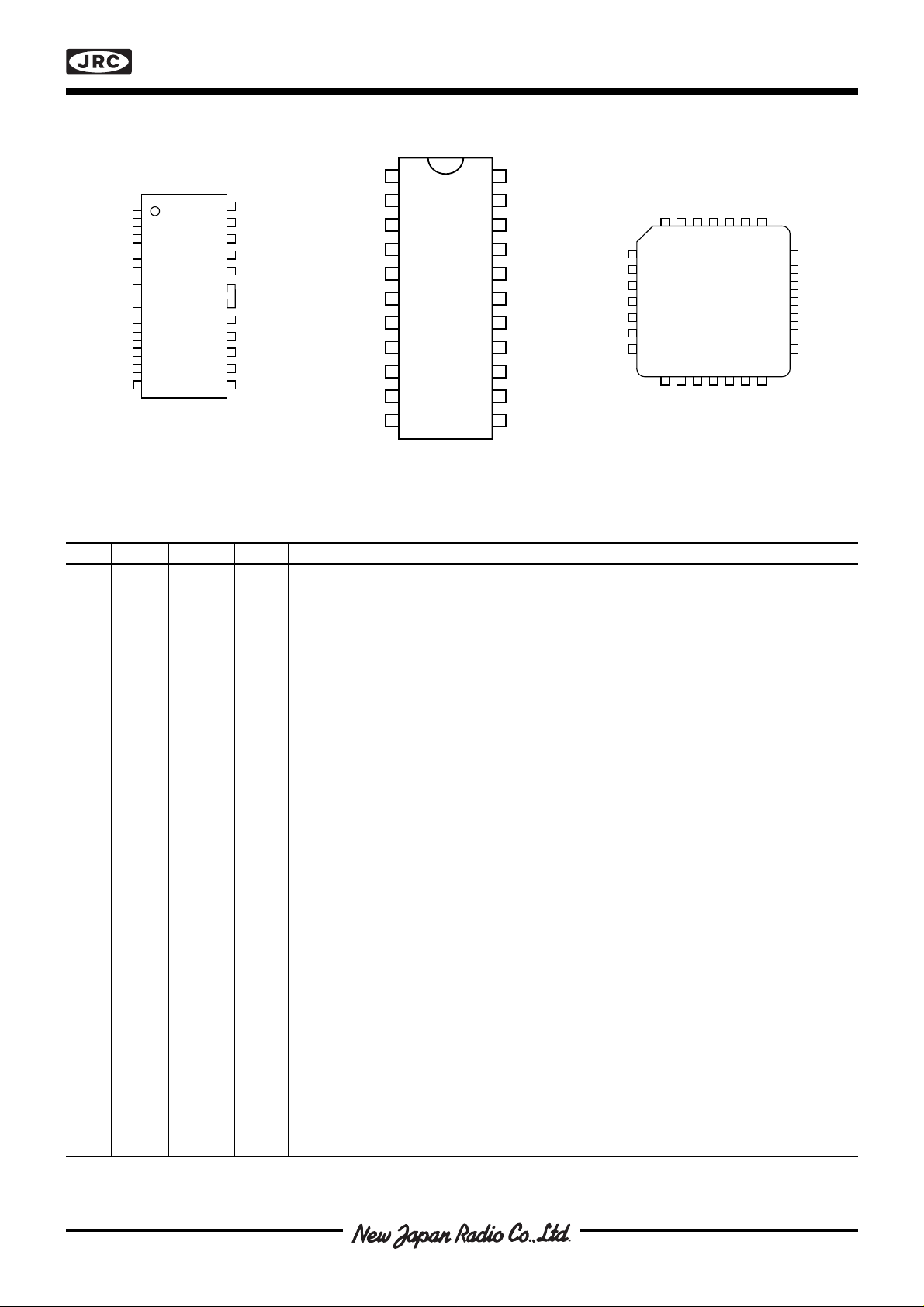
■ PIN CONFIGURATIONS
1
2
3
4
5
6
8
9
10
11
22
21
20
19
18
17
16
15
14
1312
GND
MA
1
MA
2
GND
NC
NJM
3771E3
MB
1
E
1
VMM
1
NC
MB
2
E
2
VMM
2
VR
2
CD
2
C
2
RC
23
24
GND
GND
Phase
2
7
VR
1
CD
1
C
1
V
CC
Phase
1
NJM3771
M
V
MM1
M
GND
GND
Phase
CD
V
V
E
C
CC
B1
A1
R1
1
1
1
1
1
2
3
4
5
6
7
8
9
10
11
NJM
3771D2
22
21
20
19
18
17
16
15
14
13
12
M
B2
E
2
V
MM2
M
A2
GND
GND
Phase
CD
2
V
R2
C
2
RC
2
A2
M
GND
GND
GND
GND
GND
1
GND
432
5
V
MM2
E
6
2
M
7
B2
M
8
B1
NJM 3771FM2
GND
2
9
10
E
1
V
11
MM1
12131415161718
A1
M
GND
Phase
282726
GND
GND
2
CD
1
Phase
25
V
R2
C
24
2
RC
23
V
22
CC
C
21
1
20
V
R1
19
CD
1
Figure 2. Pin configurations
■ PIN DESCRIPTION
Refer to Figure 2
EMP DIP PLCC Symbol Description
218MB1Motor output B, channel 1. Motor current flows from MA1 to MB1 when Phase1 is HIGH.
3210E
4311V
5412MA1Motor output A, channel 1. Motor current flows from MA1 to MB1 when Phase1 is HIGH.
6,7, 5,6, 1-3,9, GND Ground and negative supply. Note: these pins are used thermally for heat-sinking.
18,19 17,18 13-17,28 Make sure that all ground pins are soldered onto a suitably large copper ground
8 7 18 Phase
9819CD
10 9 20 V
11 10 21 C
12 11 22 V
13 12 23 RC Clock oscillator RC pin. Connect a 15 kohm resistor to VCC and a 3300 pF capacitor to
14 13 24 C
15 14 25 V
16 15 26 CD2Current decay control, channel 2. A logic HIGH on this input results in
17 16 27 Phase
20 19 4 M
21 20 5 V
22 21 6 E
23 22 7 M
Common emitter, channel 1. This pin connects to a sensing resistor to ground.
1
Motor supply voltage, channel 1, 10 to 40 V. V
MM1
MM1
and V
should be connected together.
MM2
plane for efficient heat sinking.
Controls the direction of motor current at outputs MA1 and MB1. Motor current flows from M
1
to MB1 when Phase1 is HIGH.
Current decay control, channel 1. A logic HIGH on this input results in
1
a LOW results in
Reference voltage, channel 1. Controls the threshold voltage for the comparator and hence
R1
fast
current decay, see “Functional Description.”
slow
current decay,
the output current. Input resistance is typically 2.5 kohms, ±20%.
Comparator input channel 1. This input senses the instantaneous voltage across the
1
sensing resistor, filtered by an RC network. The threshold voltage for the comparator is
(0.450 / 2.5) • VR1, i.e. 450 mV at VR1 = 2.5 V.
Logic voltage supply, nominally +5 V.
CC
ground to obtain the nominal switching frequency of 26.5 kHz.
Comparator input channel 2. This input senses the instantaneous voltage across the
2
sensing resistor, filtered by an RC network. The threshold voltage for the comparator is
(0.450 / 2.5) • VR1, i.e. 450 mV at VR1 = 2.5 V.
Reference voltage, channel 2. Controls the threshold voltage for the comparator and hence
R2
the output current. Input resistance is typically 2.5 kohms, ±20%.
slow
current decay,
a LOW results in
Controls the direction of motor current at outputs MA2 and MB2. Motor current flows from M
2
fast
current decay, see “Functional Description.”
to MB2 when Phase2 is HIGH.
Motor output A, channel 2. Motor current flows from MA2 to MB2 when Phase2 is HIGH.
A2
Motor supply voltage, channel 2, 10 to 40 V. V
MM2
Common emitter, channel 2. This pin connects to a sensing resistor to ground.
2
Motor output B, channel 2. Motor current flows from MA2 to MB2 when Phase2 is HIGH.
B2
MM1
and V
should be connected together.
MM2
A1
A2
Page 3
NJM3771
■ FUNCTIONAL DESCRIPTION
Each channel of the NJM3771 consists of the following sections: an H-bridge output stage, capable of driving up
to 650 mA continuous motor current (or 500 mA, both channels driven), a logic section that controls the output
transistors, an S-R flip-flop, and two comparators. The oscillator is common to both channels.
Constant current control is achieved by switching the current to the windings. This is done by sensing the (peak)
voltage across a current-sensing resistor, RS, effectively connected in series with the motor winding, and feeding
that voltage back to a comparator. When the motor current reaches a threshold level, determined by the voltage at
the reference input, VR, the comparator resets the flip-flop, which turns off the output transistors. The current
decreases until the clock oscillator triggers the flip-flop, which turns on the output transistors again, and the cycle is
repeated.
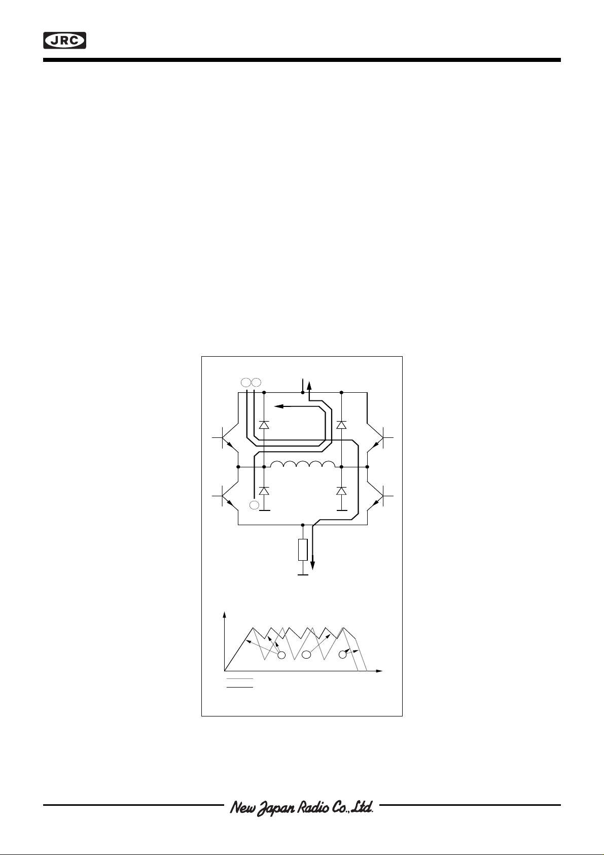
The current-decay rate during the turn-off portion of the switching cycle, can be selected fast or slow by the CD
input.
In slow current-decay mode, only one of the lower transistors in the H-bridge (those closest to the negative
supply) is switched on and off, while one of the upper transistors is held constantly on. During turn-off, the current
recirculates through the upper transistor (which one depends on current direction) and the corresponding freewheeling diode connected to VMM, see figure 3.
In fast current decay mode, both the upper and lower transistors are switched. During the off-time, the freewheeling current is opposed by the supply voltage, causing a rapid discharge of energy in the winding.
Fast current decay may be required in half- and microstepping applications when rapid changes of motor current
are necessary. Slow current decay, however, gives less current ripple, and should always be selected, if possible,
to minimize core losses and switching noise.
Motor Current
1
2
3
R
s
1
32
FAST Current Decay
SLOW Current Decay
Time
Figure 3. Output stage with current paths
during turn -on, turn-off and phase shift
Page 4

NJM3771
50 %
V
CH
t
on
t
off
V
E
| V – V |
MA MB
t
d
t
t
f =
s
tont
off
+
D =
t
t
on
off
+
1
t
on
■ ABSOLUTE MAXIMUM RATINGS
Parameter Pin no. (DIP) Symbol Min Max Unit
Voltage
Logic supply 11 V
Motor supply 3, 20 V
Logic inputs 7, 8, 15, 16 V
Comparator inputs 10, 13 V
Reference inputs 9, 14 V
CC
MM
I
C
R
Current
Motor output current 1, 4, 19, 22 I
Logic inputs 7, 8, 15, 16 I
Analog inputs 10, 13 I
Oscillator charging current 12 I
M
I
A
RC
Temperature
Operating junction temperature T
Storage temperature** T
J
S
** Circuit only. The packaging can handle max 60°C
■ RECOMMENDED OPERATING CONDITIONS
Parameter Symbol Min Typ Max Unit
Logic supply voltage V
Motor supply voltage V
Motor output current *** I
Junction temperature **** T
Rise time logic inputs t
Fall time logic inputs t
Oscillator timing resistor R
CC
MM
M
J
r
f
T
4.75 5 5.25 V
10 - 40 V
-650 - 650 mA
-20 - +125 °C
--2µs
--2µs
2 15 20 kohm
07V
045V
-0.3 6 V
-0.3 V
CC
V
-0.3 7.5 V
-700 +700 mA
-10 - mA
-10 - mA
-5mA
-40 +150 °C
-55 +150 °C
*** In microstepping mode, “sine/cosine” drive where I
= 650 • cos(q) and I2 = 650 • sin(q) mA, otherwise 500 mA/channel both
1
channels fully on.
****See operating temperature chapter.
C
VR1CD
Phase
1
NJM 3771
V
I
CC
CC
11
15 kΩ
R
T
I
RC
RC
12
3 300 pF
V
CC
C
T
I I I
I IH IL
I
V
I
V
IH
V
V
IL
V
A
A
R
7
V
CC
+
–
16
Phase
2
15 14
1
1
10
98
–
R
+
S
+
–
–
+
SRQ
+
–
5, 6, 17, 18
13
VR2CD
2
GNDC
2
I
C
I
A
820 pF
1 kΩ
C
C
V
CH
V
C
Figure 4. Definitions of symbols Figure 5. Definition of terms
E
1
2
Q
Logic
Logic
21
E
2
R
C
R
S
M
4
A1
M
1
B1
V
3
MM1
I
V
20
M
22
M
19
V
E
MM
MM2
B2
I I
M OL
A2
V
V
MM
M
V
MA
Page 5

NJM3771
■ ELECTRICAL CHARACTERISTICS
Electrical characteristics over recommended operating conditions, unless otherwise noted. -20°C < TJ < +125°C
Parameter Symbol Conditions Min Typ Max Unit
General
Supply current I
Total power dissipation P
CC
VMM = 40 V, IM1= 450 mA, IM2= 0 mA. 1.4 1.6 W
D
Notes 2, 3.
V
= 40 V, IM1 = IM2 = 318 mA. 1.6 1.8 W
MM
Notes 2, 3.
Turn-off delay t
Ta = +25°C, dVC/dt ≥ 50 mV/µs. - 1.0 1.5 µs
d
Note 3.
Logic Inputs
Logic HIGH input voltage V
Logic LOW input voltage V
Logic HIGH input current I
Logic LOW input current I
IH
IL
VI = 2.4 V - - 20 µA
IH
VI = 0.4 V -0.4 - - mA
IL
Reference Inputs
Input resistance R
Input current I
Turn-off voltage V
Ta = +25°C - 5 - kohm
R
Ta = +25°C, VR = 2.5 V. 0.5 1.0 mA
R
TO
Comparator Inputs
Threshold voltage V
| V
- V
CH1
| mismatch V
CH2
Input current I
CH,diff
RC = 1 kohms, VR = 2.5 V 430 450 470 mV
CH
RC = 1 kohms - 1 - mV
C
Motor Outputs
Lower transistor saturation voltage I
= 500 mA - 1.00 1.20 V
M
Lower transistor leakage current VMM = 41 V, VE = VR = 0 V, VC = V
Lower diode forward voltage drop I
Upper transistor saturation voltage I
Upper transistor leakage current V
Upper diode forward voltage drop I
= 500 mA - 1.10 1.25 V
M
= 500 mA - 1.20 1.35 V
M
= 41 V, VE = VR = 0 V, VC = V
MM
= 500 mA - 1.00 1.25 V
M
Chopper Oscillator
Chopping frequency f
CT = 3300 pF, RT = 15 kohms 25.0 26.5 28.0 kHz
s
CC
CC
-3850mA
2.0 - - V
- - 0.6 V
20 29 38 mV
-10 - 1 µA
- - 300 µA
- - 300 µA
■ THERMAL CHARACTERISTICS
Parameter Symbol Conditions Min Typ Max Unit
Thermal resistance Rth
Rth
Rth
Rth
Rth
Rth
Notes
1. All voltages are with respect to ground. Currents are positive into, negative out of specified terminal.
2. All ground pins soldered onto a 20 cm
3. Not covered by final test program.
4. Switching duty cycle D = 30%, f
= 26.5 kHz
S
DIP package. - 11 - °C/W
J-GND
DIP package. Note 2. - 40 - °C/W
J-A
PLCC package. - 9 - °C/W
J-GND
PLCC package. Note 2. - 35 - °C/W
J-A
EMP package. - 13 - °C/W
J-GND
EMP package. Note 2. - 42 - °C/W
J-A
2
PCB copper area with free air convection.
Page 6

NJM3771
■ APPLICATIONS INFORMATION
Current control
The output current to the motor winding is mainly determined by the voltage at the reference input and the value of
the sensing resistor, RS.
Chopping frequency, winding inductance, and supply voltage will affect the current level, but to much less extent.
Fast current decay setting will produce somewhat lower (average) current than slow current decay. The peak
current through the sensing resistor (and motor winding) can be expressed as:
I
= 0.18 • (VR / RS)[A]
M,peak
i.e., with a recommended value of 1 ohm for the sensing resistor, RS, a 2.5 V reference voltage will produce an
output current of approximately 450 mA. To improve noise immunity on the VR input, the control range may be
increased to
5 volts if RS is correspondingly changed to 2 ohms.
To
P
+2.5V
+
10 µF
V
MM
V (+5 V)
CC
0.1 µF 0.1 µF
11 3 20
Phase
CD
V
R1
Phase
CD
V
R2
RC
V
1
1
2
2
5, 6,
17, 18
+5 V
7
8
9
16
15
14
12
15 kΩ
3 300 pF
GND
(V )
CC MM
VV
CC
MM1 MM2
NJM3771
11
2
10
1 kΩ 1 kΩ
820 pF 820 pF
1.0 Ω 1.0 Ω
4
M
A1
M
1
B1
19
M
A2
22
M
B2
ECECGND
2
13
2
21
STEPPER
MOTOR
Pin numbers refer
to DIP package.
R
S
R
S
GND (V
)
Figure 6. Typical stepper motor application with NJM3771
V (+5 V)
CC
+
0.1 µF 0.1 µF
14
D0
7
D7
NJU 39610
15
A0
16
A1
6
WR
17
CS
22
RESET
1
VV
Ref
GND
(V )
CC MM
5
V
DD
SS
18
Sign
Sign
3
1
4
CD
1
2
DA
1
20
2
19
CD
2
21
DA
2
+5 V
7
8
9
16
15
14
15 kΩ
3 300 pF
Phase
CD
V
Phase
CD
V
RC
12
11 3 20
V
CC
1
1
R1
R2
2
5, 6,
17, 18
NJM 3771
2
VV
MM1 MM2
11
10
1 kΩ 1 kΩ
820 pF 820 pF
1.0 Ω 1.0 Ω
2
2
13
R
S
M
A1
M
B1
M
A2
M
B2
ECECGND
2
21
R
10 µF
4
1
19
22
STEPPER
Pin numbers refer
to DIP package.
S
GND (V
MOTOR
V
MM
)
Figure 7. Microstepping system with NJU39610 and NJM3771
Page 7

NJM3771
External components
The voltage across the sensing resistor is fed back to the comparator via a low-pass filter section, to prevent
erroneous switching due to switching transients. The recommended filter component values, 1 kohm and 820 pF,
are suitable for a wide range of motors and operational conditions.
Since the low-pass filtering action introduces a small delay of the signal to the comparator, peak voltage across
the sensing resistor, and hence the peak motor current, will reach a slightly higher level than the threshold, VC, set
by the reference voltage
(VC = 450 mV @VR = 2.5 V).
The time constant of the low-pass filter may therefore be reduced to minimize the delay and optimize low-current
performance, especially if a low (12 V) supply voltage is used. Increasing the time constant may result in unstable
switching.
The frequency of the clock oscillator is set by the R-C combination at pin RC. The recommended values give a
nominal frequency of 26.5 kHz. A lower frequency will result in higher current ripple and may cause audible noise
from the motor, while increasing the frequency results in higher switching losses and possibly increased iron losses
in the motor.
The sensing resistor, RS, should be selected for maximum motor current. The relationship between peak motor
current, reference voltage and the value of RS is described under “Current control” above. Be sure not to exceed
the maximum output current which is 650 mA per channel (or 500 mA per channel, both channels fully on, see
“Recommended Operating Conditions”).
Motor selection
The NJM3771 is designed for bipolar motors, i.e., motors that have only one winding per phase. A unipolar motor,
having windings with a center tap, can also be used, see figure 8.
The chopping principle in the NJM3771 is based on a constant frequency and a varying duty cycle. This
scheme imposes certain restrictions on motor selection. Unstable chopping can occur if the chopping duty cycle
exceeds approximately 50%. To avoid this, it is necessary to choose a motor with a low winding resistance. Low
winding resistance means less inductance and will therefore enable higher stepping rates, however it also means
less torque capability. A compromise has to be made.
Choose a motor with the lowest possible winding resistance that still gives the required torque and use as high
supply voltage as possible without exceeding the maximum recommended 40 V. Check that the chopping duty
cycle does not exceed 50% at maximum current.
Since the NJM3771 produces a regulated, constant output current it is not necessary to use a motor that is rated
at the same voltage as the actual supply voltage. Only rated current needs to be considered. Typical motors to be
used together with the NJM3771 have voltage ratings of 5 to 12 V, while the supply voltage usually ranges from 24
to 40 V.
Best for high speed
NJM3771
Figure 8. Connection of unipolar motors
Best for high torque
NJM3771
Page 8

NJM3771
General
Phase inputs
A logic HIGH on a Phase input gives positive current flowing out from MA into MB. A logic LOW gives a current in
the opposite direction.
Slow/fast current decay
A logic HIGH on the CD input gives slow current decay, a logic LOW gives fast current decay.
Heat sinking
Soldering the four center pins onto a free PCB copper area of 20 cm2 (approx. 1.8" x 1.8", copper foil thickness =
35 µm) permits the circuit to operate with a maximum of 320 mA output current, both channels driving, at ambient
temperatures up to +70°C. Consult figures 9 and 14 in order to determine the necessary copper area for heat
sinking if higher currents are required.
Thermal shutdown
The circuit is equipped with a thermal shutdown function that reduces the output current at chip temperatures
above +160°C.
Thermal resistance [°C/W]
80
70
60
50
24-pin EMP
40
30
20
5101520
PCB copper foil area [cm ]
PLCC package
DIP package
30 3525
2
Figure 9. Thermal Resistance vs. PC Board copper area and suggested layout
22-pin
DIP
28-pin
PLCC
Page 9

■ TYPICAL CHARACTERISTICS
Vd (V)
°C
1.0
Tj = 25
V
CE Sat
1.2
(V)
Vd (V)
1.0
NJM3771
°C
Tj = 25
.8
.6
.4
.2
0
0 .10 .20 .30 .40 .50 .60
Tj = 125
IM (A)
°C
Figure 10. Typical upper diode
voltage drop vs. recirculating current
V
(V)
CE Sat
1.0
.8
.6
.4
.2
0 .10 .20 .30 .40 .50 .60
Tj = 25
°C
Tj = 125
IM (A)
°C
1.0
.8
.6
.4
.2
°C
Tj = 25
°C
Tj = 125
0 .10 .20 .30 .40 .50 .60
IM (A)
Figure 11. Typical source saturation
voltage vs. output current
.8
Tj = 125
.6
.4
.2
0
0 .10 .20 .30 .40 .50 .60
Figure 12. Typical lower diode
voltage drop vs. recirculating current
PD (W)
3.0
2.0
VMM = 36V
VMM = 14V
1.0
0
0 .10 .20 .30 .40 .50 .60
Max allow power is
IM (A)
°C
IM (A)
Figure 13 Typical sink saturation
voltage vs. output current
Figure 14. Power dissipation vs. motor current,
both channels driven, Ta = 25°C
The specifications on this databook are only
given for information , without any guarantee
as regards either mistakes or omissions.
The application circuits in this databook are
described only to show representative
usages of the product and not intended for
the guarantee or permission of any right
including the industrial rights.
 Loading...