

Page 1
STEPPER MOTOR DRIVER
■ GENERAL DESCRIPTION ■ PACKAGE OUTLINE
NJM3717 is a stepper motor diver, which consists of a LS-TTL
compatible logic input stage, a current sensor, a monostable
multivibrator and a high power H-bridge output stage with built-in
protection diodes.
The output current is up to 1200mA. Two NJM3717 and a small
number of external components form a complete control and drive
unit for stepper motor systems.
NJM3717D2
NJM3717
NJM3717E2
■ FEATURES
• Half-step and full-step modes
• Switched mode bipolar constant current drive
• Wide range of current control 5 - 1200 mA
• Wide voltage range 10 - 50 V
• Thermal overload protection
• Packages DIP16 / PLCC28 / EMP20
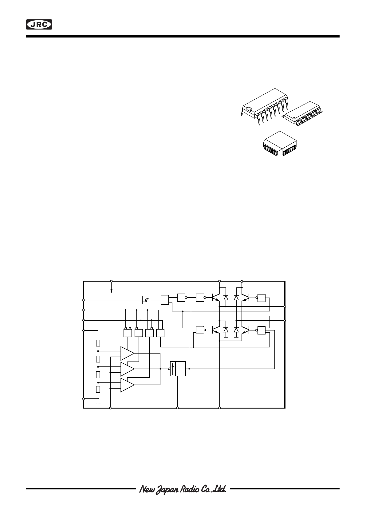
■ BLOCK DIAGRAM
V
CC
Schmitt
Phase
I
1
I
0
V
R
Trigger
& &&&
Time
Delay
1 1
≥ 1
NJM3717FM2
V
MM
V
MM
1
M
A
M
B
≥ 1
GND
Figure 1. Block diagram
+
–
+
–
+
–
Current Sensor
Monostable
t = 0.69 • R • C
off
T
Output Stage
T T
NJM3717
E
Page 2
N/C
A
N/C
E
GND
B
T
N/C
V
C
N/C
I
Phase
I
V
GND
GND
GND
GND
N/C
N/C
MM
GND
GND
GND
GND
GND
CC
5
6
7
8
9
10
11
25
24
23
22
21
20
19
432
1
282726
12131415161718
MM
R
0
1
V
V
M
M
NJM3717FM2
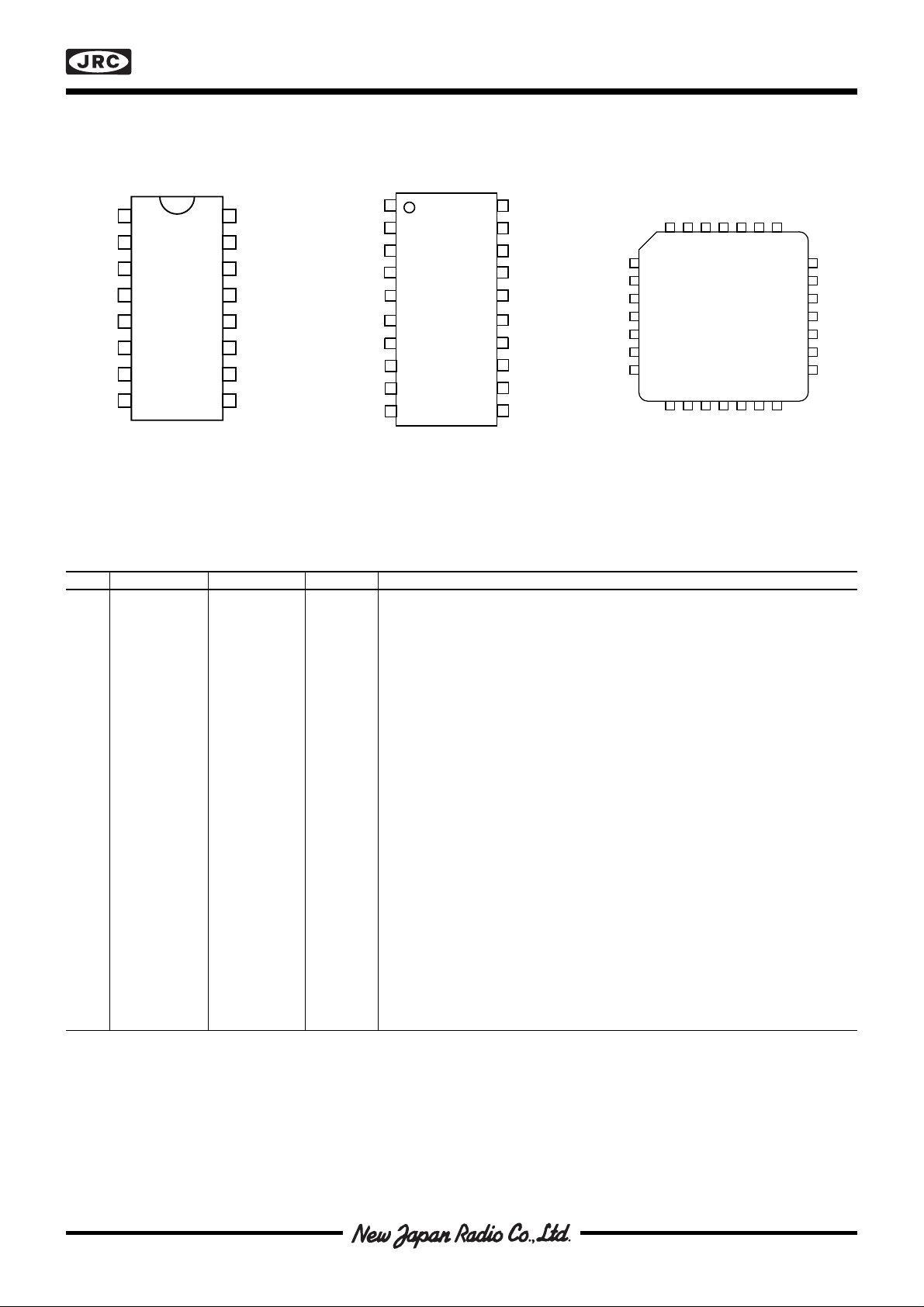
■ PIN CONFIGURATIONS
M
V
MM
GND
GND
V
CC
Phase
B
T
I
1
1
2
3
NJM
4
3717D2
5
6
7
8
E
16
M
15
V
14
GND
13
GND
12
V
11
C
10
I
9
Figure 2. Pin configurations
0
A
MM
R
M
V
MM
GND
GND
GND
GND
V
CC
Phase
NJM3717
1
B
T
2
3
4
5
NJM
3717E2
6
7
8
I
1
9
10
20
E
19
M
A
18
V
MM
17
GND
16
GND
15
GND
14
GND
13
V
R
12
C
11
I
0
■ PIN DESCRIPTION
DIP EMP PLCC Symbol Description
11 10M
2 2 11 T Clock oscillator. Timing pin connect a 56 kΩ resistor and a 820 pF in
3,14 3,18 12,4 V
4,5, 4,5,6,7,14 1,2,3,9,13, PCB.
12,13 15,16,17 14,15,16,17 GND Ground and negative supply. Note these pins are used for heatsinking.
28 Make sure that all ground pins are soldered onto a suitable large copper
68 18V
79 19I
8 10 20 Phase Controls the direction of the motor current of M
911 21 I
10 12 23 C Comparator input. This input senses the instantaneous voltage across the
11 13 24 V
15 19 6 M
16 20 8 E Common emitter. Connect the sense resistor between this pin and ground.
Motor output B, Motor current flows from MA to MB when Phase is high.
B
parallel between T and Ground.
Motor supply voltage, 10 to 45 V. V
MM
pins should be wired together on
MM
ground plane for efficient heat sinking.
Logic voltage supply normally +5 V.
CC
Logic input, it controls, together with the I0 input, the current level in the
1
output stage. The controllable levels are fixed to 100, 60, 20, 0%.
and MB outputs. Motor
current flows from MA to MB when the phase input is high.
Logic input, it controls, together with the I1 input, the current level in the
0
output stage. The controlable levels are fixed to 100, 60, 20, 0%.
A
sensing resistor, filtered through a RC Network.
Reference voltage. Controls the threshold voltage of the comparator and
R
hence the output current. Input resistance: typically 6.8kΩ ± 20%.
Motor output A, Motor current flows from MA to MB when Phase is high.
A
Page 3
| V – V |
MA MB
NJM3717
t
off
t
t
d
t
t
D =
on
+
t
t
on
off
50 %
V
CH
V
E
f =
s
t
ontoff
t
on
1
+
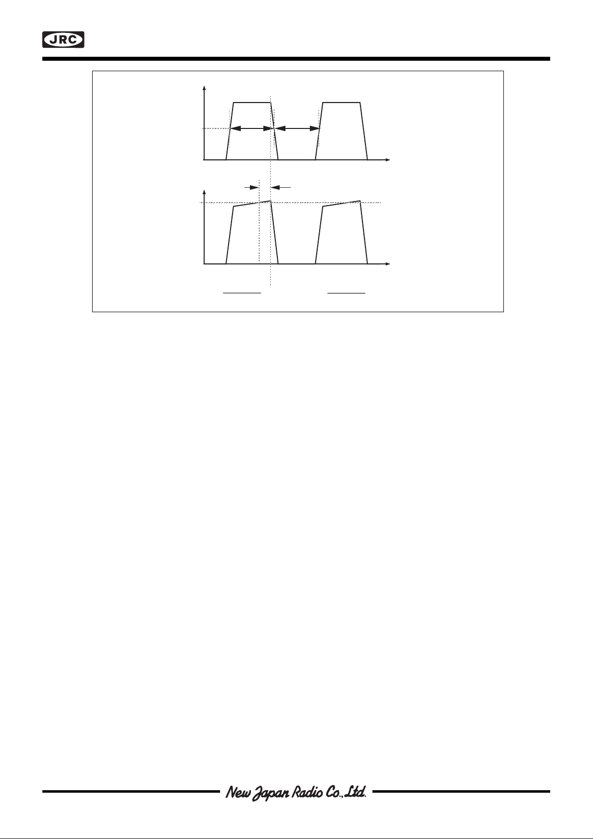
Figure 3. Definition of terms
■ FUNCTIONAL DESCRIPTION
The NJM3717 is intended to drive a bipolar constant current through one motor winding of a 2-phase stepper
motor.
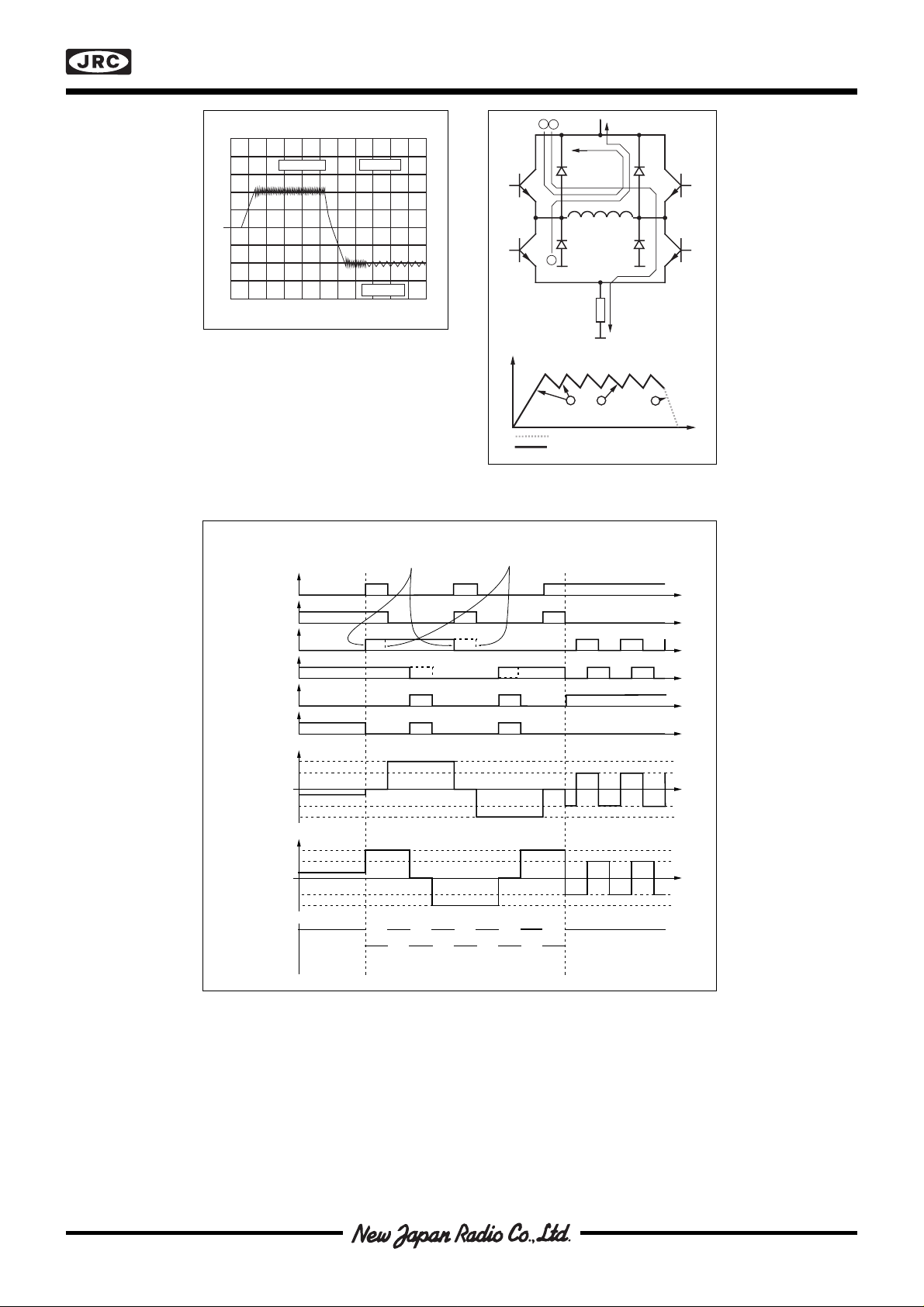
Current control is achieved through switched-mode regulation, see figure 4 and 5.
Three different current levels and zero current can be selected by the input logic.
The circuit contains the following functional blocks:
• Input logic
• Current sense
• Single-pulse generator
• Output stage
Input logic
Phase input. The phase input determines the direction of the current in the motor winding. High input forces the
current from terminal MA to MB and low input from terminal MB to MA. A Schmitt trigger pro vides noise immunity and
a delay circuit eliminates the risk of cross conduction in the output stage during a phase shift.
Half- and full-step operation is possible.
Current level selection. The status of I0 and I1 inputs determines the current level in the motor winding. Three fixed
current levels can be selected according to the table below.
Motor current I
I
0
1
High level 100% L L
Medium level 60% H L
Low level 20% L H
Zero current 0% H H
The specific values of the different current levels are determined by the reference voltage VR together with the value
of the sensing resistor RS.
The peak motor current can be calculated as follows:
im = (VR • 0.083) / RS [A], at 100% level
im = (VR • 0.050) / RS [A], at 60% level
im = (VR • 0.016) / RS [A], at 20% level
The motor current can also be continuously varied by modulating the voltage reference input.
Page 4
NJM3717
Current sensor
The current sensor contains a reference voltage divider and three comparators for measuring each of the selectable current levels. The motor current is sensed as a voltage drop across the current sensing resistor , RS, and
compared with one of the voltage references from the divider. When the two voltages are equal, the comparator
triggers the single-pulse generator. Only one comparator at a time is activated by the input logic.
Single-pulse generator
The pulse generator is a monostable multivibrator triggered on the positive edge of the comparator output. The
multivibrator output is high during the pulse time, t
t
= 0.69 • RT • C
off
T
The single pulse switches off the power feed to the motor winding, causing the winding to decrease during t
new trigger signal should occur during t
, it is ignored.
off
Output stage
The output stage contains four transistors and four diodes, connected in an H-bridge. The two sinking transistors
are used to switch the power supplied to the motor winding, thus driving a constant current through the winding.
See figures 4 and 5.
Overload protection
The circuit is equipped with a thermal shut-down function, which will limit the junction temperature. The output
current will be reduced if the maximum permissible junction temperature is exceeded. It should be noted, however,
that it is not short circuit protected.
Operation
When a voltage VMM is applied across the motor winding, the current rise follows the equation:
im = (VMM / R) • (1 - e
-(R • t ) / L
)
R = Winding resistance
L = Winding inductance
t = time
(see figure 5, arrow 1)
The motor current appears across the external sensing resistor, RS, as an analog voltage. This voltage is fed
through a low-pass filter, RCCC, to the voltage comparator input (pin 10). At the moment the sensed voltage rises
above the comparator threshold voltage, the monostable is triggered and its output turns off the conducting sink
transistor.
The polarity across the motor winding reverses and the current is forced to circulate through the appropriate
upper protection diode back through the source transistor (see figure 5, arrow 2).
After the monostable has timed out, the current has decayed and the analog voltage across the sensing resistor is
below the comparator threshold level.
The sinking transistor then closes and the motor current starts to increase again, The cycle is repeated until the
current is turned off via the logic inputs.
By reversing the logic level of the phase input (pin 8), both active transistors are turned off and the opposite pair
turned on after a slight delay. When this happens, the current must first decay to zero before it can reverse. This
current decay is steeper because the motor current is now forced to circulate back through the power supply and
the appropriate sinking transistor protection diode. This causes higher reverse voltage build-up across the winding
which results in a faster current decay (see figure 5, arrow 3).
For best speed performance of the stepper motor at half-step mode operation, the phase logic level should be
changed at the same time the current-inhibiting signal is applied (see figure 6).
, which is determined by the timing components RT and CT.
off
off
.If a
Page 5
200 mA/div 1 ms/div
Fast Current Decay
Slow Current Decay
Motor Current
Time
1 2
3
0
100µs/div
Figure 4. Motor current (IM ),
Vertical : 200 mA/div, Horizontal: 1
ms/div, expanded part 100 µs/div
NJM3717
2
1
3
R
S
Figure 5. Output stage with current
paths for fast and slow current decay
I
I
Ph
Ph
I
I
I
100%
60%
–20%
–60%
–100%
I
100%
60%
20%
–60%
–100%
Full step position
Half step position
Phase shift here
gives fast
current decay
0A
1A
A
B
0B
1B
MA
MB
at 20 %
Half step mode at 100 % Full step mode at 60 %Stand by mode
Phase shift here
gives slow
current decay
Figure 6. Principal operating sequence
Page 6
NJM3717
■ ABSOLUTE MAXIMUM RATINGS
Parameter Pin [DIP] Symbol Min Max Unit
Voltage
Logic supply 6 V
Motor supply 3, 14 V
Logic inputs 7, 8, 9 V
Comparator input 10 V
Reference input 11 V
CC
MM
I
C
R
Current
Motor output current 1, 15 I
Logic inputs 7, 8, 9 I
Analog inputs 10, 11 I
M
I
A
Temperature
Operating junction temperature T
Storage temperature T
j
stg
■ RECOMMENDED OPERATING CONDITIONS
Parameter Symbol Min Typ Max Unit
Logic supply voltage V
Motor supply voltage V
Motor output current I
Operating junction temperature T
Rise time logic inputs t
Fall time logic inputs t
CC
MM
M
j
r
f
4.75 5 5.25 V
10 - 45 V
-1000 - +1000 mA
-20 - +125 °C
-- 2µs
-- 2µs
07V
050V
-0.3 6 V
-0.3 V
CC
V
-0.3 15 V
-1200 +1200 mA
-10 - mA
-10 - mA
-40 +150 °C
-55 +150 °C
I
CC
V
CC
6
I I I
I IH IL
V
V
I
CC
V
IH
V
IL
Phase
8
7
I
1
1
9
I
I
0
V
I
V
A
V
R
V
11
GND
R
4, 5,
12, 13
10
C
C
I
C
I
A
V
C
V
CH
820 pF
C
C
A
& &&&
+
–
+
–
+
–
Current Sensor
1 kΩ
Schmitt
Trigger
R
Time
Delay
1
1
≥1
Monostable
t = 0.69 • R • C
off
2
T
T
C
56 kΩ
820 pF
C
T
T
T T
V
V
MM
14
MM
3
1
15
1
≥1
Output Stage
16
E
E
1Ω
RR
NJM3717
V
S
Pin no. referens
to DIL package
E
I
MM
I I
M
A
M OL
M
B
V
V
MM
M
V
MA
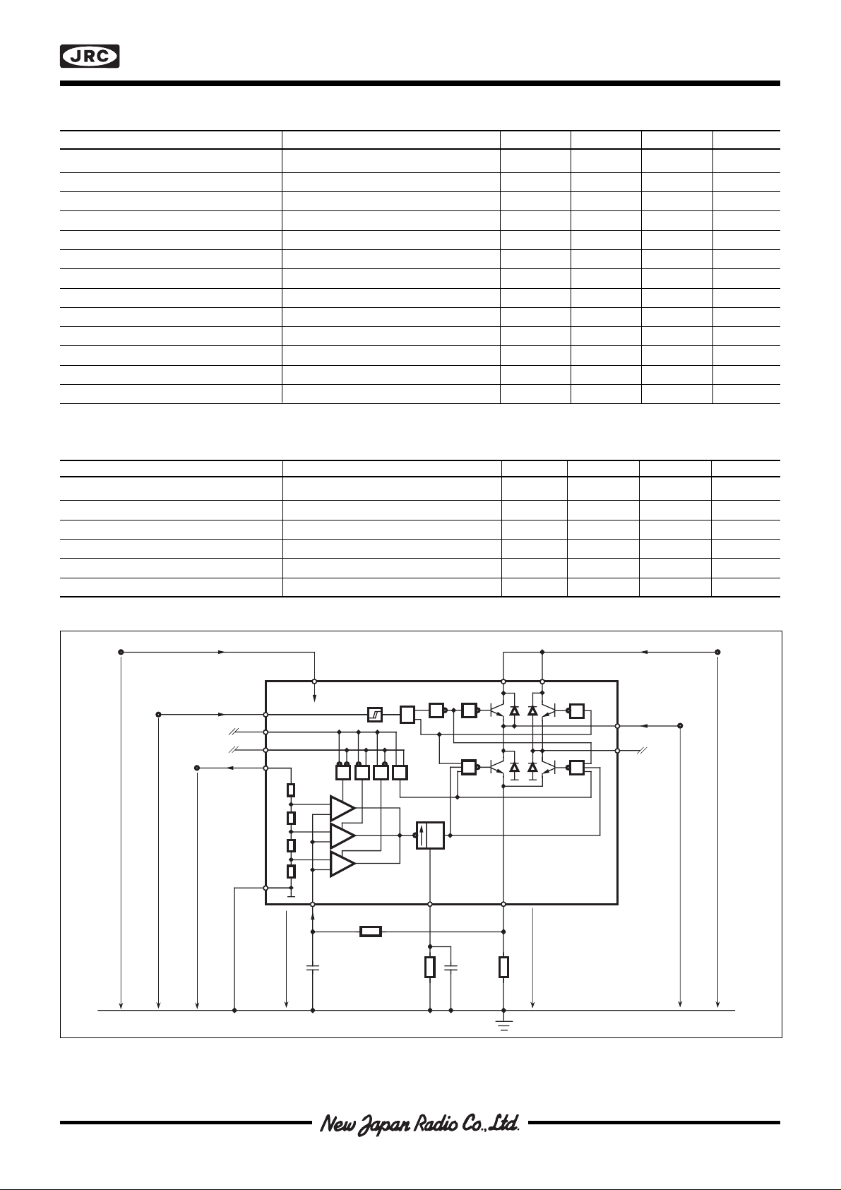
Figure7. Definition of symbols
Page 7
NJM3717
■ ELECTRICAL CHARACTERISTICS
Electrical characteristics over recommended operating conditions, unless otherwise noted -20°C≤ TJ≤ +125°C.
C
= 820 pF, RT = 56 kohm.
T
Parameter Symbol Conditions Min Typ Max Unit
General
Supply current I
CC
Total power dissipation PDfs = 28 kHz, IM = 500mA, VMM = 36 V - 1.4 1.7 W
Note 2, 4.
f
= 28 kHz, IM = 800mA, VMM = 36 V - 2.8 3.3 W
s
Note 3, 4.
Turn-off delay t
T
d
= +25°C, dVC/dt ≥ 50 mV/µs. - 0.9 1.5 µs
a
Thermal shutdown junction temperature - 170 - °C
Logic Inputs
Logic HIGH input voltage V
Logic LOW input voltage V
Logic HIGH input current I
Logic LOW input current I
IH
IL
VI = 2.4 V - - 20 µA
IH
VI = 0.4 V -0.4 - - mA
IL
Reference Input
Input resistance RRTa = +25°C - 6.8 - kohm
Comparator Inputs
Threshold voltage V
Threshold voltage V
Threshold voltage V
Input current I
CMVR
= 5.0 V, I0 = I1 = LOW 400 415 430 mV
CHVR
= 5.0 V, I0 = HIGH, I1 = LOW 240 250 265 mV
= 5.0 V, I0 = LOW, I1 = HIGH 70 80 90 mV
CLVR
C
Motor Outputs
Lower transistor saturation voltage IM = 500 mA - 0.9 1.2 V
IM = 800 mA - 1.1 1.4 V
Lower diode forward voltage drop I
= 500 mA - 1.2 1.5 V
M
IM = 800 mA - 1.3 1.7 V
Upper transistor saturation voltage IM = 500 mA - 1.0 1.25 V
IM = 800 mA - 1.2 1.5 V
Upper diode forward voltage drop IM = 500 mA - 1.0 1.25 V
IM = 800 mA - 1.2 1.45 V
Output leakage current I0 = I1 = HIGH, Ta = +25°C - - 100 µA
Monostable
Cut off time t
V
off
= 10 V, t
MM
≥ 5 µs 273135µs
on
■ THERMAL CHARACTERISTICS
--25mA
2.0 - - V
- - 0.8 V
-20 - - µA
Parameter Symbol Conditions Min Typ Max Unit
Thermal resistance Rthj-
Rth
Rthj-
Rth
Rthj-
Rth
DIP package. - 11 - °C/W
GND
DIP package. Note 2. - 40 - °C/W
J-A
PLCC package. - 9 - °C/W
GND
PLCC package. Note 2. - 35 - °C/W
J-A
EMP package - 11 - °C/W
GND
EMP package - 40 - °C/W
J-A
Notes
1. All voltages are with respect to ground. Currents are positive into, negative out of specified terminal.
2. All ground pins soldered onto a 20 cm2 PCB copper area with free air convection. TA +25°C.
3. DIP package with external heatsink (Staver V7) and minimal copper area. Typical Rth
4. Not covered by final test program.
= 27.5°C/W . TA = +25°C.
J-A
Page 8
NJM3717
■ Applications Information
Motor selection
Some stepper motors are not designed for continuous operation at maximum current. As the circuit drives a constant current through the motor, its temperature can increase, both at low- and high-speed operation.
Some stepper motors have such high core losses that they are not suited for switched-mode operation.
Interference
As the circuit operates with switched-mode current regulation, interference-generation problems can arise in some
applications. A good measure is then to decouple the circuit with a 0.1 µF ceramic capacitor, located near the
package across the power line VMM and ground.
Also make sure that the VR input is sufficiently decoupled. An electrolytic capacitor should be used in the +5 V rail,
close to the circuit.
The ground leads between RS, CC and circuit GND should be kept as short as possible. This applies also to the
leads connecting RS and RC to pin 16 and pin 10 respectively.
In order to minimize electromagnetic interference, it is recommended to route MA and MB leads in parallel on the
printed circuit board directly to the terminal connector. The motor wires should be twisted in pairs, each phase
separately, when installing the motor system.
Unused inputs
Unused inputs should be connected to proper voltage levels in order to obtain the highest possible noise immunity.
Ramping
A stepper motor is a synchronous motor and does not change its speed due to load variations. This means that the
torque of the motor must be large enough to match the combined inertia of the motor and load for all operation
modes. At speed changes, the requires torque increases by the square, and the required power by the cube of the
speed change. Ramping, i.e., controlled acceleration or deceleration must then be considered to avoid motor pullout.
V
, V
CC
MM
The supply voltages, VCC and V
, can be turned on or off in any order. Normal dV/dt values are assumed.
MM
Before a driver circuit board is removed from its system, all supply voltages must be turned off to avoid destructive transients from being generated by the motor.
Phase
Phase
I
1A
I
0A
I
1B
I
0B
A
B
V (+5 V)
CC
11 6 3, 14
V
V
8
Phase
7
I
1
9
I
0
TCE
2
56 kΩ
V (+5 V)
CC
8
Phase
7
I
1
9
I
0
TCE
2 4, 5
56 kΩ
CC
R
NJM3717
GND
4, 5
12, 13
11 6 3, 14
V
V
CC
R
NJM3717
GND
12, 13
V
V
MM
M
M
10 16
1 kΩ
820 pF820 pF
V
V
MM
M
M
10 16
1 kΩ
820 pF820 pF
MM
1
B
15
A
1 Ω
MM
1
B
15
A
1 Ω
STEPPER
MOTOR
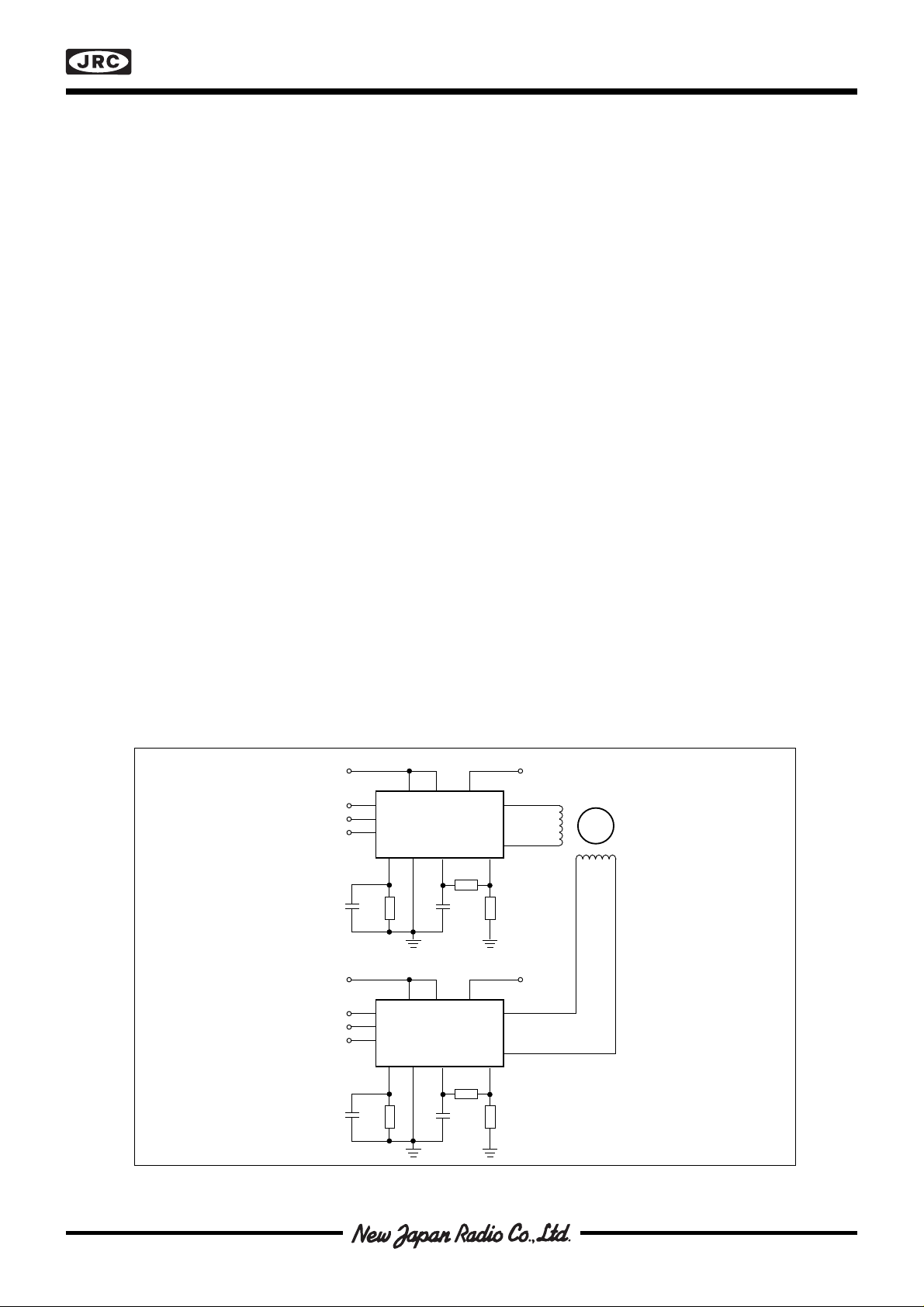
Figure 8. Typical stepper motor driver application with NJM3717
Page 9
NJM3717
16-pin
DIP
20-pin
EMP
28-pin
PLCC
Analog control
As the current levels can be continuously controlled by modulating the VR input, limited microstepping can be
achieved.
Switching frequency
The motor inductance, together with the pulse time, t
The choice of motor may then require other values on the RT , CT components than those recommended in figure7,
to obtain a switching frequency above the audible range. Switching frequencies above 40 kHz are not recommended because the current regulation can be affected.
Sensor resistor
The RS resistor should be of a non-inductive type, power resistor. A 1.0 ohm resistor, tolerance ≤ 1%, is a good
choice for 415 mA max motor current at VR = 5V.
The peak motor current, im , can be calculated by using the formulas:
im = (VR • 0.083) / RS [A], at 100% level
im = (VR • 0.050) / RS [A], at 60% level
im = (VR • 0.016) / RS [A], at 20% level
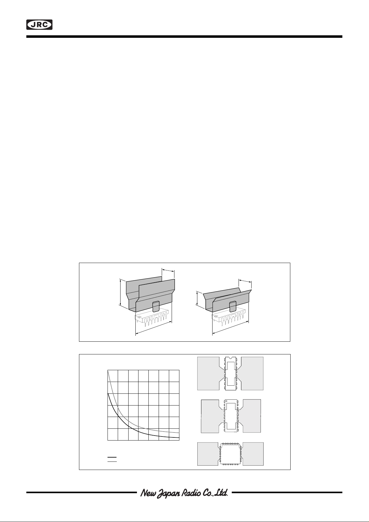
Heatsinking
The junction temperature of the chip highly effects the lifetime of the circuit. In high-current applications, the
heatsinking must be carefully considered.
The Rth
of the NJM3717 can be reduced by soldering the ground pins to a suitable copper ground plane on the
j-a
printed circuit board (see figure 10) or by applying an external heatsink type V7 or V8, see figure 9.
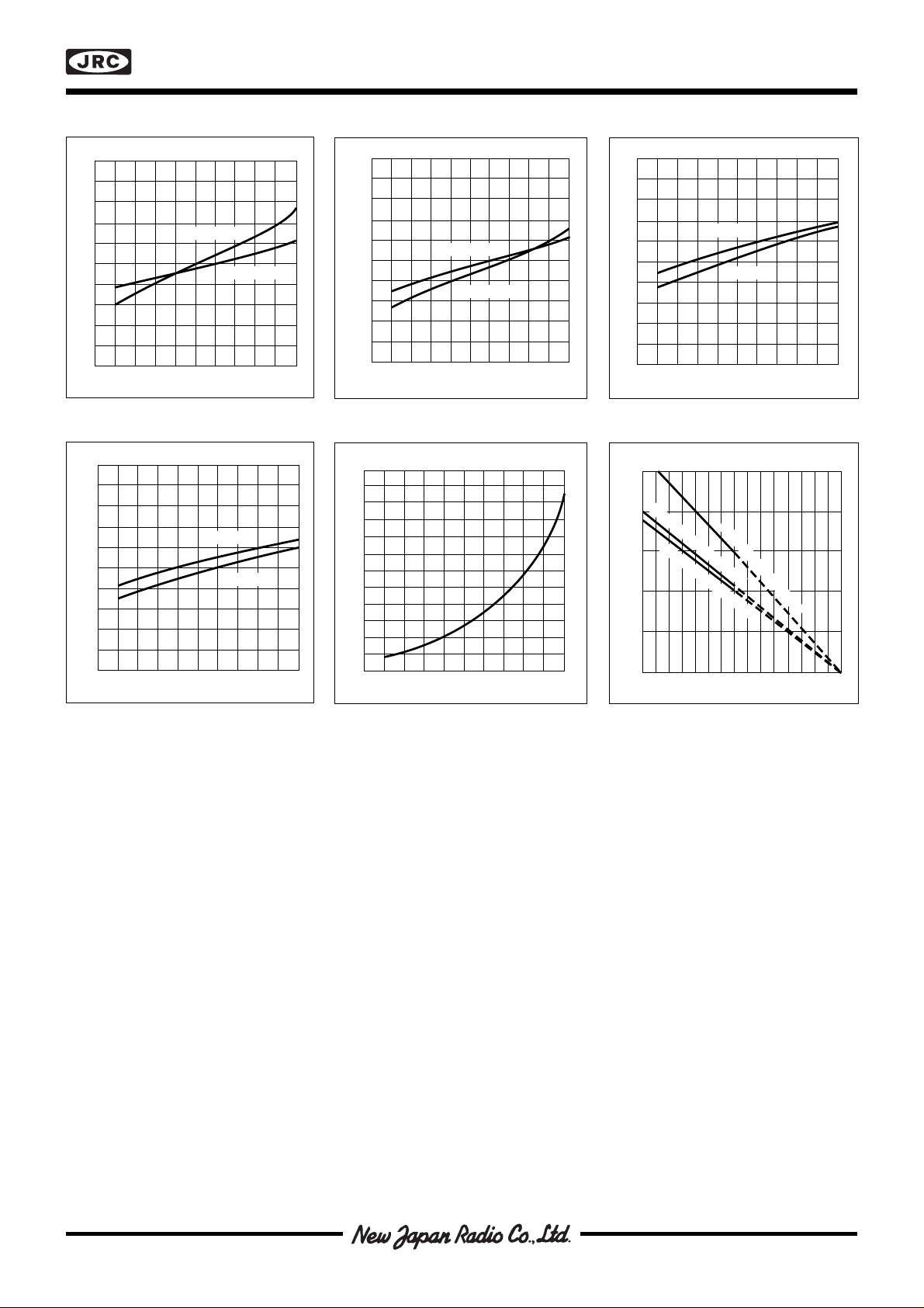
The diagram in figure 16 shows the maximum permissible power dissipation versus the ambient temperature in
°C, for heatsinks of the type V7, V8 or a 20 cm2 copper area respectively. Any external heatsink or printed circuit
board copper must be connected to electrical ground.
For motor currents higher than 500 mA, heatsinking is recommended to assure optimal reliability.
The diagrams in figures 9 and 10 can be used to determine the required heatsink of the circuit. In some systems,
forced-air cooling may be available to reduce the temperature rise of the circuit.
, determines the switching frequency of the current regulator.
off
3
3
,5
m
m
18,5 mm
38,5mm
11,6 mm
38.0 mm
38.0 mm
Figure 9. Heatsinks, Staver, type V7 and V8 by Columbia-Staver UK
Thermal resistance [°C/W]
90
80
70
60
50
40
30
5101520 303525
PCB copper foil area [cm ]
PLCC package
DIP and EMP package
2
Figure 10. Copper foil used as a heatsink
Page 10
■ TYPICAL CHARACTERISTICS
50 150
T
Amb
(°C)
0
2.0
4.0
3.0
1.0
PD (W)
100
With Staver V7 (27.5
°C/W)
With Staver V8 (37.5
°
C/W)
PC
B heatsink (40
°C/W)
V
(V)
Sat
1.8
1.6
1.4
1.2
1.0
.8
.6
.4
.2
0
0 .20 .40 .60 .80 1.0
IM (A)
Figure 11. Typical source saturation vs.
output current
T = 125
j
°C
Tj = 25°C
V
(V)
Sat
1.8
1.6
1.4
1.2
1.0
.8
.6
.4
.2
0
0 .20 .40 .60 .80 1.0
Tj = 25°C
T = 125
j
IM (A)
°C
Figure 12. Typical sink saturation vs.
output current
NJM3717
VF (V)
1.8
1.6
1.4
1.2
1.0
.8
.6
.4
.2
0
0 .20 .40 .60 .80 1.0
Figure 13. Typical lower diode voltage
drop vs. recirculating current
T = 25°C
j
Tj = 125°C
IM (A)
VF (V)
1.8
1.6
1.4
1.2
1.0
.8
.6
.4
.2
0
0 .20 .40 .60 .80 1.0
T = 25°C
IM (A)
j
Tj = 125°C
Figure 14. Typical upper diode voltage
drop vs. recirculating current
PD (W)
5
4
3
2
1
0
0 .20 .40 .60 .80 1.0
IM (A)
Figure 15. Typical power dissipation vs.
motor current
Figure 16. Allowable power dissipation
vs. ambient temperature
The specifications on this databook are only
given for information , without any guarantee
as regards either mistakes or omissions.
The application circuits in this databook are
described only to show representative
usages of the product and not intended for
the guarantee or permission of any right
including the industrial rights.
 Loading...