

Page 1
STEPPER MOTOR CONTROLLER / DRIVER
■ GENERAL DESCRIPTION ■ PACKAGE OUTLINE
NJM3517 is a stepper motor controller/driver, which requires
minimum of external components and drive currents up to 500mA.
The NJM3517 is suited for applications requiring least-possible RFI.
Operating in a bi-level drive mode can increase motor performance;
high voltage pulse is applied to the motor winding at the beginning
of a step, in order to give a rapid rise of current.
■ FEATURES
• Internal complete driver and phase logic
• Continuous-output current 2 x 350mA
• Half- and full-step mode generation
• LS-TTL-compatible inputs
• Bi-level drive mode for high step rates
NJM3517D2
NJM3517E2
NJM3517
• Voltage-doubling drive possibilities
• Half-step position-indication output
• Minimal RFI
• Packages DIP16 / EMP16
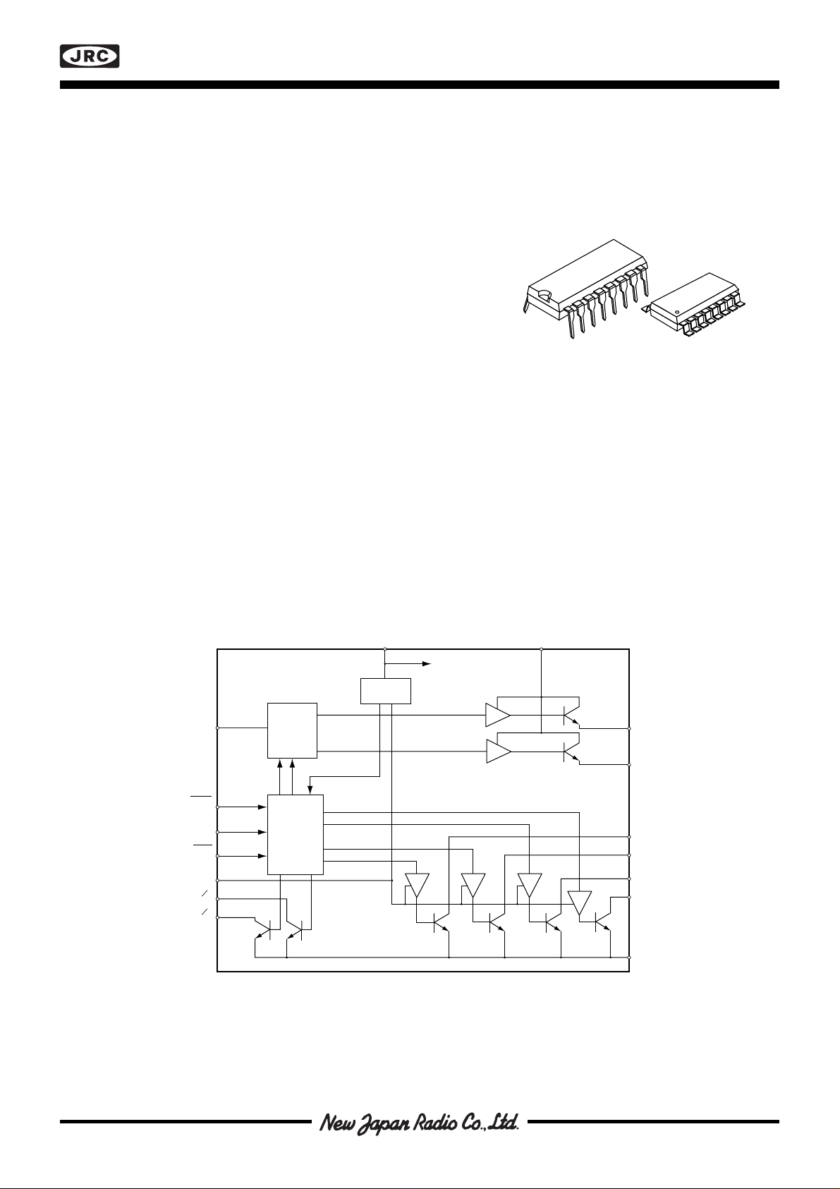
■ BLOCK DIAGRAM
NJM3517
RC
STEP
DIR
HSM
INH
O
OB
A
Mono
F - F
Phase
Logic
V
CC
POR
P
A
P
B
V
SS
L
A
L
B
P
B2
P
B1
P
A2
P
A1
Figure 1. Block diagram
GND
Page 2
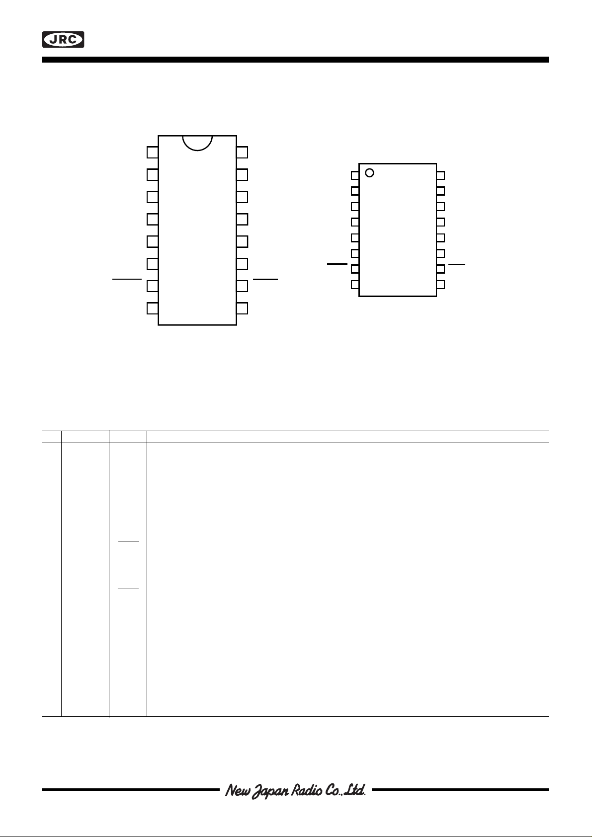
■ PIN CONFIGURATIONS
NJM3517
P
1
B2
P
2
B1
GND
STEP
P
A1
P
A2
DIR
Ø
3
4
5
NJM
3517D2
6
7
8
B
Fugure 2.Pin configurations
■ PIN DESCRIPTION
DIP EMP-pack. Symbol Description
16
15
14
13
12
11
10
9
V
CC
V
SS
L
B
L
A
R
C
INH
HSM
Ø
A
P
P
GND
P
P
DIR
STEP
Ø
1
B2
2
B1
3
NJM
4
A1
3517E2
5
A2
6
7
8
B
V
16
CC
15
V
SS
14
L
B
13
L
A
12
R
C
11
INH
10
HSM
9
Ø
A
11 PB2Phase output 2, phase B. Open collector output capable of sinking max 500 mA.
22 P
3 3 GND Ground and negative supply for both V
44 P
55 P
Phase output 1, phase B. Open collector output capable of sinking max 500 mA.
B1
and VSS.
CC
Phase output 1, phase A.
A1
Phase output 2, phase A.
A2
6 6 DIR Direction input. Determines in which rotational direction steps will be taken.
7 7 STEP Stepping pulse. One step is generated for each negative edge of the step signal.
8 8 ØB Zero current half step position indication output for phase B.
9 9 ØA Zero current half step position indication output for phase A.
10 10 HSM Half-step mode. Determines whether the motor will be operated in half or full-step
mot. When pulled low, one step pulse will correspond to a half step of the motor.
11 11 INH A high level on the inhibit input turns all phase output off.
12 12 RC Bi-level pulse timing pin. Pulse time is approximately t
= 0.55 • RT • C
on
T
13 13 LA Second level (bi-level) output, phase A.
14 14 LB Second level (bi-level) output, Phase B.
15 15 V
16 16 V
Second level supply voltage, +10 to +40 V.
SS
Logic supply voltage, nominally +5 V.
CC
Page 3
NJM3517
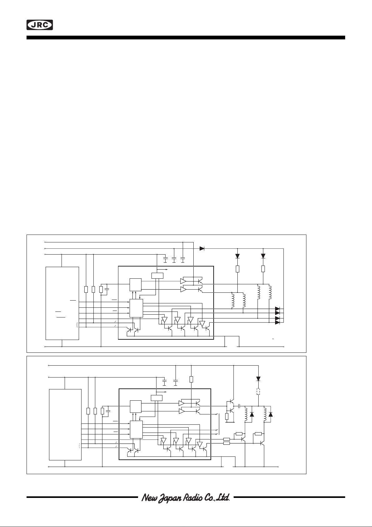
■ FUNCTIONAL DESCRIPTION
The circuit, NJM3517, is a high performance motor driver, intended to drive a stepper motor in a unipolar, bi-level
way. Bi-level means that during the first time after a phase shift, the voltage across the motor is increased to a
second voltage supply, VSS, in order to obtain a more-rapid rise of current, see figure 25.
The current starts to rise toward a value which is many times greater than the rated winding current. This com-
pensates for the loss in drive current and loss of torque due to the back emf of the motor.
After a short time, tOn, set by the monostable, the bi-level output is switched off and the winding current flows from
the VMM supply, which is chosen for rated winding current. How long this time must be to give any increase in
performance is determined by VSS voltage and motor data, the L/R time-constant.
In a low-voltage system, where high motor performance is needed, it is also possible to double the motor voltage
by adding a few external components, see figure 4.
The time the circuit applies the higher voltage to the motor is controlled by a monostable flip-flop and determined
by the timing components RT and CT.
The circuit can also drive a motor in traditional unipolar way.
An inhibit input (INH) is used to switch off the current completely.
■ LOGIC INPUTS
All inputs are LS-TTL compatible. If any of the logic inputs are left open, the circuit will accept it as a HIGH level.
NJM3517 contains all phase logic necessary to control the motor in a proper way.
STEP — Stepping pulse
One step is generated for each negative edge of the STEP signal. In half-step mode, two pulses will be required to
move one full step. Notice the set up time, ts, of DIR and HSM signals. These signals must be latched during the
negative edge of STEP, see timing diagram, figure 6.
V
SS
V
MM
+ 5V
CMOS, TTL-LS
Input / Output-Device
HALF / FULL STEP
NORMAL /INHIBIT
(Optional Sensor)
GND (V
CC
V
MM
+ 5V
CMOS, TTL-LS
Input / Output-Device
GND (V
V
CC
STEP
CW / CCW
GND
)
V
CC
STEP
CW / CCW
HALF / FULL STEP
NORMAL /INHIBIT
(Optional Sensor)
GND
)
CC
D3
+++
C3C4C
V
CC
16
PQR
RC 12
Mono
F - F
C
R
T
T
R9
R8
STEP 7
DIR 6
HSM 10
INH 11
9
O
A
OB 8
RC 12
C
R
T
T
R9
R8
STEP 7
DIR 6
HSM 10
INH 11
9
O
A
OB 8
Phase
Logic
Phase
Logic
Mono
F - F
P
A
P
B
C3C
V
CC
16
PQR
P
A
P
B
5
V
++
R1
4
V
SS
15
NJM3517
SS
15
13 L
A
14 L
B
1 P
B2
2 P
B1
5 P
A2
4 P
A1
3 GND
NJM3517
13 L
A
14 L
B
Equal to
1 P
B2
Phase A
2 P
B1
5 P
A2
4 P
A1
3 GND
Q1
Q3
R2
R4
R5
D2 D1
R11 R10
MOTOR
C1
+
1/2 MOTOR
R12 R13
Q5
D3-D6
D3-D6 are
UF 4001 or
BYV 27
trr < 100 ns
GND (VMM,VSS)
D1
R10
Q6
Figure 3.
Typical
application
Figure 4.
Voltage
doubling with
external
GND (V
MM,VSS
)
transistors
Page 4

NJM3517
DIR — Direction
DIR determines in which direction steps will be taken. Actual direction depends on motor and motor connections.
DIR can be changed at any time, but not simultaneously with STEP, see timing diagram, figure 6.
HSM determines whether the motor will be controlled in full-step or half-step mode. When pulled low, a steppulse will correspond to a half step of the motor. HSM can be changed at any time, but not simultaneously with
STEP, see timing diagram, figure 6.
INH — Inhibit
A HIGH level on the INH input,turns off all phase outputs to reduce current consumption.
■ RESET
An internal Power-On Reset circuit connected to Vcc resets the phase logic and inhibits the outputs during power
up, to prevent false stepping.
■ OUTPUT STAGES
The output stage consists of four open-collector transistors. The second high-voltage supply contains Darlington
transistors.
■ PHASE OUTPUT
The phase outputs are connected directly to the motor as shown in figure 3.
■ BI-LEVEL TECHNIQUE
The bi-level pulse generator consists of two monostables with a common RC network.
The internal phase logic generates a trigger pulse every time the phase changes state. The pulse triggers its own
monostable which turns on the output transistors for a precise period of time:
tOn = 0.55 • CT • RT.
See pulse diagrams, figures 7 through 11.
■ BIPOLAR PHASE LOGIC OUTPUT
The ØA and ØB outputs are generated from the phase logic and inform an external device if the A phase or the B
phase current is internally inhibited. These outputs are intended to support if it is legal to correctly go from a halfstep mode to a full-step mode without loosing positional information.
The NJM3517 can act as a controller IC for 2 driver ICs, the NJM3770A. Use PA1 and PB1 for phase control, and
ØA and ØB for I0 and I1 control of current turnoff.
Page 5

NJM3517
■ ABSOLUTE MAXIMUM RATINGS
Parameter Pin No. Symbol Min Max Unit
Voltage
Logic supply 16 V
Second suppl 15 V
Logic input 6, 7, 10, 11 V
Current
Phase output 1, 2, 4, 5 I
Second-level output 13, 14 I
Logic input 6, 7, 10, 11 I
The zero output 8, 9 I
Temperature
Operating junction temperature T
Storage temperature T
Power Dissipation (Package Data)
Power dissipation at Ta = 25°C, DIP package. Note 2. P
Power dissipation, EMP package. Note 3. P
CC
SS
I
P
L
I
Ο
j
Stg
D
D
07 V
045 V
-0.3 6 V
0 500 mA
-500 0 mA
-10 mA
-6 mA
-40 +150 °C
-55 +150 °C
- 1.6 W
- 1.3 W
■ RECOMMENDED OPERATING CONDITIONS
Parameter Symbol Min Typ Max Unit
Logic supply voltage V
Second-level supply voltage V
Phase output current I
Second-level output current I
Operating junction temperature T
Set up time t
Step pulse duration t
I
SS
I
CC
V
CC
16
POR
RC 12
Mono
F - F
V
SS
V
CC
V
I
V
IL
V
IH
IIIILI
STEP 7
DIR 6
HSM 10
IH
INH 11
9
O
A
OB 8
V
OCE Sat
Phase
Logic
P
A
P
B
NJM3517
V
SS
15
13 L
A
14 L
B
1 P
B2
2 P
B1
5 P
A2
4 P
A1
3 GND
CC
SS
P
L
J
s
p
V
LCE Sat
I
L
I
LL
IPI
PL
V
L
V
PCE Sat
V
P
4.75 5 5.25 V
10 - 40 V
0 - 350 mA
-350 - 0 mA
-20 - +125 °C
400 - - ns
800 - - ns
t
HSM
DIR
STEP
V
I
r
or
I
P
t
t
s
p
t
d
t
f
t
t
t
Figure 5. Definition of symbols
Figure 6. Timing diagram
Page 6

NJM3517
■ ELECTRICAL CHARACTERISTICS
Electrical characteristics at Tj = +25°C, VCC = +5.0 V, VMM = +40 V, VSS = +40 V unless otherwise specified.
Parameter Symbol Conditions Min Typ Max Unit
Supply current I
Phase outputs
Saturation voltage V
Leakage current I
Turn on, turn off t
Second-level outputs
Saturation voltage V
Leakage current I
On time t
Logic inputs
Voltage level, HIGH V
Voltage level, LOW V
Input current, LOW I
Input current, HIGH I
Logic outputs
Saturation voltage V
CC
PL
d
t
d
LL
On
IL
IH
PCE Sat
LCE Sat
IH
IL
ØCE Sat
INH = LOW - 45 60 mA
INH = HIGH - 12 - mA
IP = 350 mA - - 0.85 V
VP = 0 V - - 500 µA
+70°C--3µs
+125°C--6µs
IL = -350 mA - - 2.0 V
VL = 0 V -500 - - µA
(note 4) 220 260 300 µs
- 2.0 - V
- - 0.8 V
VI = 0.4 V -400 - - µA
VI = 2.4 V - - 20 µA
IØ = 1.6 mA - - 0.4 V
Notes
1. All voltages are with respect to ground. Current are positive into, negative out of specified terminal.
2 Derates at 12,8 mW/°C above +25°C.
3. Derates at 10.4 mW/°C above +25°C.
= 47 kΩ, CT = 10 nF.
4. R
T
Page 7

■ PURPOSE OF EXTERNAL COMPONENTS
For figures 3 and 4. Note that “Larger than …” is normally the vice versa of
“Smaller than … .”
Component Purpose Value Larger than value Smaller than value
D1, D2 Passes low power to
motor and prevents
high power from
shorting through low
power supply
D3 … D6 Inductive current
supressor
R1 Base drive current
limitter
R2, R3 Base discharge resistor R = 240ohm
R4 … R7 External transistor base
driver
R8, R9 ØA, ØB pull-up
resistors
R10, R11 Limit max. motor
current. Resistors may
be omitted. (Check
motor specifications
first.)
R12 … R15 External transistor base
discharge.
If = 1A
1N4001, UF4001
If = 1A
trr = 100nS
e.g. BYV27
UF4001
RGPP10G
RGPP30D
R = 20ohm
P = R1
P = R1
R =
P > (I4)2 • R4
Check hfe.
R = 5kohm @ pull-up
voltage = 5V.
P =
Vmm -V
R =
R =
P > Vbe • I
V
(
R1 + R
V
(
R1 + R
Vmm - Vbe - V
V
I4 -
(
R12
2
(VCC)
R
Motor
I
Motor max
V
be
15
=
I
12
12
mm
mm
be
Ω
Increases price Decreases max
Increases price Decreases current
Slows down turnoff time. Voltage
at anode might
exceed voltage
breakdown
Slows down Q1’s
2
turn-on and Q4’s
turn-off time.
)
2
Slows down Q1’s
2
turn-off and Q4’s
turn-on time.
)
2
CESat
Decreases ext.
transistor IC max.
Lowers 3517
power dissipation.
Increases noise
sensitivity, worse
logic-level
definition
Less stress on ØA,
ØB output
transistors
Decreases motor
current.
Slows down
external transistor
turn-off time.
Lowers 3517
power dissipation
ce
)
-V
NJM3517
current capability
turn-off capability
Speeds up turn-
off time.
Speeds up Q1’s
turn-on and Q4’s
turn-off time.
Speeds up Q1’s
turn-off and Q4’s
turn-on time.
Increases ext.
transistor IC max.
Increases 3517
power dissipation.
Increases noise
immunity, better
logic-level
definition.
Stress on ØA, ØB
output
transistors.
Increases motor
current.
Speeds up
external transistor
turn-off time.
Increases 3517
power dissipation
RT, CT Sets LA and LB on time
when triggered by
STEP.
C1, C2 Stores the doubling
voltage.
C3 … C5 Filtering of supply-
voltage ripple and takeup of energy feedback
from D3 … D6
Q1, Q2 Activation transistor of
voltage doubling.
Q3, Q4 Charging of voltage
doubling capacitor
Q5 … Q8 Motor current drive
transistor. PNP power trans.
R = 47kohm, C = 10nf
P < 250mW
C = 100µF
VC ≥ 45V
C µF Increases price,
10
≥
V
>Vmm,Vss or VccIncreases price Risk for capacitor
Rated
IC as motor requires. Increases price. Decreases max I
IC as motor requires.
Increases on time. Decreases on time.
Increases effective
on-time during
voltage doubling
better filtering,
decreases risk of
IC breakdown
(V
IC =
(
f
Step
Increases max
current capability.
- Vf -VCE) • C1
mm
1
- 0.55 • RT • C
Decreases
effective on-time
during voltage
doubling.
Decreases price,
more compact
solution.
breakdown.
during voltage
doubling.
T
)
Decreases max
current capability.
m
Page 8

DIR
DIR
INH
HSM
STEP
OB
LB
PB1
PB2
PA1
PA2
LA
OA
L
L
L
P
P
P
P
P
P
P
P
P
C
INH
HSM
STEP
OB
LB
PB1
PB2
PA1
PA2
LA
OA
NJM3517
H
L
H
P
L
P
P
P
P
P
P
L
DIR L
INT L
HSM H
STEP P
OB L
LB P
PB1 P
PB2 P
PA1 P
PA2 P
LA P
OA L
Figure 7. Full-step mode, forward. 4-step sequence. Gray-code
+90° phase shift.
DIR
H
INH
L
HSM
L
STEP
P
C
OB
P
LB
P
PB1
P
PB2
P
PA1
P
PA2
P
LA
P
OA
P
Figure 9. Half-step mode, forward. 8-step sequence.
DIR
L
INH
H
HSM
L
STEP
P
C
OB
P
LB
P
PB1
H
PB2
H
PA1
H
H
PA2
P
LA
P
OA
Figure 11. Half-step mode, inhibit.
Figure 8. Full-step mode, reverse. 4-step sequence. Graycode -90° phase shift.
Figure 10. Half-step mode, reverse. 8-step sequence.
■ APPLICATIONS INFORMATION
Logic inputs
If any of the logic inputs are left open, the circuit will treat it as a high-level input. Unused inputs should be connected to proper voltage levels in order to get the highest noise immunity.
Phase outputs
Phase outputs use a current-sinking method to drive the windings in a unipolar way. A common resistor in the
center tap will limit the maximum motor current.
Fast free-wheeling diodes must be used to protect output transistors from inductive spikes.
Series diodes in VMM supply, prevent VSS voltage from shorting through the VMM power supply. However, these
may be omitted if no bi-level is used. The VSS pin must not be connected to a lower voltage than VMM, but can be left
unconnected.
Zero outputs
ØA and ØB, “zero A” and “zero B,” are open-collector outputs, which go high when the corresponding phase output
is inhibited by the half-step-mode circuitry. A pull-up resistor should be used and connected to a suitable supply
voltage (5 kohms for 5V logic). See “Bipolar phase logic output.”
Interference
To avoid interference problems, a good idea is to route separate ground leads to each power supply, where the
only common point is at the NJM3517’s GND pin. Decoupling of VSS and VMM will improve performance. A 5 kohm
pull-up resistor at logic inputs will improve level definitions, especially when driven by open-collector outputs.
Page 9

NJM3517
R
Ext
V
i
R
Z
Figure 12. Diode turn-off circuit
Figure 15. Power return turn-off circuit
Figure 13. Resistance turn-off circuit
V
1
0V
Figure 16. Power return turn-off circuit
for bi-level
V
C
S
Power supply
2
Figure 14. Zener diode turn-off circuit
■ INPUT AND OUTPUT SIGNALS FOR DIFFERENT DRIVE MODES
The pulse diagrams, figures 7 through 10, show the necessary input signals and the resulting output signals for
each drive mode.
On the left side are the input and output signals, the next column shows the state of each signal at the cursor
position marked “C.”
STEP is shown with a 50% duty cycle, but can, of course, be with any duty cycle, as long as pulse time (tp) is
within specifications.
PA and PB are displayed with low level, showing current sinking.
LA and LB are displayed with high level, showing current sourcing.
■ USER HINTS
1. Never disconnect ICs or PC-boards when power is supplied.
2. If second supply is not used, disconnect and leave open VSS, LA, LB, and RC. Preferably replace the VMM supply
diodes (D1, D2) with a straight connection.
3. Remember that excessive voltages might be generated by the motor, even though clamping diodes are used.
4. Choice of motor. Choose a motor that is rated for the current you need to establish desired torque. A high
supply voltage will gain better stepping performance. If the motor is not specified for the VMM voltage, a current
limiting resistor will be necessary to connect in series with center tap. This changes the L/R time constant.
5. Never use LA or LB for continuous output at high currents. LA and LB on-time can be altered by changing the RC
net. An alternative is to trigger the mono-flip-flop by taking a STEP and then externally pulling the RC pin
(12Pin) low (0V) for the desired on-time.
6. Avoid VMM and VSS power supplies with serial diodes (without filter capacitor) and/or common ground with VCC.
The common place for ground should be as close as possible to the IC’s ground pin (pin 3).
Page 10

NJM3517
7. To change actual motor rotation direction, exchange motor connections at PA1 and PA2 (or PB1 and PB2).
8. Half-stepping. in the half-step mode, the power input to the motor alternates between one or two phase
windings. In half-step mode, motor resonances are reduced. In a two-phase motor, the electrical phase shift
between the windings is 90 degrees. The torque developed is the vector sum of the two windings energized.
Therefore, when only one winding is energized, which is the case in half-step mode for every second step, the
torque of the motor is reduced by approximately 30%. This causes a torque ripple.
9. Ramping. Every drive system has inertia which must be considered in the drive scheme. The rotor and load
inertia plays a big role at higher speeds. Unlike the DC motor, the stepper motor is a synchronous motor and
does not change speed due to load variations. Examination of typical stepper motors’ torque versus speed
curves indicates a sharp torque drop-off for the start-stop without error curve. The reason for this is that the
torque requirements increase by the cube of the speed change. As it can be seen, for good motor performance, controlled acceleration and deceleration should be considered.
■ COMMON FAULT CONDITIONS
•VMM supply not connected, or VMM supply not connected through diodes.
• The inhibit input not pulled low or floating. Inhibit is active high.
• A bipolar motor without a center tap is used. Exchange motor for unipolar version. Connect according to figure 3.
• External transistors connected without proper base-current supply resistor.
• Insufficient filtering capacitors used.
• Current restrictions exceeded.
•LA and LB used for continuous output at high currents. Use the RC network to set a proper duty cycle according
to specifications, see figures 19 through 24.
• A common ground wire is used for all three power supplies. If possible, use separate ground leads for each
supply to minimize power interference.
■ DRIVE CIRCUITS
If high performance is to be achieved from a stepper motor, the phase must be energized rapidly when turned on
and also de-energize rapidly when turned off. In other words, the phase current must increase/decrease rapidly at
phase shift.
■ PHASE TURN-OFF CONSIDERATIONS
When the winding current is turned off the induced high voltage spike will damage the drive circuits if not properly
suppressed. Different turn-off circuits
are used; e. g. :
Diode turn-off circuit (figure 12)
— Slow current decay
— Energy lost mainly in winding resistance
— Potential cooling problems.
Resistance T O C (figure 13)
— Somewhat faster current decay
— Energy lost mainly in R-Ext
— Potential cooling problems
Zener diode T O C (figure 14)
Relatively high VZ gives:
— Relatively fast current decay
— Energy lost mainly in V
— Potential cooling problems
Z
Page 11

■ TYPICAL CHARACTERISTICS
0.5
0.4
0.3
0.2
0.1
0
0 0.2 0.4 1.00.80.6
Output Current [A]
Output Voltage [V]
TA= +25° C
350
Motor Current [mA]
t
ON
Time
Normal
Bilevel
Bilevel without
time limit
NJM3517
V
sat [V]
LCE
2.5
TA= +25° C
2.0
1.5
1.0
0,5
0
0 0.1 0.2 0.50.40.3
I
[A]
L
Figure 17. Typical second output
saturation voltage vs. output current
Output Current [mA]
10
TA= +25° C
8
6
4
2
0
0 0.2 0.4 1.00.80.6
Output Voltage [V]
Allowable power dissipation [W]
2.5
2.0
1.5
1.0
0,5
0
0 50 100 150
Ambient temrature [°C]
Figure 18. Power dissipation vs. Ambient
temrature.
Output Pulse Width [s]
1
TA= +25° C
-1
10
-2
10
Rt = 100k
-3
10
-4
10
-5
10
-6
10
0.01 0.1 1 100010010
Ct Capacitance [nF]
Rt = 10M
Rt = 10k
Rt = 1k
Figure 19. Typical phase output satura-
tion voltage vs. output current
Output Pulse Width [s]
1
100%
-1
10
10%
-2
10
-3
10
-4
10
-5
10
-6
10
0.001 0.01 0.1 100101
1%
fs Step frequency [kHz]
TA= +25° C
Dutycykle
50%
25%
0.1%
Figure 20. Typical IØ vs. V
output” saturation
Output Current [A]
0.5
TA= +25° C
0.4
0.3
0.2
0.1
0
0 0.2 0.4 1.00.80.6
ØCE Sat
(I
. “Zero
L= 0)
Power Dissipation [W]
Figure 23. Typical P
dissipation without second-level supply
vs. IP. Power
DP
(includes 2 active outputs = FULL STEP)
Figure 21. Typical t
pulse width vs. capacitance/resistance
Output Current [A]
-0.5
TA= +25° C
-0.4
10% 50% 100%
-0.3
-0.2
-0.1
0
0 0.2 0.4 1.00.80.6
vs. CT/RT. Output
On
(Ip = 0)
Power Dissipation [W]
Figure 24. Typical PDL vs. IL. Power
dissipation in the bilevel pulse when
raising to the I
value. One active output
L
Figure 22.Typical t
vs. fs/dc. Output
on
pulse width vs.step frequency/duty
Figure 25 . Motor Current IP
Page 12

NJM3517
Power return T O C for unipolar drive (figure 15)
Relatively high VZ gives:
— Relatively fast current decay
— Energy returned to power supply
— Only small energy losses
— Winding leakage flux must be considered
— Potential cooling problems
Power return to T O C for bi-level drive (figure 16)
— Very fast current decay
— Energy returned to power supply
— Only small energy losses
— Winding leakage flux must be considered
■ DIAGRAMS
How to use the diagrams:
1. What is the maximum motor current in the application?
• The ambient temperature sets the maximum allowable power dissipation in the IC, which relates to the
motor currents and the duty cycle of the Bi-level function. For NJM3517, without any measures taken to
reduce the chip temperature via heatsinks, the power dissipation vs. temperature follows the curve in figure
18.
• Figures 23 and 24 give the relationship between motor currents and their dissipations. The sum of these
power dissipations must never exceed the previously-established value, or life expectancy will be drastically
shortened.
• When no Bi-level or voltage doubling is utilized, the maximum motor current can be found directly in figure
23 .
2. How to choose timing components.
• Figure 21 shows the relationship between CT, RT, and tOn. Care must be taken to keep the tOn time short,
otherwise the current in the winding will rise to a value many times the rated current, causing an overheated
IC or motor.
3. What is the maximum tOn pulse-width at a given frequency?
• Figure 22 shows the relationship between duty cycle, pulse width, and step frequency. Check specifications
for the valid operating area.
4. Figures 17, 18 and 20 show typical saturation voltages vs. output current levels for different output transistors.
5. Shaded areas represent operating conditions outside the safe operating area.
The specifications on this databook are only
given for information , without any guarantee
as regards either mistakes or omissions. The
application circuits in this databook are
described only to show representative usages
of the product and not intended for the
guarantee or permission of any right including
the industrial rights.
 Loading...