

Page 1
NJM2575
LOW VOLTAGE VIDEO AMPLIFIER WITH LPF
■GENERA L DESCRIPTION ■PACKAGE OUTLINE
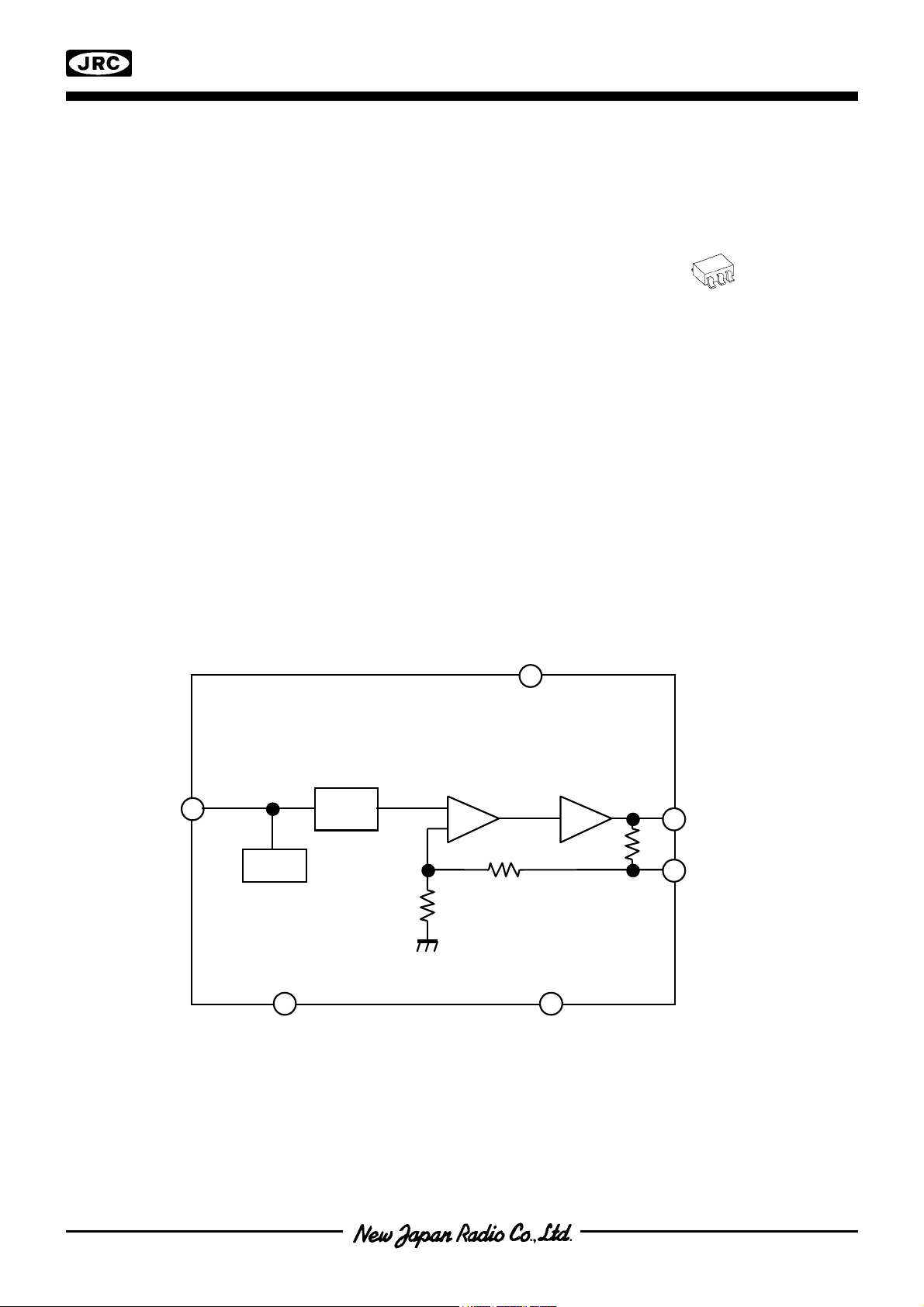
The NJM2575 is a Low Voltage Video Amplifier contained LPF circuit,
75Ω driver to connect TV monitor directly.
The mute circuit with power save function is suitable for low power
design. The NJM2575 is suitable for down
■FEATURES
●Operating Voltage 2.8 to 5.5V
●Input Composite Video Signal 1.0Vpp
●Internal Low Pass Filter
●Operating Current 7.0mA typ. at Vcc=3.0V
●Operating Current Power Save Mode 60uA typ.at Vcc=3.0V
●Bipolar Technology
●Package Outline MTP6
■BLOCK DIA G RA M
6dB
4
Vin
CLAMP
5
LPF
+
V
6
Power SaveGND
75Ω
1
Driver
NJM2575F1
2
3
Vout
Vsag
-1 -
Page 2
NJM2575
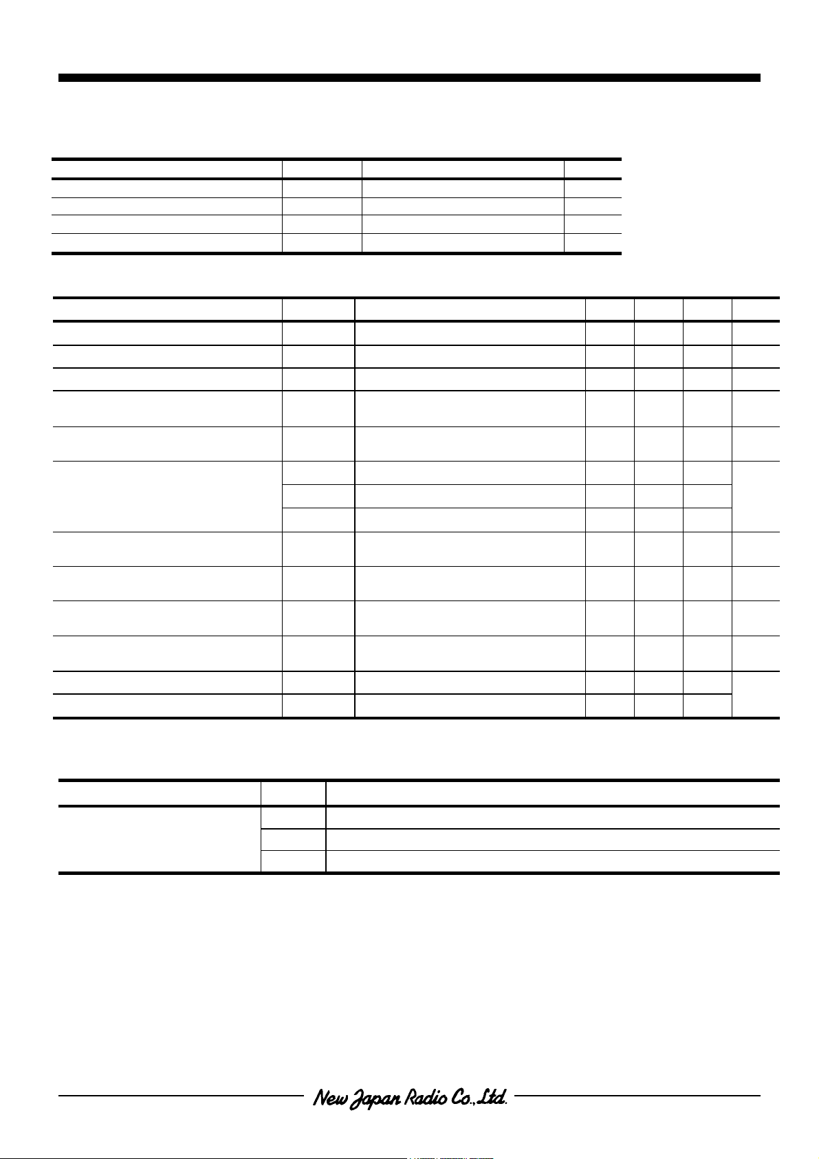
■ABSOLUTE MAXIMUM RATINGS (Ta=25°C)
PARAMETER SYMBOL RATINGS UNIT
Supply Voltage V+ 7.0 V
Power Dissipation PD 200 mW
Operating Temperature Range Topr -40 to +85
Storage Temperature Range Tstg -40 to +125
°C
°C
■ELECTRICAL CHARACTERISTICS ( V
+
=3.0V,R
=150Ω,Ta=25°C)
L
PARAMETER SYMBOL TEST CONDITION MIN. TYP. MAX. UNIT
Operating Voltage Vopr 2.8 3.0 5.5 V
Operating Current ICC No Signal - 7.0 10.0 mA
Operating Current at Power Save Isave Power Save Mode - 60 90 uA
Maximum Output Voltage Swing Vom f=1kHz,THD=1% 2.2 2.4 - Vp-p
Voltage Gain Gv
Vin=100kHz,1.0Vp-p,
Input Sine Signal
6.1 6.5 6.9 dB
Gfy4.5M Vin=4.5MHz/100kHz,1.0Vp-p -0.5 0.0 +0.5
Low Pass Filter Characteristic
Gfy8M Vin=8MHz/100kHz,1.0Vp-p - -2.0 -
Gfy16M Vin=16MHz/100kHz,1.0Vp-p - -12.0 -
Differential Gain DG
Differential Phase DP
S/N Ratio SNv
2nd. Distortion Hv
Vin=1.0Vp-p,
Input 10step Video Signal
Vin=1.0Vp-p,
Input 10step Video Signal
Vin=1.0Vp-p,
100% White Video Signal, R
Vin=1.0Vp-p,3.58MHz,
Sine Video Signal, R
=75Ω
L
=75Ω
L
- 0.2 - %
- 0.2 - deg
- +60 - dB
- -40 - dB
SW Change Voltage High Level VthPH active 1.8 - V+
SW Change Voltage Low Level VthPL non-active 0 - 0.3
■CONTROL TER MI NA L
PARAMETER STATUS NOTE
H Power Save : OFF
Power Save
L Power Save : ON
OPEN Power Save : ON
- 2 -
dB
V
Page 3
3
654
3
2
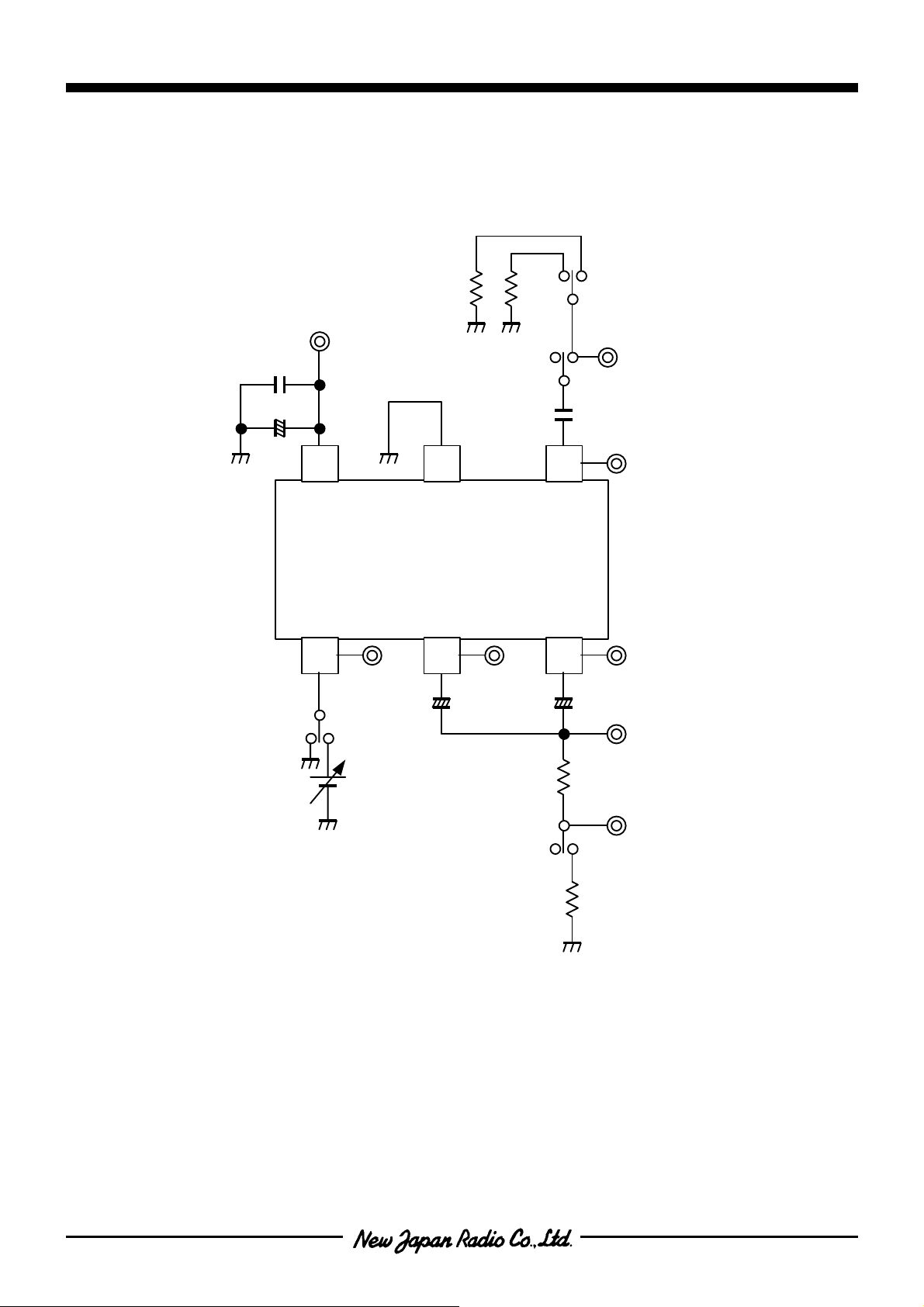
■TEST CIR CUIT
NJM2575
75Ω 50Ω
0.1uF
10uF
+
+
V
Power
Save
1
open
GND Vin
NJM2575
+
input
0.1uF
VsagVout
+
22uF100uF
output
75Ω
open
75Ω
-
-
Page 4
654
3
2
654
3
2
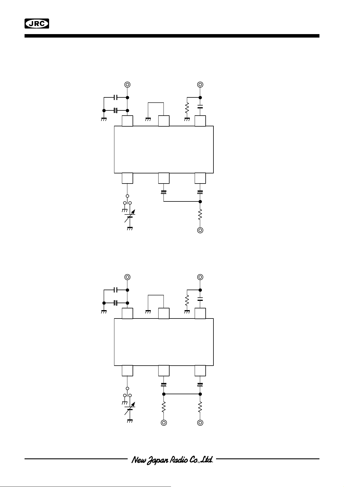
■APPLICATION CIRCUIT
0.1uF
NJM2575
+
V
input
10uF
75Ω
+
+
V
GND Vin
0.1uF
NJM2575
Power
Save
1
+
+
V
VsagVout
+
output
input
33uF33uF
75Ω
0.1uF
10uF
+
75Ω
+
V
GND Vin
0.1uF
NJM2575
Power
Save
1
+
75Ω
output2
75Ω 2System Drive
VsagVout
+
75Ω
output1
33uF100uF
-4 -
Page 5
5
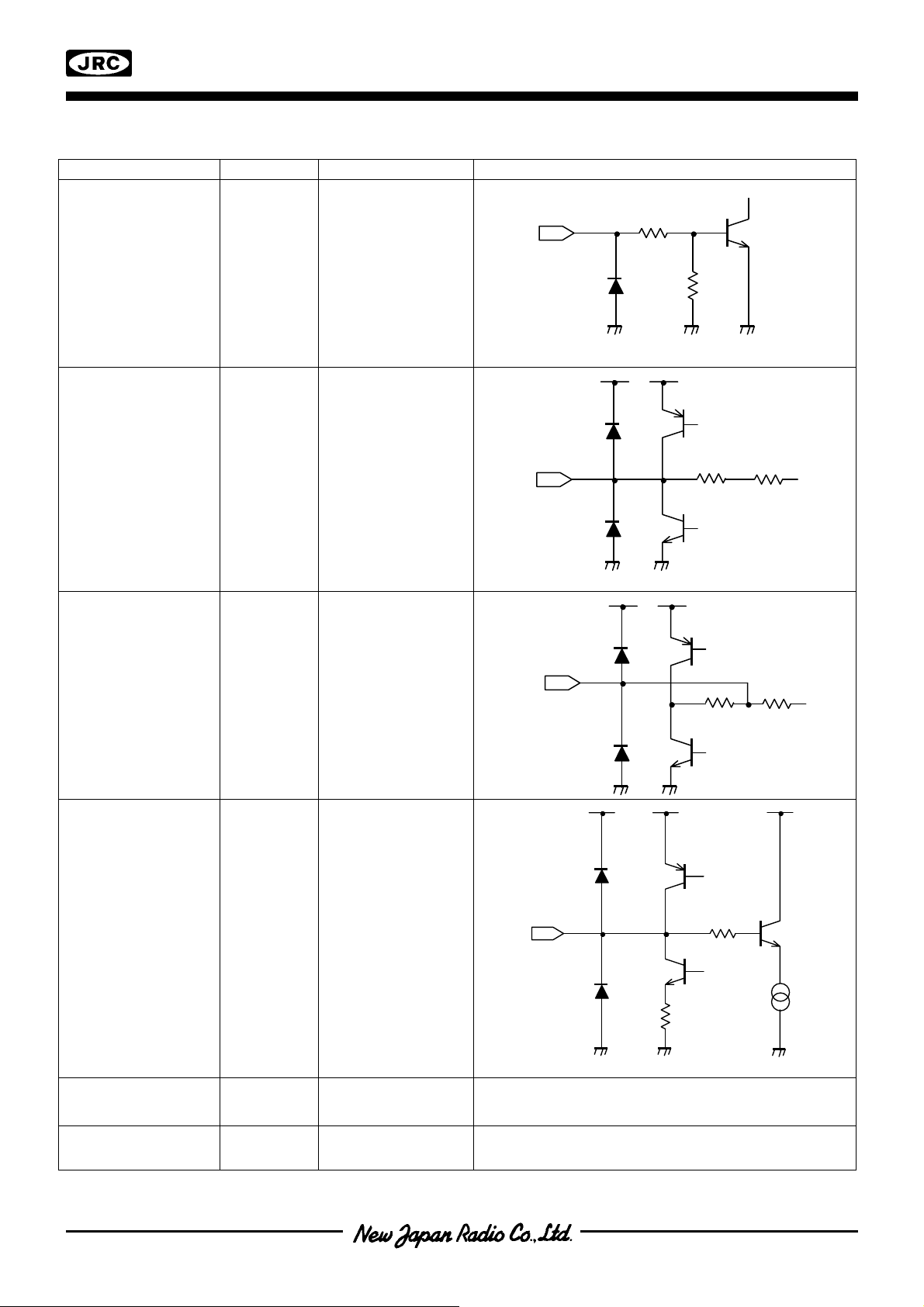
■TERMINA L FUNCTION
PIN No. PIN NAME DC VOLTAGE EQUIVALENT CIRCUIT
Power
1
Power
save
save
-
32KΩ
NJM2575
48KΩ
2 Vout 0.26V
Vout
3 Vsag -
Vsag
+
V
V
+
V
750Ω 25.3KΩ
+
+
V
750Ω 25.3KΩ
+
V
+
V
+
V
4 Vin 1.10V
Vin
5 GND -
6 V+ 3V
-
-
Page 6
NJM2575
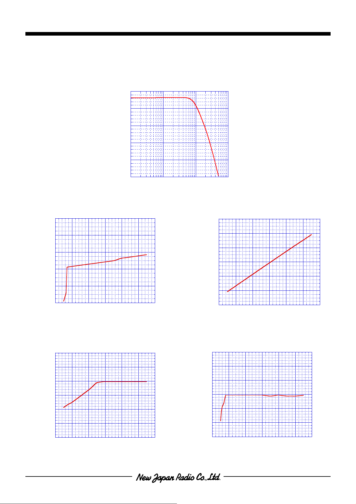
■■■■TYPICAL CHARACTERISTI CS
Frequency Characteristic
10
0.0
-10
Gain (dB)
-20
-30
-40
5
10
6
10
Frequency (Hz)
7
10
8
10
Operating Current vs. Supply Voltage
12
10
8
6
Operating Current Icc(mA)
4
2
2345678
Supply Voltage V+(V)
Maximum Output Voltage Swing vs. Supply Voltage
6
5
4
Operating Curr ent at Standby State vs. Supply Voltage
120
100
80
60
40
20
Operating Cur rent at St andby State Isave(uA)
0
2345678
Supply Voltage V+(V)
Voltage Gain vs. Supply Voltage
8
7.5
7
- 6 -
3
2
1
Maximum Output Voltage Swing Vom(Vpp)
0
2345678
Supply Voltage V+(V)
6.5
6
Voltage Gain Gv(dB)
5.5
5
2345678
Supply Voltage V+(V)
Page 7
■■■■TYPICAL CHARACTERISTI CS
NJM2575
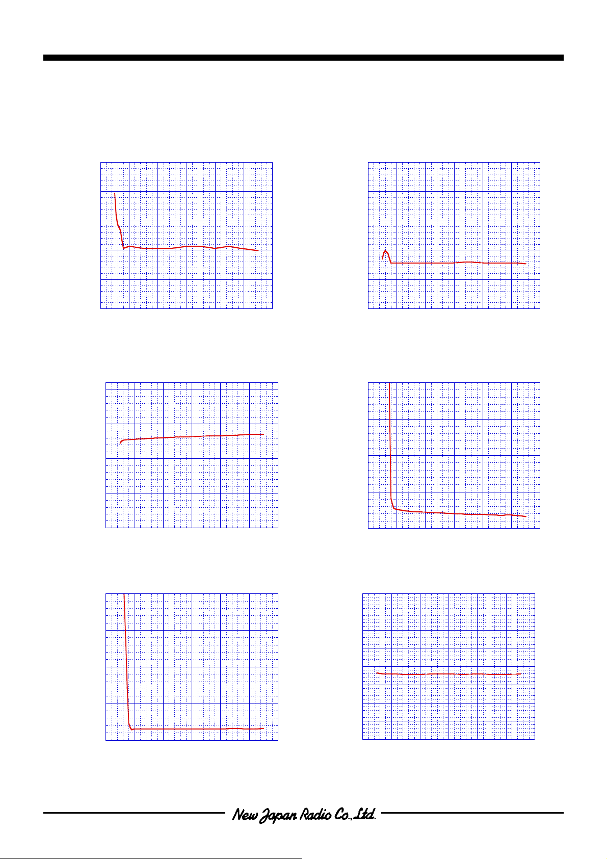
Low Pass Filter Characteristic1 vs. Supply Voltage
1.5
1
0.5
0
LPF Characteristic1 Gfy4.5M (dB)
-0.5
-1
2345678
Low Pass Filte r Ch ara c teristic3 vs. Suppl y Volta ge
-5
-10
(Vin=4.5MHz/100kHz)
LPF Characteristic2 Gfy8M(dB)
Supply Voltage V+(V)
(Vin=16MHz/100kHz)
Low Pass Filt e r Ch ara cteristic2 vs. S upply Voltage
2
1
0
-1
-2
-3
2345678
2
1.5
(Vin=8MHz/100kHz)
Supply Voltage V+(V)
Differential Gain vs. Supply Voltage
-15
LPF Characteristic3 Gfy16M(d B)
-20
-25
2345678
Supply Voltage V+(V)
2
1.5
1
Differential Phase DP(deg)
0.5
0
Differenti al Phase vs. Supply Volta ge
Signal to Noise Ratio SNv(dB)
2345678
Supply Voltage V+(V)
1
Differential Gain DG(%)
0.5
0
2345678
Supply Voltage V+(V)
Signal to Noise Ratio vs. Supply Voltage
90
85
80
75
70
65
60
55
50
2345678
Supply Voltage V+(V)
-7 -
Page 8
NJM2575
■■■■TYPICAL CHARACTERISTI CS
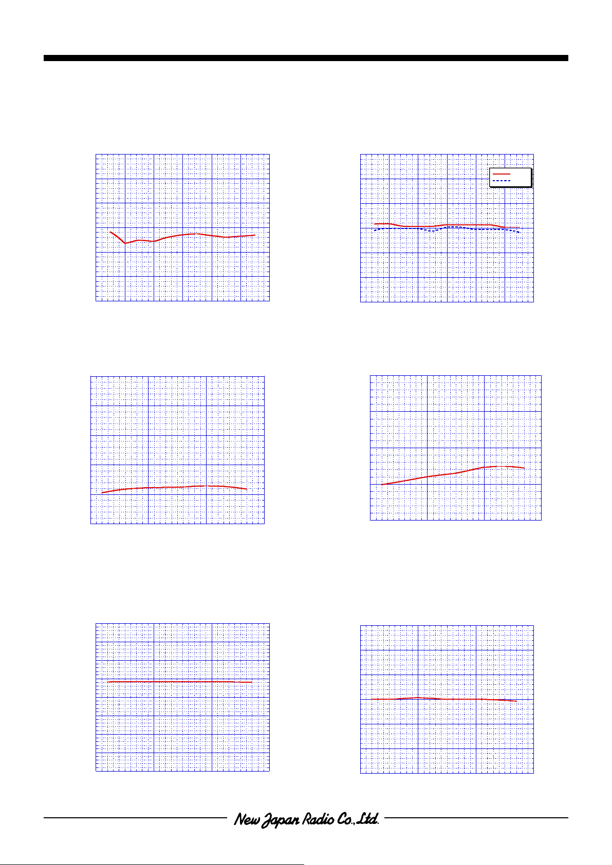
Second Harmonic Distortion vs. Supply Volta ge
-20
-30
-40
-50
-60
Second Harmonic D istortion Hv(dB)
-70
-80
2345678
Supply Voltage V+(V)
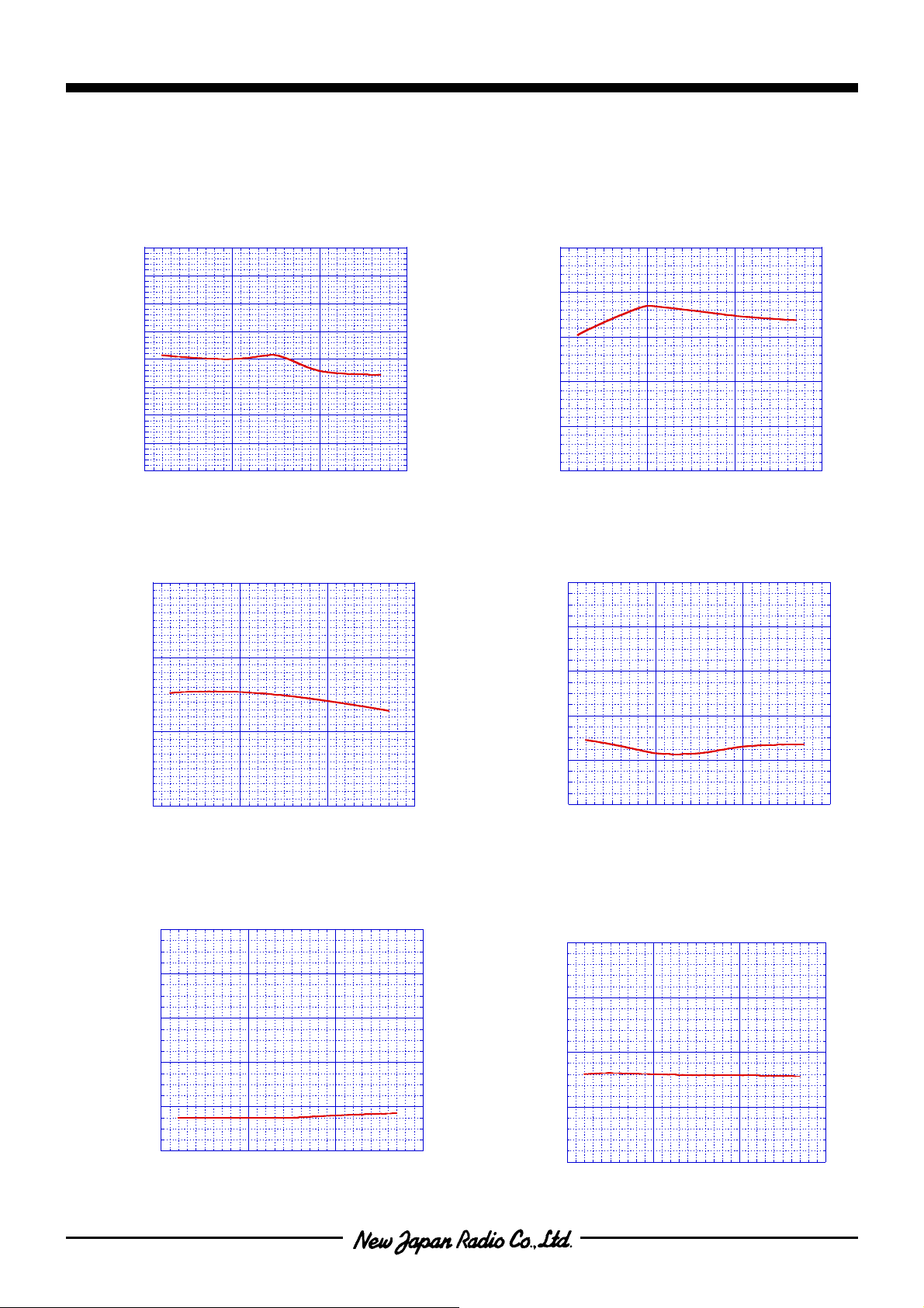
Operating Current vs. Temperature
10
9
8
7
1.4
1.3
1.2
1.1
1
Switching Voltage Vth(V)
0.9
0.8
Switching Voltage vs. Supply Voltage
VthPH
VthPL
2345678
Supply Voltage V+(V)
Operating Current at Standby State vs. Temperature
40
35
30
- 8 -
Operationg Current Icc(mA)
6
5
-50 0 50 100
Ambient Temperature Ta (oC)
Maximum Outp ut Voltage Swing vs. Temperature
4
3.5
3
2.5
2
1.5
1
Maximum Output Voltage Swing Vom(Vpp)
0.5
0
-50 0 50 100
Ambient Temperature Ta (oC)
25
Operating Current at Standby State Isave(uA)
20
-50 0 50 100
Ambient Temperature Ta (oC)
Voltage Gain vs. Temperature
8
7.5
7
6.5
Voltage Gain Gv(dB)
6
5.5
5
-50 0 50 100
Ambient Temperature Ta(oC)
Page 9
9
■■■■TYPICAL CHARACTERISTI CS
NJM2575
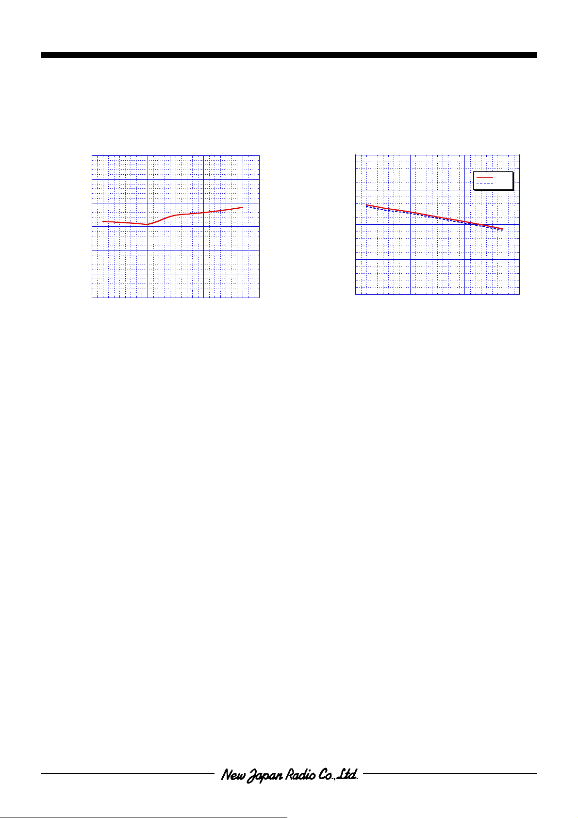
Low Pass Filt e r Ch aracteristic 1 vs. Temperature
2
1.5
1
0.5
0
-0.5
-1
LPF Characteristic 1 Gfy4.5M(dB)
-1.5
-2
-50 0 50 100
Low Pass Filte r Characteristic 3 vs. Temperature
-5
-10
(Vin=4.5MHz/100kHz)
Ambient Temperature Ta(oC)
(Vin=16MHz/100kHz)
Low Pass Filte r Characteristic 2 vs. Temperature
0
-1
-2
-3
LPF Characteristic 2 Gfy8M(dB)
-4
-5
-50 0 50 100
1
0.8
0.6
(Vin=8MHz/100kHz)
Ambient Temperature Ta(oC)
Differential Gain vs. Temperature
0.4
-15
LPF Characteristic 3 Gfy16M(dB)
-20
-50 0 50 100
Ambient Temperature Ta(oC)
Differential Gain DG(%)
0.2
0
-50 0 50 100
Ambient Temperature Ta(oC)
Differential Phase vs. Temperature
1
0.8
0.6
0.4
Differential Phase DP(deg)
0.2
0
-50 0 50 100
Ambient Temperature Ta(oC)
80
75
70
Signal to Noise Ratio SNv(dB)
65
60
Signal to Noise Ratio vs. Temperature
-50 0 50 100
Ambient Temperature Ta (oC)
-
-
Page 10
NJM2575
■■■■TYPICAL CHARACTERISTI CS
Second Harmonic Distortion vs. Temperature
-40
-45
-50
-55
-60
Second Harmonic Distortion Hv(dB)
-65
-70
-50 0 50 100
Ambient Temperature Ta (oC)
2
1.5
1
Switching Volt age Vth(V)
0.5
0
-50 0 50 100
Switching V oltage vs. Temperature
Ambient Temperature Ta(oC)
VthPH
VthPL
- 10 -
Page 11
NJM2575
■■■■ APPLICATION
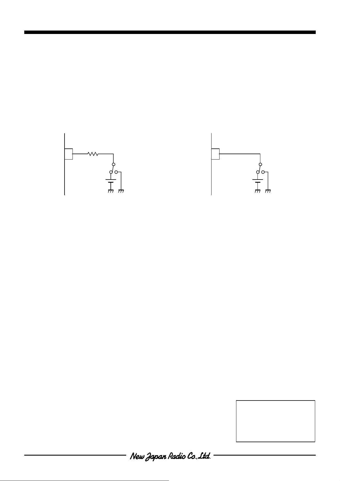
When you use a power save terminal more than by 4.0V, please put resistance of about 20kΩ into a power
save terminal.
I n addition, power save terminal voltage (VthH) -- in the case of below 4.0V, resistance is not required
Example)
● PS(VthH) ≥ 4.0V ● PS(VthH) < 4.0V
V
PS
(VthH)
r
VthH
r ≅ 20k
4.0V
≥
Ω
Power
Save
VthH < 4.0V
VPS(VthH)
Power
Save
[CAUTION]
The specifications on this databook are only
given for information , without any guarantee
as regards either mistakes or omissions. The
application circuits in this databook are
described only to show representative usages
of the product and not intended for the
guarantee or permission of any right including
the industrial rights.
- 11 -
 Loading...