

Page 1
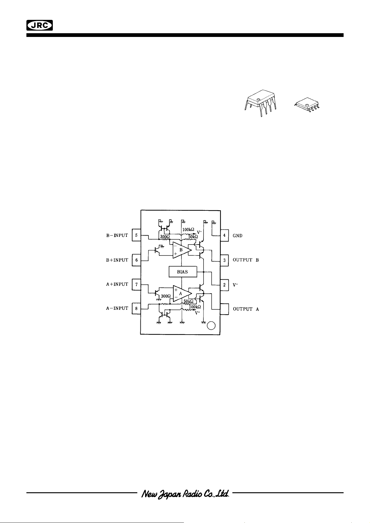
DUAL LOW VOLTAGE POWER AMPLIFIER
■ GENERAL DESCRIPTION ■ PACKAGE OUTLINE
The NJM2073 is a monolithic integrated circuit in 8 lead
dual-in-line package,which is designed for dual audio power
amplifier in portable radio and handy cassette player.
■ FEATURES
● Operating Voltage ( V+=1.8V~15V )
● Low Crossover Distortion
● Low Operating Current
● Bridge or Stereo Configuration
● No Turn-on Noise
● Package Outline DIP8,DMP8
● Bipolar Technology
■ PIN CONFIGURATION
NJM2073D
NJM2073M
NJM2073D
NJM2073
NJM2073M
Ver.2004-03-01
-
-
Page 2
NJM2073
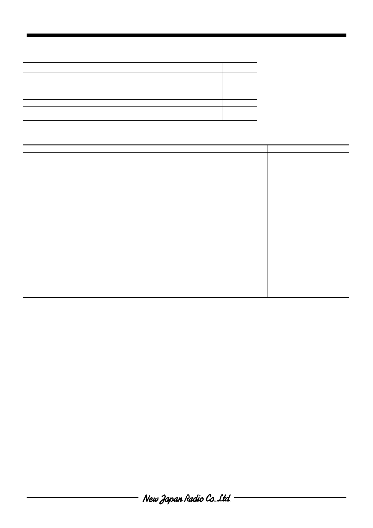
■ ABSOLUTE MAXIMUM RATINGS
( Ta=25˚C )
PARAMETER SYMBOL RATINGS UNIT
Supply Voltage V+ 15 V
Output Peak Current IOP 1 A
Power Dissipation PD
( DIP8 ) 700
( DMP8 ) 300
mW
Input Voltage Range VIN ± 0.4 V
Operating Temperature Range T
Storage Temperature Range T
-40~+85 ˚C
opr
-40~+125 ˚C
stg
■ ELECTRICAL CHARACTERISTICS D-Type
(1) BTL Configuration ( Test Circuit Fig.1 ) ( V
PARAMETER SYMBOL TEST CONDITION MIN. TYP. MAX. UNIT
Operating Voltage V+ 1.8 - 15 V
Operating Current ICC R
=∞ - 6 9 mA
L
Output Offset Voltage ∆VO RL=8Ω - 10 50 mV
( Between the Outputs )
Input Bias Current IB - 100 - nA
Output Power
P
P
P
P
P
P
O
O
O
O
O
O
P
P
O
O
THD=10%,f=1kHz
V
V
V
V
V
V
V
V
+
=9V,RL=16Ω ( Note ) - 2.0 - W
+
=6V,RL=8Ω ( Note ) 0.9 1.2 - W
+
=4.5V,RL=8Ω - 0.6 - W
+
=4.5V,RL=4Ω ( Note ) - 0.8 - W
+
=3V,RL=4Ω 200 300 - mW
+
=2V,RL=4Ω - 80 - mW
THD=1%,f=40Hz~15kHz
+
=6V,RL=8Ω - 1.0 - W
+
=4.5V,RL=4Ω - 0.6 - W
Total Harmonic Distortion THD PO=0.5W,RL=8Ω,f=1kHz - 0.2 Close Loop Voltage Gain AV f=1kHz 41 44 47 dB
Input Impedance ZIN f=1kHz 100 - - kΩ
Equivalent Input Noise Voltage V
V
R
NI1
R
NI2
=10kΩ,A Curve - 2 - µV
S
=10kΩ,B=22Hz~22kHz - 2.5 - µV
S
Ripple Rejection RR f=100Hz - 40 - dB
Cutoff Frequency fH A
( Note ) At on PC Board
=-3dB from f=1kHz,RL=8Ω,PO=1W - 130 - kHz
V
+
=6V,Ta=25˚C )
%
-
-
Ver.2004-03-01
Page 3
NJM2073
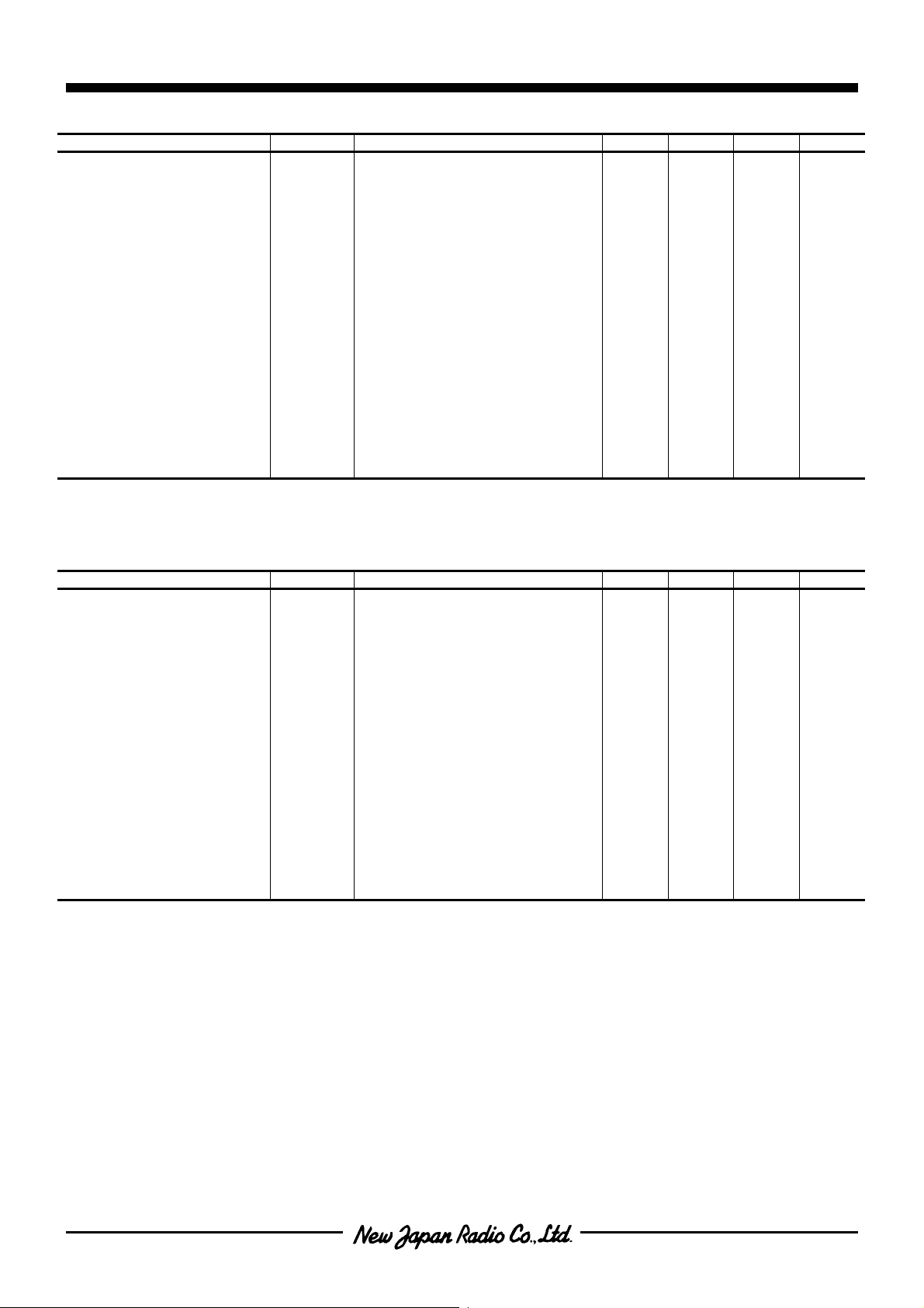
(2) Stereo Configuration ( Test Circuit Fig.2 )
PARAMETER SYMBOL TEST CONDITION MIN. TYP. MAX. UNIT
Operating Voltage V+ 1.8 - 15 V
Output Voltage VO - 2.7 - V
Operating Current ICC R
Input Bias Current IB - 100 - nA
Output Power ( Each Channel )
P
P
P
P
P
P
V
O
V
O
V
O
V
O
V
O
V
O
Total Harmonic Distortion THD PO=0.4W,RL=4Ω,f=1kHz - 0.25 Voltage Gain AV f=1kHz 41 44 47 dB
Channel Balance ∆AV - - ± 1 dB
Input Impedance ZIN f=1kHz 100 - - kΩ
Equivalent Input Noise Voltage V
V
R
NI1
R
NI2
Ripple Rejection RR f=100Hz,CX=100µF 24 30 - dB
Cutoff Frequency fH A
( Note ) At on PC Board
■ ELECTRICAL CHARACTERISTICS M-Type
(1) BTL Configuration ( Test Circuit Fig.1 ) ( V
PARAMETER SYMBOL TEST CONDITION MIN. TYP. MAX. UNIT
Operating Voltage V+ 1.8 - 15 V
Operating Current ICC R
Output Offset Voltage ∆VO RL=8Ω - 10 50 mV
( Between the Outputs )
Input Bias Current IB - 100 - nA
Output Power
P
P
P
P
P
V
O
V
O
V
O
V
O
V
O
Total Harmonic Distortion THD V+=4V,RL=8Ω,PO=200mW,f=1kHz - 0.2 Close Loop Voltage Gain AV f=1kHz 41 44 47 dB
Input Impedance ZIN f=1kHz 100 - - kΩ
Equivalent Input Noise Voltage V
V
R
NI1
R
NI2
Ripple Rejection RR f=100Hz - 40 - dB
Cutoff Frequency fH A
( Note ) At on PC Board
=∞ - 6 9 mA
L
THD=10%,f=1kHz
+
=6V,RL=4Ω ( Note ) 0.5 0.65 - W
+
=4.5V,RL=4Ω - 0.32 - W
+
=3V,RL=4Ω - 120 - mW
+
=2V,RL=4Ω
THD=1%,f=1kHz
+
=6V,RL=4Ω - 500 - mW
+
=4.5V,RL=4Ω - 250 - mW
- 30 - mW
%
=10kΩ,A Curve - 2.5 - µV
S
=10kΩ,B=22Hz~22kHz - 3 - µV
S
=-3dB from f=1kHz,RL=8Ω,PO=250mW - 200 - kHz
V
+
=6V,Ta=25˚C )
=∞ - 6 9 mA
L
THD=10%,f=1kHz
+
=6V,RL=16Ω ( Note ) - 0.8 - W
+
=4V,RL=8Ω ( Note ) 350 460 - mW
+
=3V,RL=4Ω ( Note ) 200 300 - mW
+
=2V,RL=4Ω
THD=1%,f=40Hz~15kHz
+
=4V,RL=8Ω - 380 - mW
- 80 - mW
%
=10kΩ,A Curve - 2 - µV
S
=10kΩ,B=22Hz~22kHz - 2.5 - µV
S
=-3dB from f=1kHz,RL=16Ω,PO=0.5W - 130 - kHz
V
Ver.2004-03-01
-
-
Page 4
NJM2073
(2) Stereo Configuration ( Test Circuit Fig.2 )
PARAMETER SYMBOL TEST CONDITION MIN. TYP. MAX. UNIT
Operating Voltage V+ 1.8 - 15 V
Output Voltage VO - 2.7 - V
Operating Current ICC R
Input Bias Current IB - 100 - nA
Output Power ( Each Channel )
P
P
P
P
P
P
V
O
V
O
V
O
V
O
V
O
V
O
Total Harmonic Distortion THD V+=4V,RL=4Ω,PO=150mW,f=1kHz - 0.25 Voltage Gain AV f=1kHz 41 44 47 dB
Channel Balance ∆AV - - ± 1 dB
Input Impedance ZIN f=1kHz 100 - - kΩ
Equivalent Input Noise Voltage V
V
R
NI1
R
NI2
Ripple Rejection RR f=100Hz,CX=100µF 24 30 - dB
Cutoff Frequency fH A
( Note ) At on PC Board
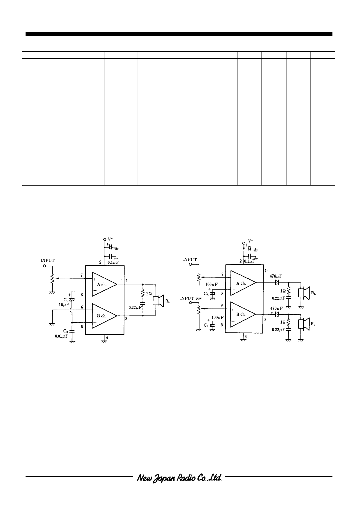
■ TYPICAL APPLICATION & TEST CIRCUIT
Fig.1 BTL Configuration Fig.2 Stereo Configuration
note:pin No.to D,M-Type
=∞ - 6 9 mA
L
THD=10%,f=1kHz
+
=6V,RL=16Ω - 240 - mW
+
=5V,RL=8Ω ( Note ) - 270 - mW
+
=4V,RL=4Ω ( Note ) 180 250 - mW
+
=3V,RL=4Ω - 120 - mW
+
=2V,RL=4Ω
THD=1%,f=1kHz
+
=4V,RL=4Ω - 180 - mW
- 30 - mW
%
=10kΩ,A Curve - 2.5 - µV
S
=10kΩ,B=22Hz~22kHz - 3 - µV
S
=-3dB from f=1kHz,RL=16Ω,PO=125mW - 200 - kHz
V
-
-
Ver.2004-03-01
Page 5
NJM2073
■ PARASTIC OSCILLATION PREVEMTING CIRCUIT
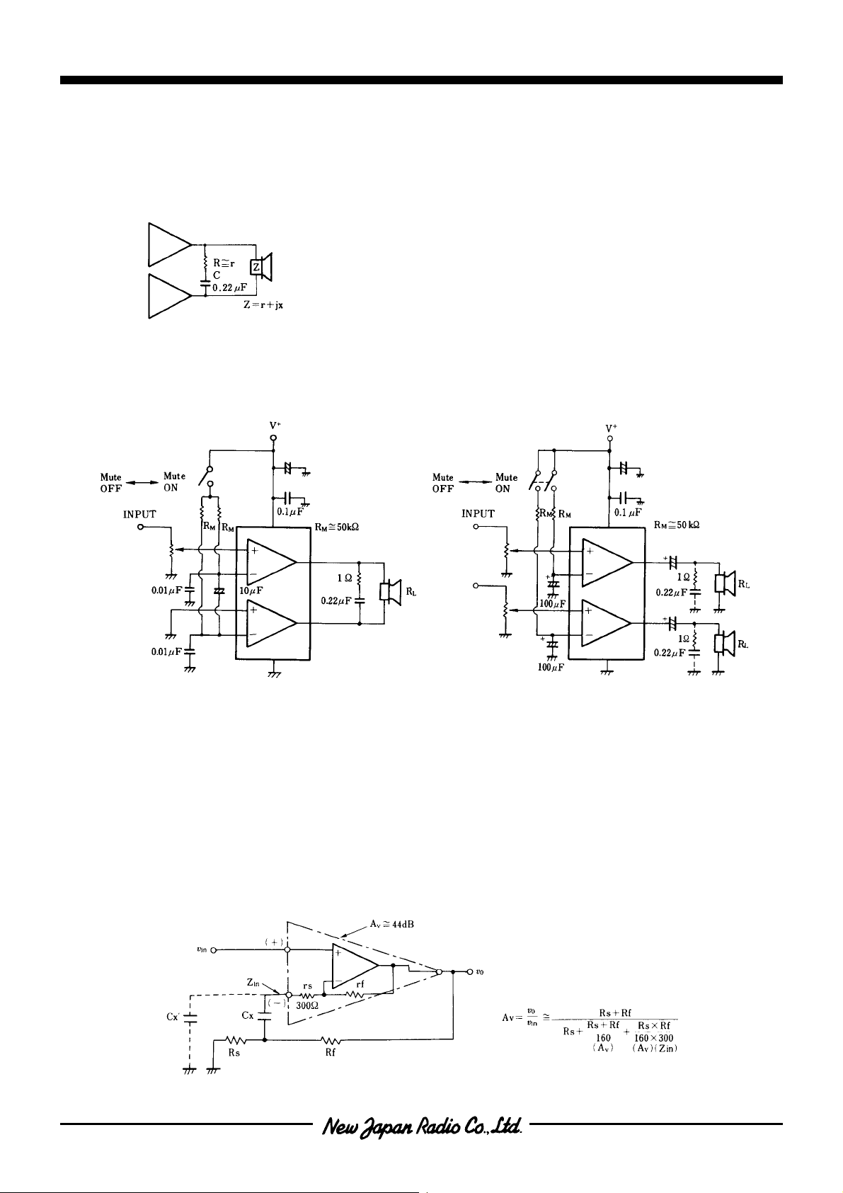
Put 1Ω+0.22µF on parallel to load,if the load is speaker.Recommend putting 0.1µF and more than 100µF capacitors with good high
frequency characteristics in to near ground and supply voltage pins.
In BTL operation of less than 2V supply voltage,parastic oscillation may be occurred with R=1Ω.And so recommended R to be the
same value of pure resistance(r) when it is lower than 3V.
■ MUTING CIRCUIT
When Mute ON.OUTPUT level saturates to GND side.
Fig.3 BTL Configuration Fig.4 Stereo Configuration
■ VOLTAGE GAIN REDUCTION APPLICATION EXAMPLE
(1) Outline of way to further Reduction
NJM2073 by taking in assamption,as one of OP-AMP ( Gain 44dB,minus input impedance about 300Ω ),to feedback from output to
minus input helps to get reduction of stabilized Voltage Gain.Fig.5 indicates the model example.
Here is the point to be noticed that,in order to get the appropriate output Bias Voltage,it is important to keep the minus input floating
as DC condition,(inserting C
phase margin.The reduction of voltage gain is limited at around 26dB (20 times),and when oscillation,it in necessary to attach the
oscillation stopper.Please examine the C
Fig.5 Model of Voltage Gain Reduction
),and also that when extended too much reduction of Gain might cause Oscillation due to high band
X
value accordingly to the application requirement.
X
Ver.2004-03-01
-
-
Page 6
NJM2073
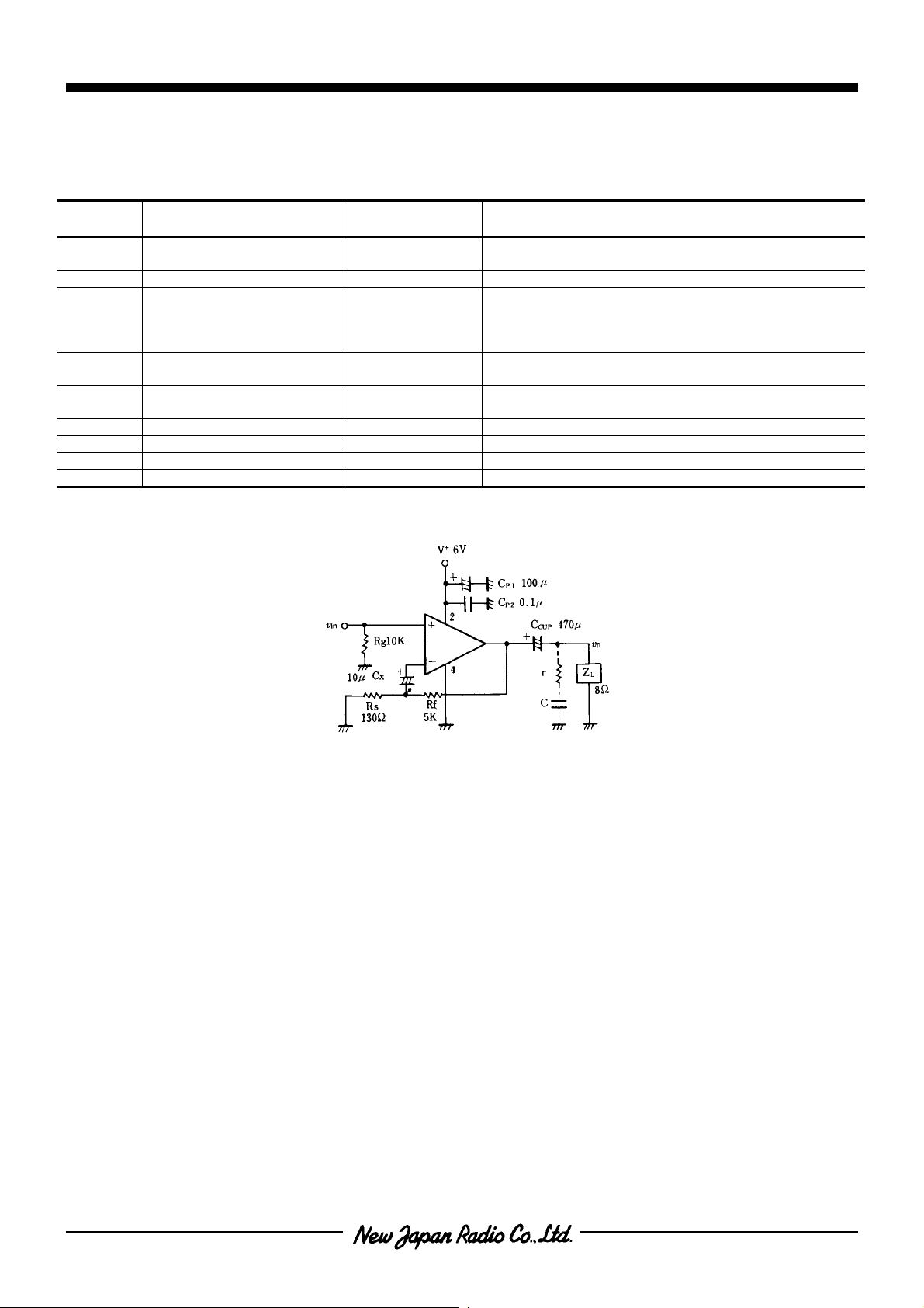
(2) The Application Example of Voltage Gain Reduction. ( STEREO )
Fig.6 indicates the application example and Table1 indicates the recommendable value of parts to be attached externally.
Table1,Applicating purpose and Recommended Value of Externally parts to be attached.
EXTERNAL
PAR TS
Rg Plus input to be grounded by
Rs AV shall be decided with Rf -
R
f
CX Minus input to be grounded by
C
Output DC Decoupling When RL=8Ω,More
CUP
CP1 Stabilization of V+ More than about C
CP2 Prevention of Oscillation More than 0.1µF
r Prevention of Oscillation About RL Inserting near around V+ pin and GND pin.
C Prevention of Oscillation 0.22µF To be examined by about the resistor volume of the speaker load.
APPLICATION PURPOSE
fixed DC
AV shall be decided with Rs About 5kΩ The co-temperature of AV becomes higher in case when RS is
fixed DC
Fig.6 STEREO Application Example.
RECOMMENDED
VAL UE
Under about 100kΩ Catch the noise when much higher.
higher resistance.The current from output pin to GND becomes
higher,in case when RS is lower resistance.(The current sinks in
vain.)
- Low-band Cut off frequency (fL) is to be decided.
The rise time becomes longer in case that C
fL shall be decided by C
than 220µF
Inserting near around V+ pin and GND pin.
CUP
REMARKS
and ZL.
CUP
is big.
X
-
-
Ver.2004-03-01
Page 7
NJM2073
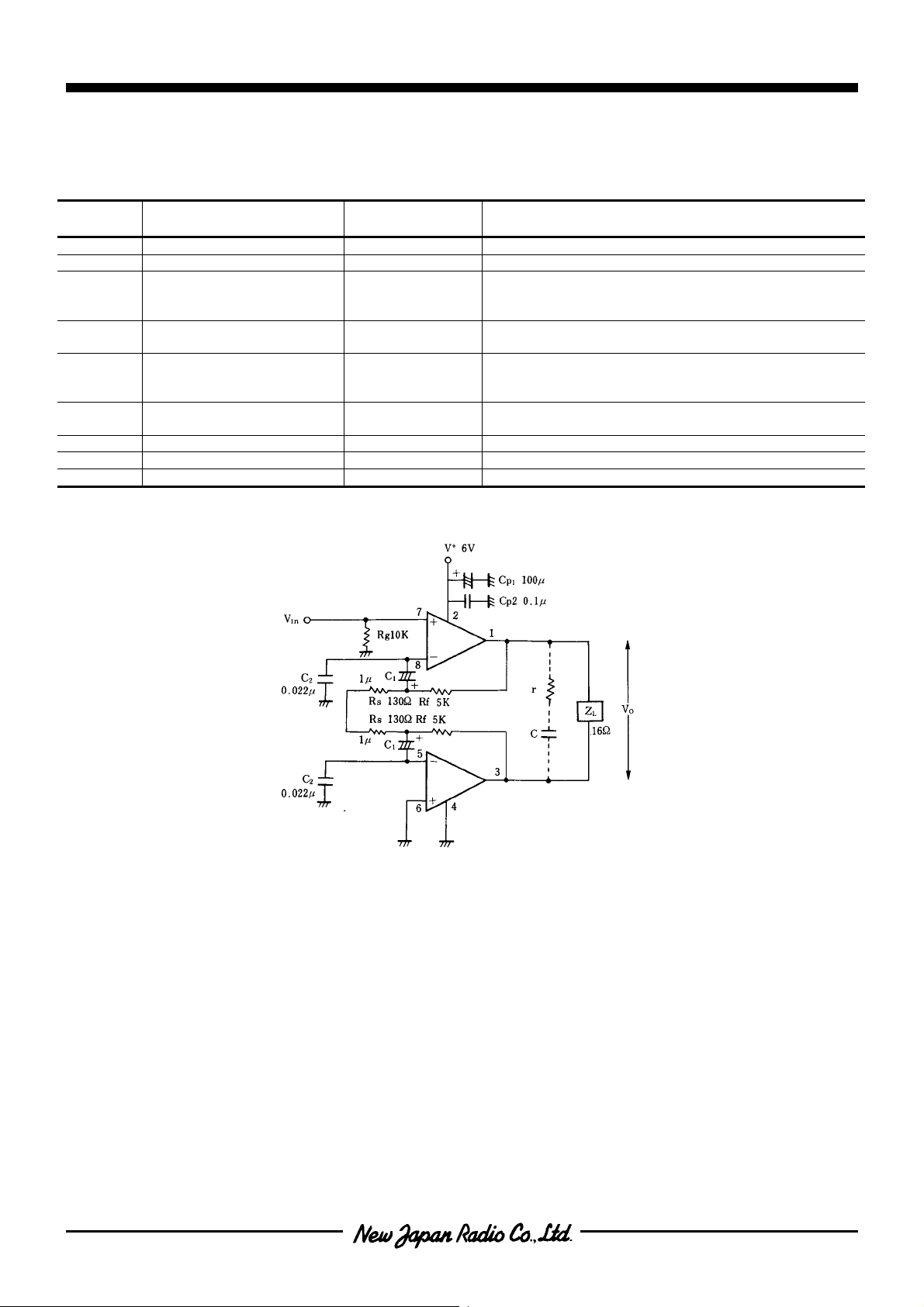
● Application for Voltage Gain Reduction ( BTL )
Fig.7 indicates the application example,Table2 shows recommended value of externally attaching parts.
Table2 Applicating purpose and Recommended Value of External Part
EXTERNAL
PAR TS
Rg DC condition ground of plus input Below about 10kΩ Making noise when higher.
Rs AV shall be decided with Rf -
R
f
C1 Releasing minus input in to DC
C2 Preventing Oscillation About 0.02µF The more higher in value,the high band THD,due to phase slipping
CP1 Stability of V
CP2 Preventing Oscillation More than 0.1µF Inserting near around at V+ and the GND pin.
r Preventing Oscillation About RL To be examined at around pure resister Value of speaker load.
C Preventing Oscillation 0.22µF
APPLICATION PURPOSE
AV shall be decided with Rs About 5kΩ Temperature feature to be increased accordingly as in higher AV
condition
+
Preventing Oscillation
Fig.7 BTL Application
RECOMMENDED
VAL UE
- Setting up low band Cut-off frequency (fL).
More than about
100µF
REMARKS
value.
When lower,to be trended of Oscillation.
More higher,the rise time become longer.
to be deteriorated.
When lower,to be trended of oscillation.
Inserting near around at V
+
and the GND pin.
Ver.2004-03-01
-
-
Page 8
NJM2073
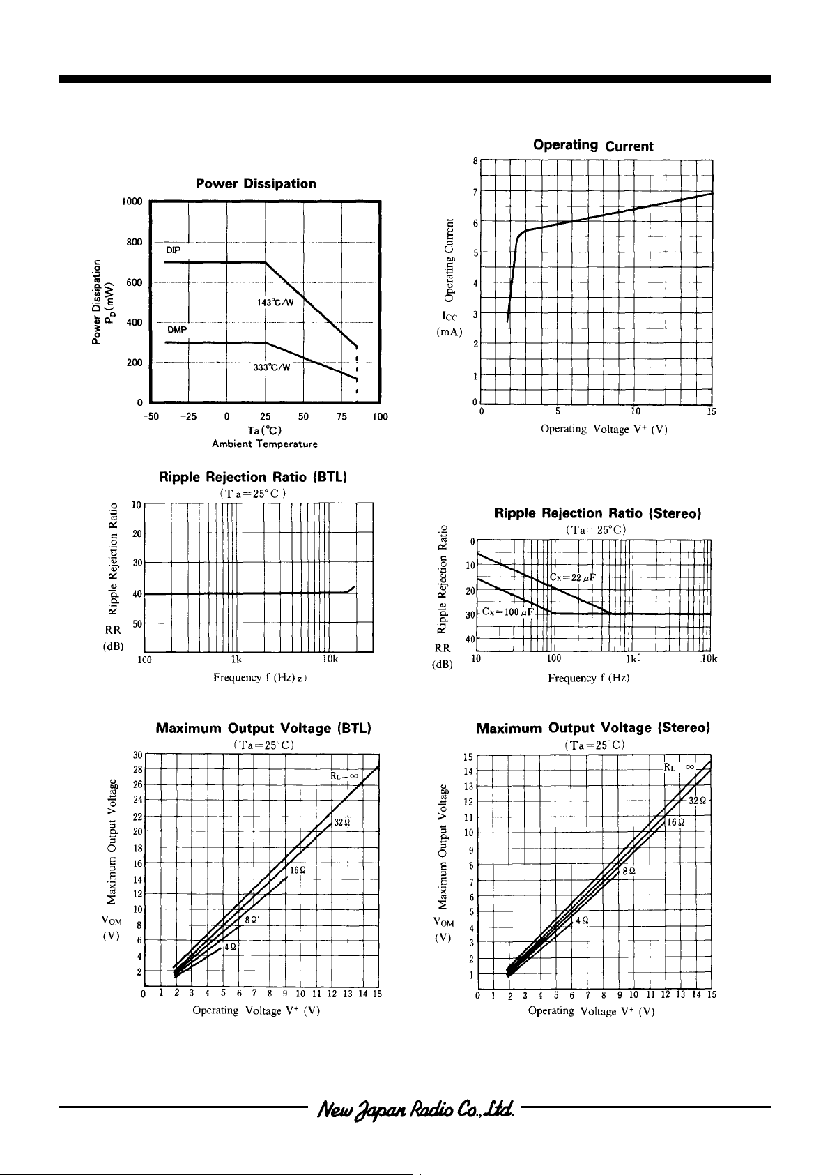
■ TYPICAL CHARACTERISTICS
-
-
Ver.2004-03-01
Page 9
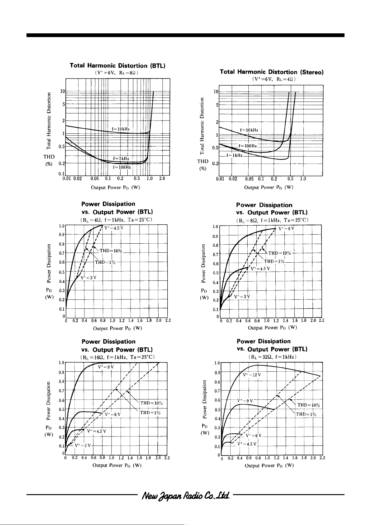
■ TYPICAL CHARACTERISTICS
NJM2073
Ver.2004-03-01
-
-
Page 10
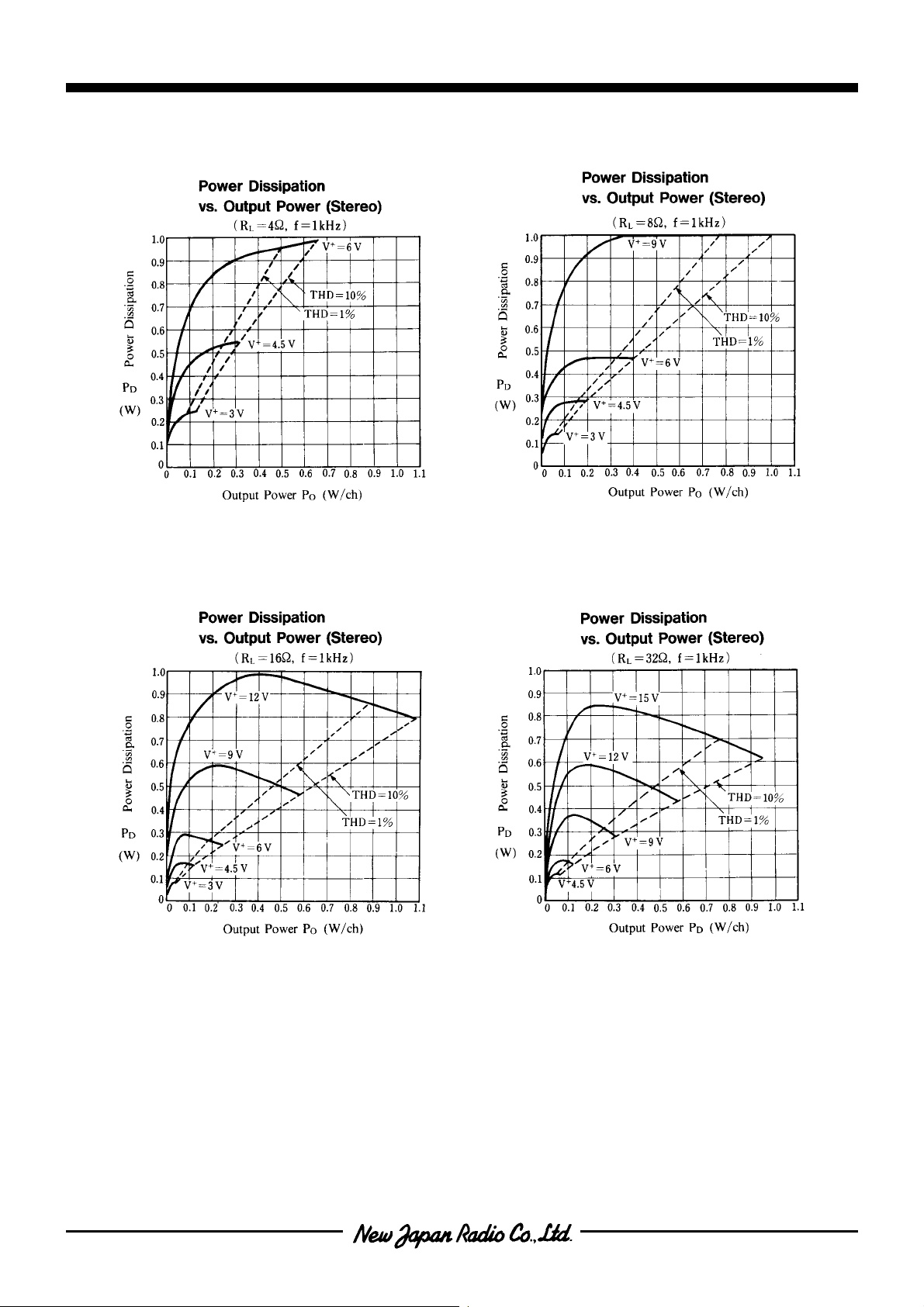
NJM2073
■ TYPICAL CHARACTERISTICS
-
-
Ver.2004-03-01
Page 11
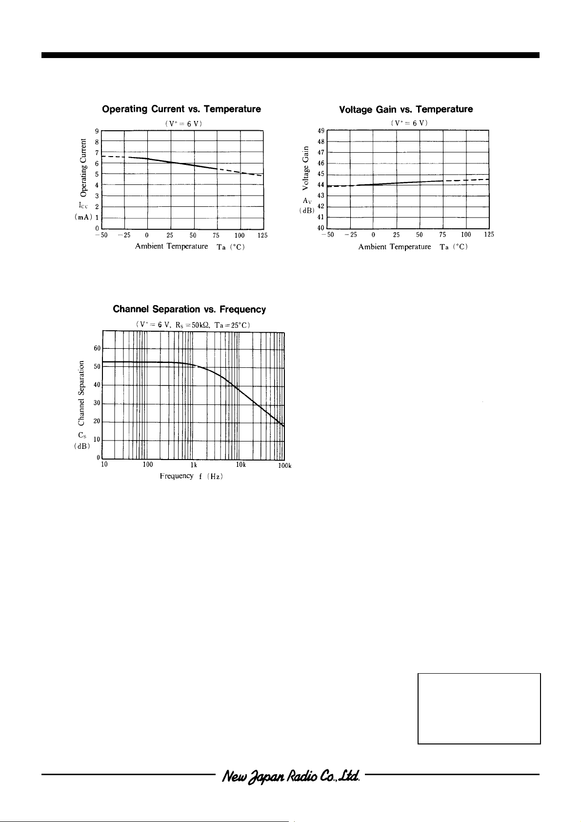
■ TYPICAL CHARACTERISTICS
NJM2073
Ver.2004-03-01
[CAUTION]
The specifications on this databook are only
given for information , without any guarantee
as regards either mistakes or omissions. The
application circuits in this databook are
described only to show representative usages
of the product and not intended for the
guarantee or permission of any right including
the industrial rights.
-
-
 Loading...