

Page 1

THIS DOCUMENT IS FOR MAINTENANCE
PURPOSES ONLY AND IS NOT
RECOMMENDED FOR NEW DESIGNS
Page 2
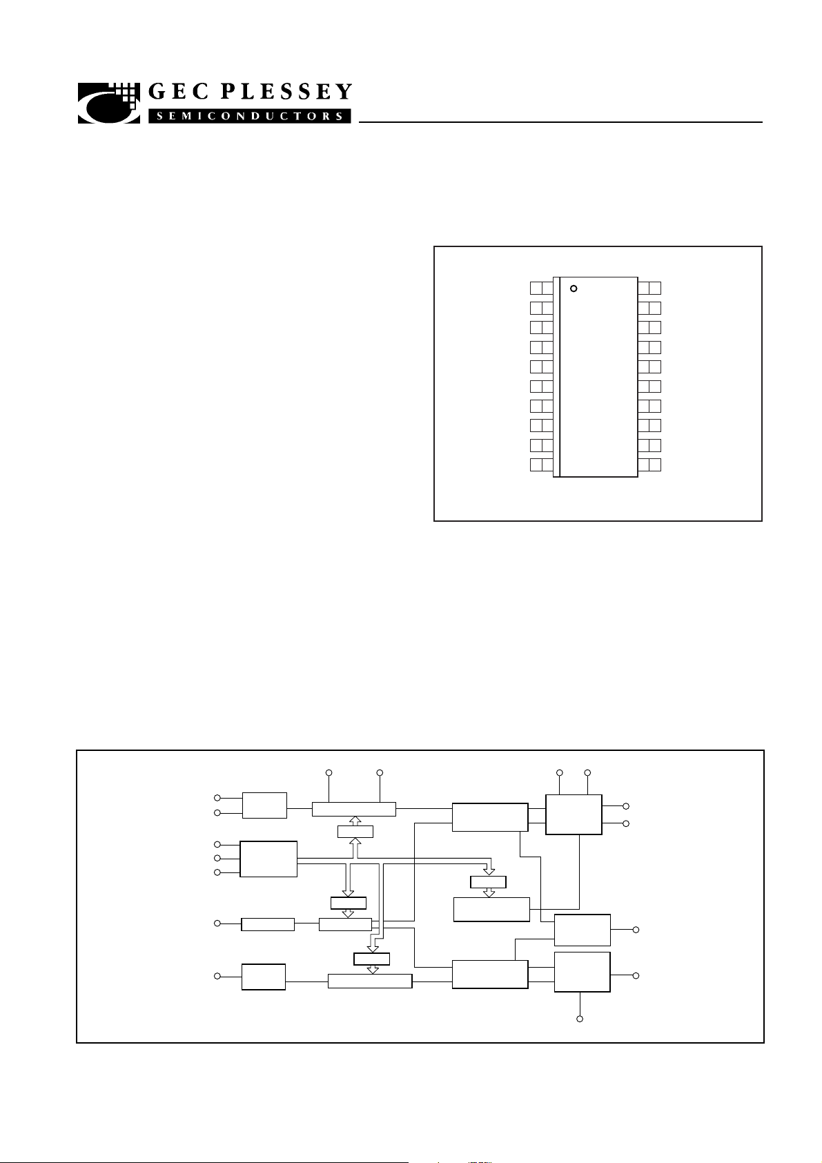
NJ88C51
DUAL LOW POWER FREQUENCY SYNTHESISER
The NJ88C51 is a low power integrated circuit, designed
as the heart of a fast locking PLL subsystem in a mobile radio
application. It is manufactured on GEC Plessey
Semiconductors 1.4 micron double polysilicon CMOS
process, which ensures that low power and low noise
performance is achieved. The device contains two
synthesisers, one for the generation of VHF signals up to
125MHz and a second for UHF (when used with a
mulitmodulus prescaler such as the SP8713/14/15). The
main synthesiser has the capability of driving a dual speed
loop filter and also can perform Fractional-N interpolation.
Both synthesisers use current source outputs from their
phase detectors to minimise external components. Various
sections may be powered down for battery economy.
FEATURES
■ 30MHz main synthesiser
■ 125MHz auxiliary synthesiser
■ Programmable output current
from phase detector - up to 10mA
■ High input sensitivity
■ Fractional-N interpolator
■ Supports up to 4 modulus prescalers
■ SSOP package
■ Lock Detect Output
■ Low noise modulus control outputs
APPLICATIONS
■ NMT, AMPS, ETACS cellular
■ GSM, IS-54, RCR-27 cellular
■ DCS1800 microcellular
■ DLMR, DSRR, TETRA
■ DECT, PHP cordless telephones
MAY 1994
DRAFT SPECIFICATION
DS3907 - 1.4
DATA
STROBE
FIM
FIMB
AGND
RI
AVDD
FIA
RSA
PDA
1
2
3
4
NJ88C51
5
6
7
8
9
10 11
NP20
Fig.1 Pin assignment
ABSOLUTE MAXIMUM RATINGS
Storage temperature -55°C to +150°C
Operating temperature -40°C to +85°C
Supply voltage -0.5 to 7.0V
Voltage on any pin -0.3V to (VDD + 0.3V)
ORDERING INFORMATION
NJ88C51\IG\NPAS - (Industrial temp range in SSOP
package)
20
CKIN
19
MOD2
18
MOD1
17
LD
16
RSC
15
RSM
14
VDD
13
PDP
12
GND
PDI
FIM
FIMB
DATA
CKIN
STROBE
FIA
MOD2MOD1
MAIN N
BUFFER
SERIAL
INPUT
REGISTER
RI
R BUFFER
AUX. N
BUFFER
MAIN N-DIVIDER
LATCH
LATCH
R DIVIDER
LATCH
AUX. N-DIVIDER
QBAR
Q
PHASE
DETECTOR
LATCH
FRACTIONAL-N
SYSTEM
PHASE
DETECTOR
RSMRSC
CURRENT
SOURCE
LOCK
DETECT
CURRENT
SOURCE
RSA
PDI
PDP
LD
PDA
Fig.2 Simplified block diagram
Page 3

NJ88C51
PIN DESCRIPTION
Pin
Name
1
DATA
2
STROBE
3
FIM
4
FIMB
5
AGND
6
RI
7
AVDD
8
FIA
9
RSA
10
PDA
11
PDI
12
GND
13
PDP
14
VDD
15
RSM
16
RSC
17
LD
18
MOD1
19
MOD2
20
CKIN
It is recommended that power supply pins are well decoupled to minimise power rail born interference.
Function
Serial input for programming data.
Program enable pin, active low.
Main synthesiser balanced input buffer, may be used with single ended prescaler output if Fimb
is biased.
Main synthesiser balanced input buffer, may be used with balanced prescaler output, or biased
for single ended operation.
Analogue ground supply pin.
Master reference frequency input, should be a.c coupled from an accurate source.
Analogue supply pin (nominally 5V).
Auxiliary synthesiser frequency input, should be a.c coupled.
Current setting resistor connection defining auxiliary phase detector output current.
Tristate current output from auxiliary phase detector.
Tristate current output from the main synthesiser's phase detector giving integral control.
Digital ground supply pin.
Tristate current output from the main synthesiser's phase detector giving proportional control.
Digital supply pin (nominally 5V).
Current setting resistor connection defining main synthesiser's phase detector output currents.
Current setting resistor connection defining the compensation current for fractional-N ripple
elimination in the main synthesiser's current source outputs.
Lock Detect Output
Modulus control pin (see truth table).
Modulus control pin (see truth table).
Serial clock input for programming bus.
ARCHITECTURE
Fig.2 shows a simplified block diagram of the NJ88C51, a
more detailed description of each block and its function is
given later in this datasheet.
The synthesiser consists of the following blocks
- 35MHz reference frequency input buffer
- 35MHz programmable reference divider
- 125MHz Auxiliary synthesiser input buffer
- 125MHz Auxiliary synthesiser programmable divider
- Auxiliary synthesiser phase detector with current source
outputs
- 30MHz main synthesiser input buffer (differential inputs)
- 30MHz main synthesiser programmable divider and control
logic
- Main synthesiser Fractional-N interpolation system
- Main synthesiser phase detector with dual current source
outputs
2
Page 4
NJ88C51
DQ
R
DQ
R
Variable
N-Divider
Pulse
Reference
Divider
Pulse
Enable pull-down
charge pump
Enable pull-up
charge pump
+
+
FUNCTIONAL DESCRIPTION
The NJ88C51 has been designed using a modular
concept, and its operation can be best summarised as these
component blocks.
Reference divider
The reference divider is used to provide the reference
signals needed for both the main and auxiliary synthesiser
phase detectors. The divider allows for a twelve bit number to
be loaded, via the serial bus, to select the required division
ratio. Division ratios of 3 to 4095 can be used.
The reference divider input stage will accept a low level,
AC coupled, sinewave input. It is anticipated that in most
systems this will be provided by a stable reference source up
to 35MHz, and so encompasses all the common TCXO
(temperature controlled crystal oscillator) frequencies, such
as 9.6, 12.8, 13.0, 19.44 and 26MHz.
A standby mode is supported so that the reference divider
can be powered down, this is achieved using two of the serial
program control bits.
To reduce the possibility of unwanted interaction between
the main and auxiliary synthesisers, the charge pumps do not
take current at the same time. To achieve this the output of the
reference divider has a duty factor of approximately 50:50,
which then allows the Q and QBAR taps to be used for the
auxiliary and main synthesisers respectively. By doing this the
current pulses can be taken alternatively, minimising
modulation of the power supply rails as current is drawn.
The reference divider consists of a 12 bit programmable
divider followed by a 4 bit binary counter. This 4 bit counter
gives a choice of divide by M, 2M, 4M or 8M.
A pair of programmable control bits are used to determine
which of the divide by M, 2M, 4M or 8M outputs is supplied to
the auxiliary synthesiser’s phase detector and a further pair of
control bits are used to determine which are supplied to the
main synthesiser’s phase detector.
The charge pump output current level is set by an external
resistor on the RSA pin (pin 9) up to a limit of 250µA +/-10%.
A pull up current pulse will indicate that the VCO frequency
must be increased, whilst a pull down pulse indicates that the
frequency must be decreased.
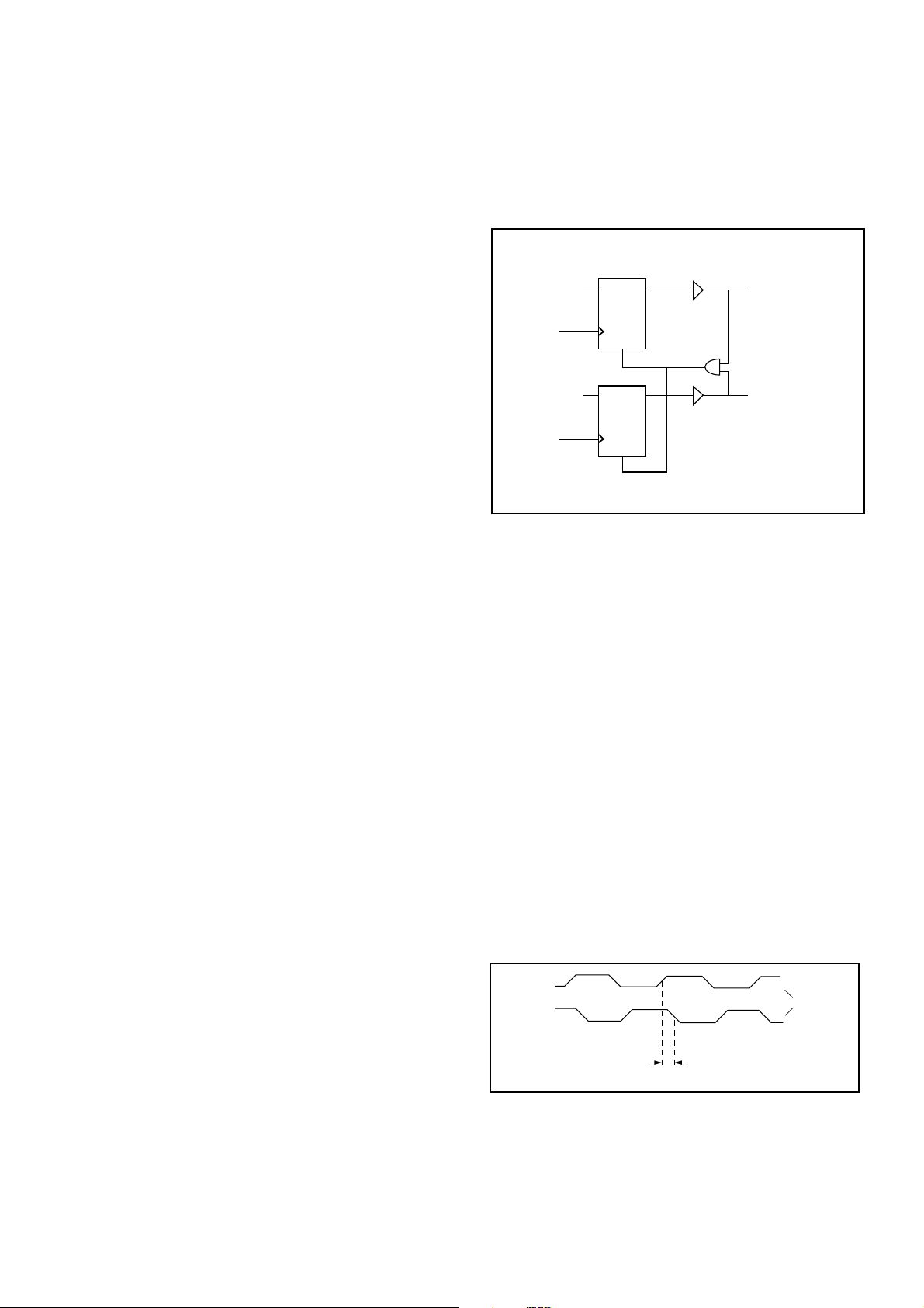
Fig.3 Auxiliary phase detector
Main Synthesiser
The main synthesiser is capable of operating at
frequencies up to 30MHz. The synthesiser uses the 12 bit
reference divider, shared with the auxiliary synthesiser, a 12
bit up/down N divider and a digital phase comparator with
current source outputs.
The device also has a number of features which increase
the design flexibility and performance of the synthesiser.
These include fractional-N operation, speed up mode and
support of 2, 3 and 4 modulus prescalers. A description of the
operation and advantages of each of these features is given.
Auxiliary synthesiser
The auxiliary synthesiser operates over an input frequency
range from 1 to 125MHz, without the use of an external
prescaler. The synthesiser consists of a 12 bit N divider and
a digital phase comparator with current source outputs. The
reference frequency is supplied by the shared reference
divider. Current source outputs allow a passive loop filter to
be used.
When the auxiliary synthesiser is not in use, a standby
mode is supported so that power consumption is reduced.
This is achieved using one of the serial program control bits.
The divider is programmed with a 12 bit word allowing
division ratios of 3 to 4095 to be used.
The auxiliary phase detector consists of the 2 D-type
phase and frequency detector shown in Figure.3 below, the
high and low outputs of which drive on-chip, opposing
complementary charge pumps. This type of phase detector
design eliminates non linearity or deadband around the zero
phase error (locked) condition.
The main N divider input buffer will accept inputs from
an external prescaler, either as balanced (2 wire) ECL levels
at frequencies up to 30MHz, or DC coupled to a single ended
prescaler output. Single ended operation requires the other
buffer input (pin 3) to be externally biased to the correct slicing
voltage for the prescaler and also externally decoupled.
If the inputs are in the form of balanced ECL levels, there
must not be a skew of greater than 2ns between one input
changing and the second input changing. The relationship of
the signals is shown below in Fig.4.
FIM
FIMB
+/-2ns
Fig.4 Maximum input skew
Balanced
E.C.L
Inputs
3
Page 5
NJ88C51
The main N divider is programmable so that it can
determine how many cycles of each division ratio the external
prescaler will perform.
The total division ratio of the output from the system VCO
to the synthesiser's phase detector may be expressed as NTOT
and R1, R2, R3 and R4 are the available prescaler ratios and
N1, N2, N3 and N4 are the corresponding number of cycles for
each ratio selected, within one complete division cycle.
The divider is programmed via the serial data bus and the
values needed to be programmed for each of the possible
prescaler ratios are as follows:-
In 2 modulus mode (division ratios R1, R2)
NTOT = N1.R1 + N2.R2
Programmed values needed:
N1 - a 12 bit value giving the number of times R1 is to be used
N2 - a 8 bit value giving the number of times R2 is to be used
In 3 modulus mode (division ratios R1, R2, R3)
NTOT = N1.R1 + N2.R2 + N3.R3
Programmed values needed:
N1 - a 12 bit value giving the number of times R1 is to be used
N2 - a 4 bit value giving the number of times R2 is to be used
N2+N3 - a 4 bit value where N3 is the number of times R3 is
to be used and (N2+N3) is modulo-16 addition
In 4 modulus mode (division ratios R1, R2, R3, R4)
NTOT = N1.R1 + N2.R2 + N3.R3 + N4.R4
Programmed values needed:
N1 - a 12 bit value giving the number of times R1 is to be used
N2 - a 4 bit value giving the number of times R2 is to be used
N2+N3 - a 4 bit value where N3 is the number of times R3 is
to be used.
N2+N3+N4 - a 4 bit value where N4 is the number of times R4
is to be used. (N2+N3) and (N2+N3+N4) are modulo-16
addition.
To facilitate the use of multimodulus prescalers the N
divider is based upon a twelve bit up/down counter which
functions as follows
The first value, N1, is loaded into the counter which then
counts down from N1 to zero. During this time, the modulus
ratio R1 is selected.
When the counter reaches zero modulus R2 is selected
and the counter then counts up to the N2 value. If 2 modulus
operation is chosen, the counter is then reloaded with N1 and
the count is repeated.
For operation with 3 or 4 modulus devices, the counter
continues to count up once it has reached the N2 value. The
count continues to the N2+N3 value and during this time the
R3 ratio is selected. In the 3 modulus case, when the N2+N3
value is reached the counter is then reloaded with the N1
value and the modulus ratio R1 is selected.
For 4 modulus operation the counter will continue its count
up to the N2+N3+N4 value before reloading the N1 value.
During this time the R4 modulus is selected.
If N2, N3, or N4 are set to zero this will give a full count of 16
for the corresponding modulus.
The N divider block also has a special control line from the
Fractional-N logic. When required this control will cause the
total division ratio to be increased from N to N+1. This is
achieved by forcing a cycle which would have normally used
a prescaler ratio R1 to use ratio R2 instead. R1 and R2 are
chosen so that R2 equals R1+1.
Further explanation of the operation of the synthesiser
when using 2, 3 or 4 modulus prescaler is given in the section
on multimodulus division (page 8).
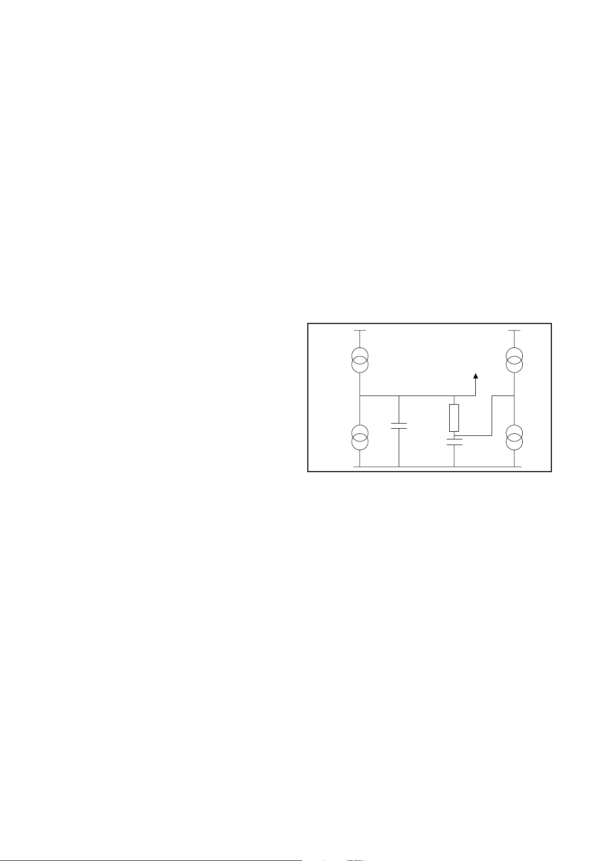
The phase detector used on the main synthesiser is
similar to the type used on the auxiliary synthesiser (Figure.3).
In this case, however, the detector will drive two pairs of
complimentary charge pumps, one of which is intended to
drive the loop integrator capacitor to provide integral control,
whilst the other provides proportional control for the VCO.
This system is shown in Fig 5, and has applications where fast
locking of the loop is required.
Vdd Vdd
TO VCO
PROPORTIONAL
CHARGE
PUMP
Fig.5 Loop filter using both charge pumps
INTEGRAL
CHARGE
PUMP
Gnd
MODES OF OPERATION
Normal Mode
The synthesiser will operate in normal mode while the
strobe line of the serial data bus is low. In this mode the
following current levels are produced. The charge pump
providing the proportional feedback term will have a normal
current level designated by Iprop(0), that is set by an external
bias resistor, RSM. Iprop(0) will vary when different N-divider
ratios are programmed, so that it is proportional to the total
division ratio. To avoid the necessity of computing the total
division ratio on chip, an eight bit number representing the
most significant bits of Ntot will be loaded via the serial data
bus. Iprop(0) is therefore given by
Iprop(0) = CN.Ibo
where CN is the loaded eight bit number and the value Ibo is
scaled from the external current setting resistor RSM where
Ibo = Irsm/32. Typically Ibo = 1µA ,and therefore Iprop(0) will
have a maximum value equal to 255µA.
4
Page 6

NJ88C51
The normal value of Iprop, Iprop(0), is obtained while the
strobe line of the serial programming bus is held low. In this
condition, the second charge pump providing the integral
feedback term is inactive.
Speed up Mode
In speed up mode the loop bandwith during switching
is increased to allow faster initial frequency acquisition. This
is done by using the dual phase detector outputs (PDP and
PDI) connected to a standard passive loop filter as shown in
fig.5. The effect of this is to increase the loop gain and hence
the bandwidth while maintaining a constant phase margin
when switching between speed up mode and normal mode.
The synthesiser operates in speed up mode when the
strobe line goes high loading either word A or word A2 (see
programming section Page 8-Page 9) and it will stay in this
mode until the strobe line goes low. In this mode the following
current levels are produced. The charge pump providing the
proportional feedback will increase its current from Iprop(0) to
a value Iprop(1), where
L+1
Iprop(1) = 2
.Iprop(0)
where L is a two bit number loaded as part of the serial
programming data. Iprop(1) will therefore be 2, 4, 8 or 16
times Iprop(0). The charge pump supplying Iprop is specified
up to a value of 1mA.
Also when the strobe line goes high loading word A or
word A2, the charge pump providing the integral feedback
term becomes active at a current level Iint given by
Iint = K.Iprop(1)
ratio. Using fractional-N the value of N is alternated between
N and N+1 in order to simulate a fractional part. For example
9000.375 would be simulated by alternating between 9000
and 9001 in the pattern
9000, 9000, 9001, 9000, 9000, 9001, 9000, 9001 (mean value of 9000.375).
On the NJ88C51 the fractional-N circuit consists of an
accumulator which can be set to overflow at a value of 5 or 8
(FMOD in programming word D, see page 9). The value in the
accumulator, A, is incremented once every comparison cycle
of the main phase detector and every time the accumulator
overflows the total division ratio of the synthesiser and
prescaler is increased from N to N+1. To obtain the pattern
described above N=9000 and FMOD would be set to mod8
and the incremental value, NF(programmed in word A) would
be set to 3. The accumulator would then behave as shown
below.
Increment Accumulator Total Division
Value Value Ratio
3 3 9000
3 6 9000
3 1 9001
3 4 9000
3 7 9000
3 2 9001
3 5 9000
3 0 9001
Varying NF allows different fractions to be obtained. If NF=1
and FMOD=8 the accumulator would overflow once in every
8 cycles giving a value of 9000.125. Similarly if NF=4 the
accumulator overflows every other cycle giving 9000.5.
where K is a four bit number loaded as part of the serial
programming data. Although Iint can be programmed to be
240 times greater than Iprop(0), the charge pump supplying
Iint is only specified up to a value of 10mA.
For all charge pumps, a pull-up current indicates the VCO
frequency should be increased while a pull-down current
indicates the VCO frequency should be decreased.
For the proportional and integral charge pumps, the
selected pulse current levels will remain substantially
constant over the charge pumps, output voltage ranges
tabulated in the electric characteristics. “Substantially
constant” means that the current will not have changed by
more than 10% of the value measured at 2.5 volts on the
output .
FRACTIONAL-N OPERATION
Conventional, non fractional-N synthesisers have a
frequency resolution or step size equal to the phase detector
comparison frequency. Fractional-N refers to a technique
which allows finer frequency steps to be obtained.
The synthesised frequency with a conventional
synthesiser is equal to N times the phase detector comparison
frequency, where N is the programmable integer loop divide
For a given step size this increase in resolution means a higher
comparison frequency at the phase detector, and therefore a
lower overall division ratio. For example,
with a step size = 200kHz
and carrier frequency = 900MHz
Non fractional-N synthesiser
Comparison frequency=200kHz
Division ratio=900MHz=4500
200kHz
Fractional-N synthesiser (using 5ths)
Comparison frequency=1MHz
Division ratio=900MHz=900
1MHz
In most applications the phase noise is proportional to the
overall division ratio. Therefore fractional-N gives lower phase
noise. This higher comparison frequency and lower phase
noise allows circuits to be built with wider loop bandwidths
while keeping the same stability. This means that phase
locked loops (PLLs) can be made to either switch faster for a
given phase noise or be quieter for a given switching speed,
compared to conventional designs.
5
Page 7

NJ88C51
However the alternation between the N and N+1 values
causes a ripple in the output frequency. This ripple is not
desirable in radio frequency synthesisers. This ripple or jitter
waveform is predictable from the pattern of N and N+1 values
and so can be cancelled.
The instantaneous accumulator value, A, is proportional to
the cumulative frequency error caused by ignoring the
fractional part during the periods of the divide by N. The
accumulator value, A, may therefore be used to generate a
waveform corresponding to the jitter waveform, that is then
used to cancel the jitter out of the phase detector. This jitter
compensation current pulse is equal to A.Icomp where Icomp
represents the step size as A is incremented.
Corresponding to the two alternative values of Iprop,
Iprop(0) and Iprop(1), Icomp will take the values Icomp(0) and
Icomp(1). Icomp is always pull-up, and the magnitude of its
steps for perfect jitter compensation are related to the value
of Iprop by the factors
0 , 1/Q.Ntot , 2/Q.Ntot , 3/Q.Ntot ........ Q-1/Q.Ntot
where Q = accumulator modulus in use (5 or 8)
Since
Iprop(0) = CN.Ibo
and CN is an approximation to Ntot apart from a scaling factor,
the value of Icomp(0) required becomes independent of Ntot
and its steps are
0 , 1/Q , 2/Q , 3/Q ........ Q-1/Q times Ibo.(scaling factor)
where scaling factor = Max. value of CN to be used
Corresponding max. value of Ntot
therefore Ico = 1 x CN(max) x Ibo
Q Ntot(max)
and Icomp(0) = A.Ico
where Ico is scaled from the external current setting resistor
RSC.
Ico = Irsc/128.
Typically Ntot(max) might be 10000, with CN(max)=250
and Q=8, so the current step will be of magnitude Ibo/320.
Since Ibo is only 1 uA, this is a very small value; however this
value only applies if Icomp is a continuous current. Icomp
however will be a short current pulse coincident with the Iprop
pulse, in order to cancel jitter components over the widest
possible frequency range.
When the duty factor of Icomp is taken into account, its pulse
value may be increased accordingly. Icomp is therefore
generated as a pulse of fixed width equal to two periods of the
input reference clock frequency, with a timing that straddles
the active edge of the reference divider output pulse supplied
to the main phase detector, as shown below: (Fig 6).
Since the duty factor of Icomp is 2/M and depends on the
value of M programmed, it is possible to set the peak pulse
value of Icomp(0) by means of the external current setting
resistor RSC to correspond with the value of M intended, the
value of ‘scaling factor’ defined above, the accumulator
modulus Q and the value of Ibo set by the other current setting
resistor.
therefore Ico = 1 x Nmax x M x Ibo
Q Ntot(max) 2
This gives a typical value for Ico of 0.1µA.
The two values of Icomp, Icomp(0) and Icomp(1) are related
by
Icomp(1) = 2
L+1
.Icomp(0)
Icomp(0) occuring when the strobe line is low and Icomp(1)
occuring when the strobe line is high loading either WORDA
or WORDA2 (see programming section, page 8 and 9) .
Corresponding to the pull-up pulse Icomp(1) that is added
to the proportional charge pump pulse Iprop(1), there is also
a pull-up current pulse Icomp2 which is added to the integral
charge pump pulse Iint. This pulse Icomp2 only applies when
the stobe line is high (loading either WORDA or WORDA2).
When the strobe line is low there will be no Iint or Icomp2
pulses. The value of Icomp2 is given by
Icomp2 = Icomp(1).K
where K is a four bit number entered as part of the serial
programming data.
M cycles of the reference input frequency
Active edge
Reference to phase detector
Timing of Icomp pulse
2 reference frequency cycles
6
Fig.6
Page 8
NJ88C51
MULTIMODULUS DIVISION
The NJ88C51 has two modulus control outputs (MOD1,
MOD2) allowing its use with 2,3 and 4 modulus prescalers.
The outputs have a reduced voltage swing to minimise
switching noise whilst maintaining compatability with GPS
prescalers. Two modulus prescalers such as the SP8714/15
are commonly used in PLLs. Additional information on using
2 modulus prescalers can be found in application note AN132
in the GEC Plessey Semiconductors Personal
Communications handbook (May 1992).
When using a 2 modulus prescaler (R/R+1) the minimum
division ratio above which all channels can be synthesised is
given by
Minimum division ratio = R(R-1)
eg. for a 64/65 prescaler such as the SP8714/15
Minimum division ratio = 64(64-1) = 4032
When fractional-N operation is being used higher comparison
frequencies are used, which are obtained by using lower
division ratios. Use of a 3 or 4 modulus prescaler allows the
minimum division ratio to be lowered.
For a 3 modulus prescaler (R/R+1/R+A)
Minimum division ratio = R(R+A+1)+A
A
eg. for a 64/65/72 prescaler such as the SP8713
Minimum division ratio = 64(64+8+1)+8 = 1096
8
For a 4 modulus prescaler (R/R+1/R+A/R+B)
Minimum division ratio = R(A+B+R+1)+A+B
A B
eg. for a 64/65/68/80 prescaler
If a 64/65 prescaler is used not all the channels will be
selectable as the minimum required division ratio is less than
the minimum allowable division ratio (4032).
If a 64/65/72 prescaler is used all the channels will now be
selectable as the minimum required division ratio will now be
greater than the minimum allowable division ratio (1096).
Modulus output truth table
MOD2
0
0
1
1
MOD1
1
0
0
1
Prescaler modulus
R1
R2
R3
R4
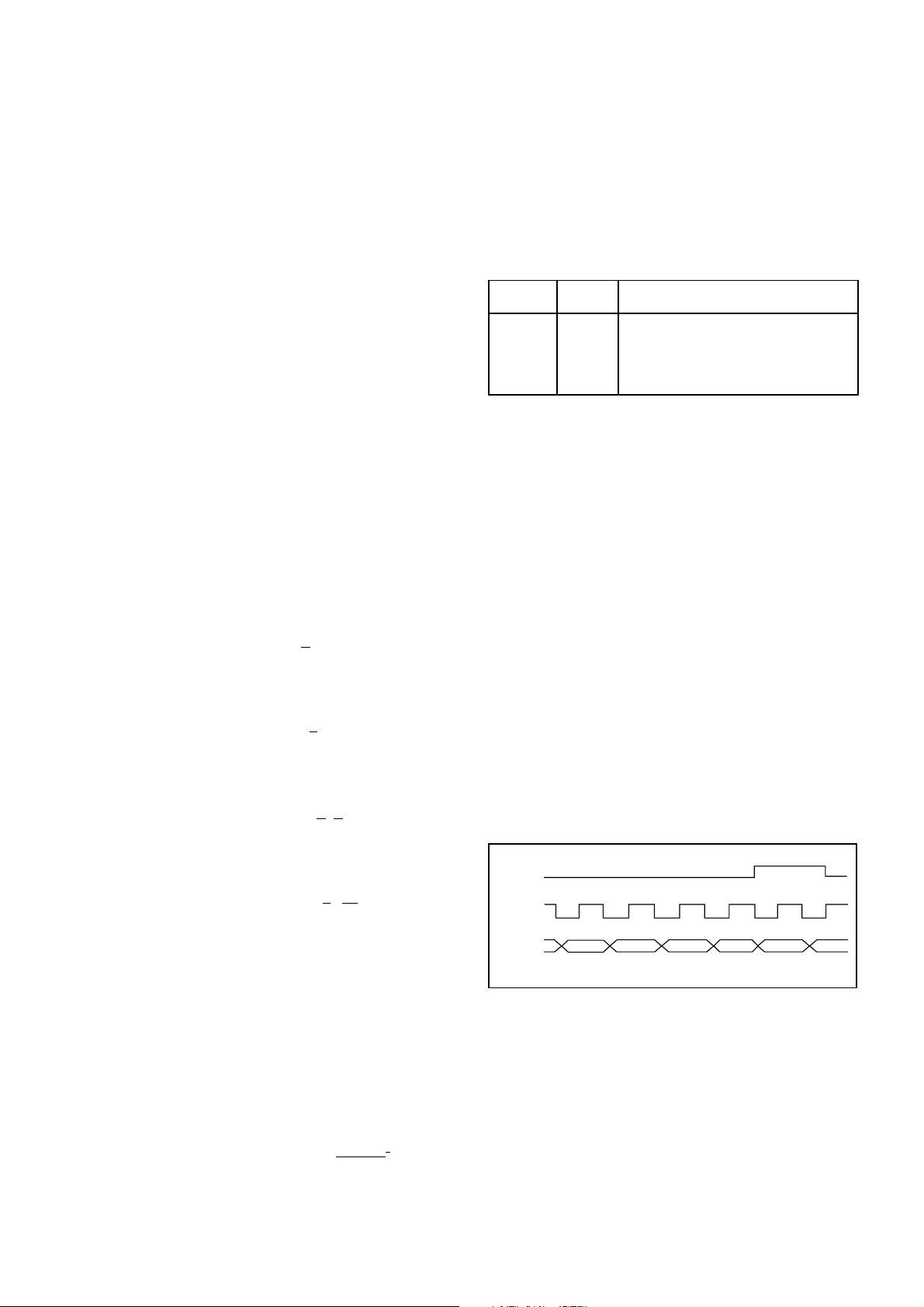
SERIAL DATA BUS
The data needed to program the synthesiser is entered via
a high speed (10MBit/s) 3-wire bus, with serial data, serial
clock and strobe pins. The input data is partitioned so that
after initial programming the output frequency can be
changed by re-programming only 24 or 32 bits.The timing
diagram for the bus is given in Fig.7.
The data is programmed as either four twenty-four bit
words or three twenty-four bit words and one thirty-two bit
word. When initially programmed words A, B, C and D are
loaded, though if the auxiliary synthesiser is disabled C is not
needed. Following the initial programming the frequency can
be subsequently shifted in one of the following ways:
a) If a 2 or 3 ratio prescaler is being used and CN does
not need to be reprogrammed word A should be
loaded.
b If a 2 or 3 ratio prescaler is being used and CN does
need to be reprogrammed word A2 should be loaded.
In wide frequency band systems CN must be
reprogrammed for best performance every time the
frequency is changed.
c) If a four ratio prescaler is being used word A and word
B should be loaded
Minimum division ratio = 64(4+16+64+1)+4+16 = 852
4 16
An example of where three modulus division would be
implemented is given below.
The system in which the synthesiser is to operate has a lowest
carrier frequency of 900MHz and a channel spacing of 30kHz.
However due to the lock up time requirements fractional-N
operation is being used in its 8ths mode (see section on
fractional-N operation), giving a comparison frequency of
30kHz x 8 = 240kHz.
Therefore,
Minimum division ratio required = 900x10
240x10
6
= 3750
3
STROBE
CKIN
DATA MSB
Data must be valid on positive edges of clock
Fig.7
A strobe pulse occurs at the end of each word and loads
the contents of the input shift register into the working
registers, except when word B is being loaded, in which case
the shift register contents are loaded into a temporary register
and then loaded into the working register when either word A
or A2 is loaded. The information is transferred on the rising
edge of the strobe pulse which should occur one half clock
period after the clock edge on which the MSB of a word is
shifted in.
7
Page 9
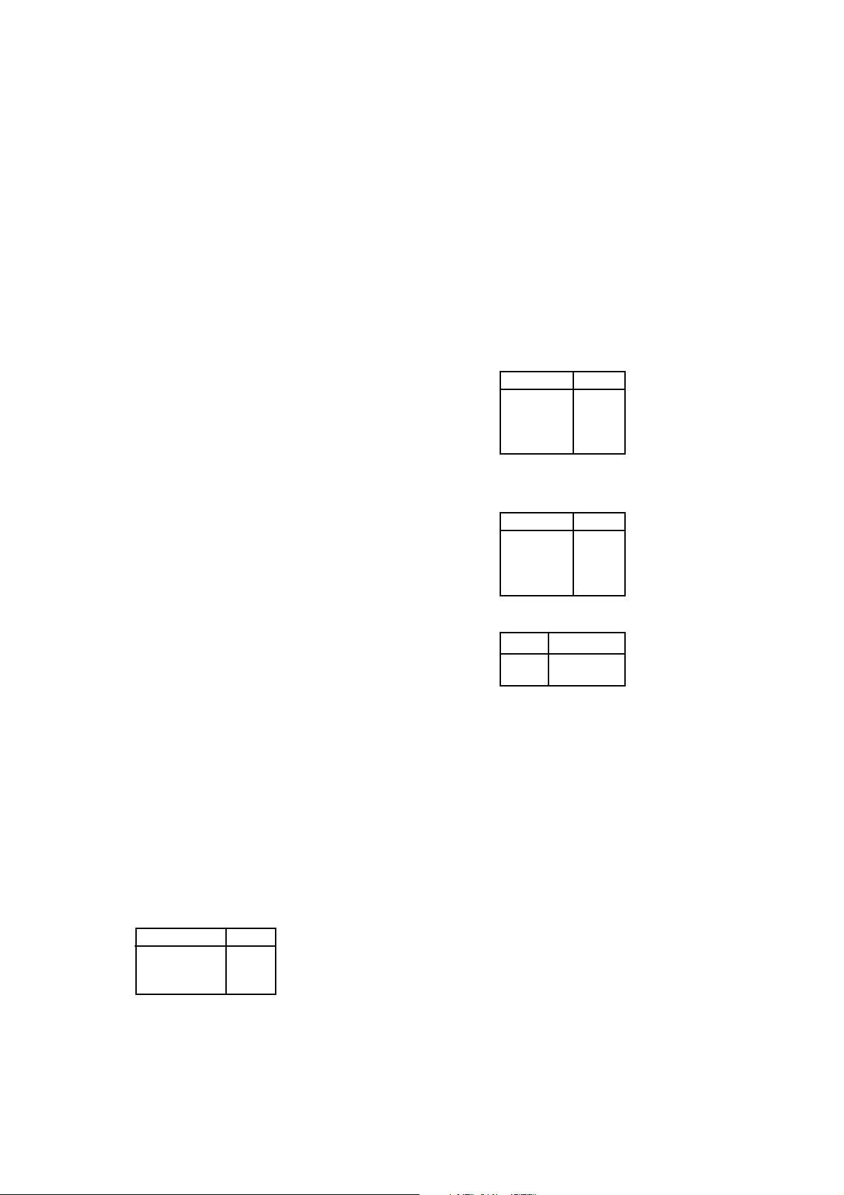
NJ88C51
If word A or word A2 is being loaded, when the strobe goes
high the main synthesiser will be put into speed-up mode. This
mode will be maintained while the strobe remains high. During
this time any pulses on the clock input will not affect the
function of the synthesiser.
The information contained within each word is given below.
Data bits are shifted in on the leading clock edge, with the least
significant bit(LSB) of the word first and the MSB of the word
last. (Note that individual sections of data within a word are
loaded with the MSB of that section first. An example of this
is given after this description of Word A)
Word Format
MSB...........................................LSB
Word A
|0| NF | N1 |N2 or N2 and N2+N3|
|3 bits| 12 bits | 8 bits |
NF = Fractional-N incremental value. (MSB first)
N1 = Number of cycles prescaler ratio R1 is used. (MSB first)
N2 = Number of cycles prescaler ratio R2 is used. (MSB first)
N3 = Number of cycles prescaler ratio R3 is used. (MSB first)
If a two modulus prescaler is being used N2= 8 bits.
If a three or four modulus prescaler is being used
N2 = 4 bits and N2+N3= 4 bits(modulo-16 addition).
Therefore if the following values are required NF=3
N1=51 N2=25 the input word would be
Word C
|1001| NA | |
| 12 bits | 8 bits free |
NA = Variable frequency for auxiliary synthesiser.
(MSB first)
Word D
|1010 | NR |SM1,SM2| DM |SA1,SA2| DA|FMOD|LONG|
|12 bits| 2 bits | 1 bit | 2 bits |1 bit| 1 bit | 1 bit |
NR = Reference frequency division value. (MSB first)
SM1,SM2 = Main reference source select (Rmain).
SM1 SM2 RMAIN
0 0 M
0 1 2M
1 0 4M
1 1 8M
SA1,SA2 = Auxiliary reference source select (Raux).
SA1 SA2 RAUX
0 0 M
0 1 2M
1 0 4M
1 1 8M
0 110 110011000000 10011000
NF N1 N2
Word A2
|0| NF | N1 |N2 or N2 and N2+N3 | CN |
|3 bits | 12 bits | 8 bits |8 bits |
CN = Scaling factor for current setting. (MSB first)
Word B
|1000 |N2+N3+N4| CN | K | L | P1,P2 |
| 4 bits | 8 bits|4 bits|2 bits| 2 bits |
N4 = Number of cycles prescaler ratio R4 is used and
(N2+N3+N4) is modulo-16 addition. (MSB first)
CN = Scaling factor for current setting. (MSB first)
K = Acceleration factor for integral charge pump. (MSB first)
L = Acceleration factor for proportional charge pump.
(MSB first)
P1,P2 = Number of modulii of prescaler.
No. of modulii P2 P1
Two 0 0
Three 0 1
Four 1 0
FMOD = Fractional-N modulus select (5 or 8).
FMOD MODULUS
0 5
1 8
DA = Disable auxiliary synthesiser.
DA=1-disabled
DA=0-enabled
DM = Disable main synthesiser.
DM=1-disabled
DM=0-enabled
LONG = Word A or A2 select.
LONG=0 Word A selected
LONG=1 Word A2 selected
Lock Detect
The lock detect circuit operates with both the main and
auxiliary synthesisers. Each synthesiser is regarded as
locked when the phase difference measured at the phase
detector is less than time tL. If both synthesisers are enabled
the lock detect output becomes active high when they are both
locked. If only one synthesiser is enabled the lock detect
output becomes active when it alone is locked.
8
Page 10

ELECTRICAL CHARACTERISTICS
DC Characteristics
dd = 5V ± 10%, Tamb = -40 to +85°C
V
Static
NJ88C51
Parameter
Supply voltage
Supply current
Min
4.5
DYNAMIC
AC Characteristics
Vdd = 5V ± 10%, Tamb = -40 to +85°C
Input signals - RF
Parameter
Input-RI
Reference input - Ri
Rise time
Fall time
Input voltage - Ri
Input capacitance
Large signal input impedance
Source impedance
Typ
5.0
6
3
4
2
4
2
10
Max
5.5
5
3
3
Min
10
1
0.1
0.25
200
Unit
Condition
V
mA
Both synthesisers on
(Fia = 125MHz, Fim = 30MHz, Ri = 35MHz)
mA
Both synthesisers on
(Fia = 10MHz, Fim = 10MHz, Ri = 10MHz)
mA
Main on, Auxiliary in stand-by (Fim=30MHz, Ri=35MHz)
mA
Main on, Auxiliary in stand-by (Fim=10MHz, Ri =10MHz)
mA
Auxiliary on, Main in stand-by (Fia=125MHz, Ri=35MHz)
mA
Auxiliary on, Main in stand-by (Fia=10MHz, Ri=10MHz)
µA
Main and auxiliary in standby
Typ Max
35
35
20
20
1
1
10
1.5
Unit
MHz
MHz
ns
ns
Vpk-pk
Vpk-pk
pF
kΩ
kΩ
Condition
sinewave input
pulse input
Ri = 20-35MHz
Ri = 10-19MHz
Aux synthesiser input -FIA
Input frequency - Fia
Rise time
Fall time
Input voltage
Input capacitance
Large signal input impedance
Source impedance
Main synthesiser input -FIM
Input frequency - Fim
Rise time
Fall time
Input voltage
Common mode input DC voltage range
Input capacitance
Input impedance
Input Current
20
1
0.35
0.1
0.35
200
10
1
0.2
2.8
100
125
125
10
10
1
1
1
10
1.5
30
30
50
50
1
Vdd-1
10
10
MHz
MHz
ns
ns
Vpk-pk
Vpk-pk
Vpk-pk
pF
kΩ
kΩ
MHz
MHz
ns
ns
Vpk-pk
V
pF
MΩ
µA
sinewave input
pulse input
Fia = 20-49MHz
Fia = 50-99MHz
Fia = 100-125MHz
sinewave input
pulse input
Single ended input
9
Page 11
NJ88C51
DYNAMIC
AC Characteristics
Vdd = 5V ± 10%, Tamb = -40 to +85°C
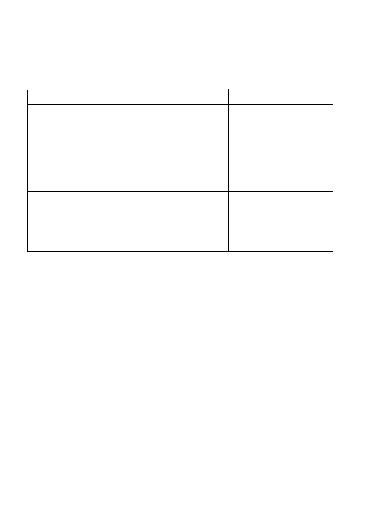
Input signals - Logic and current defining pins
Parameter
Data and strobe
Input voltage high
Input voltage low
Input capacitance
Input current
Clock
Input voltage high
Input voltage low
Input capacitance
Input current
Input frequency
Current setting pins
Input Signal RSA
Input current
Input Signal RSM
Input current
Input Signal RSC
Input current
Phase Detector Input Frequency
Notes
Min
Vdd-0.8
0
Vdd-0.8
0
Typ
80
32
12.8
1.0
Max
Vdd
0.8
10
10
Vdd
0.8
10
10
10
Unit
V
V
pF
µA
V
V
pF
µA
MHz
µA
µA
µA
MHz
Condition
Note 1
Note 2
Note 3
Note 5
1. The current set on pin RSA will be scaled up on chip by a factor of 3 to give the value of the auxiliary phase detector
output.
2. The current set on pin RSM will be scaled down on chip by a factor of 32 to provide the current
detector which gives the outputs
3. The current set on pin RSC will be scaled down on chip by a factor of 128 to provide the current
detector which gives the outputs
4. The voltage on each of the three current setting pins (RSA, RSM, RSC) is approximately 4V.
Therefore to give a typical current of 32µA on RSM a 125kΩ resistor connected between then pin and GND would be
required.
5. This is the maximum comparison frequency.
I
prop
I
comp
and
and
I
.
int
I
comp 2
.
I
to the main phase
bo
I
to the main phase
co
10
Page 12
DYNAMIC
Vdd = 5V ± 10%, Tamb = -40 to +85°C
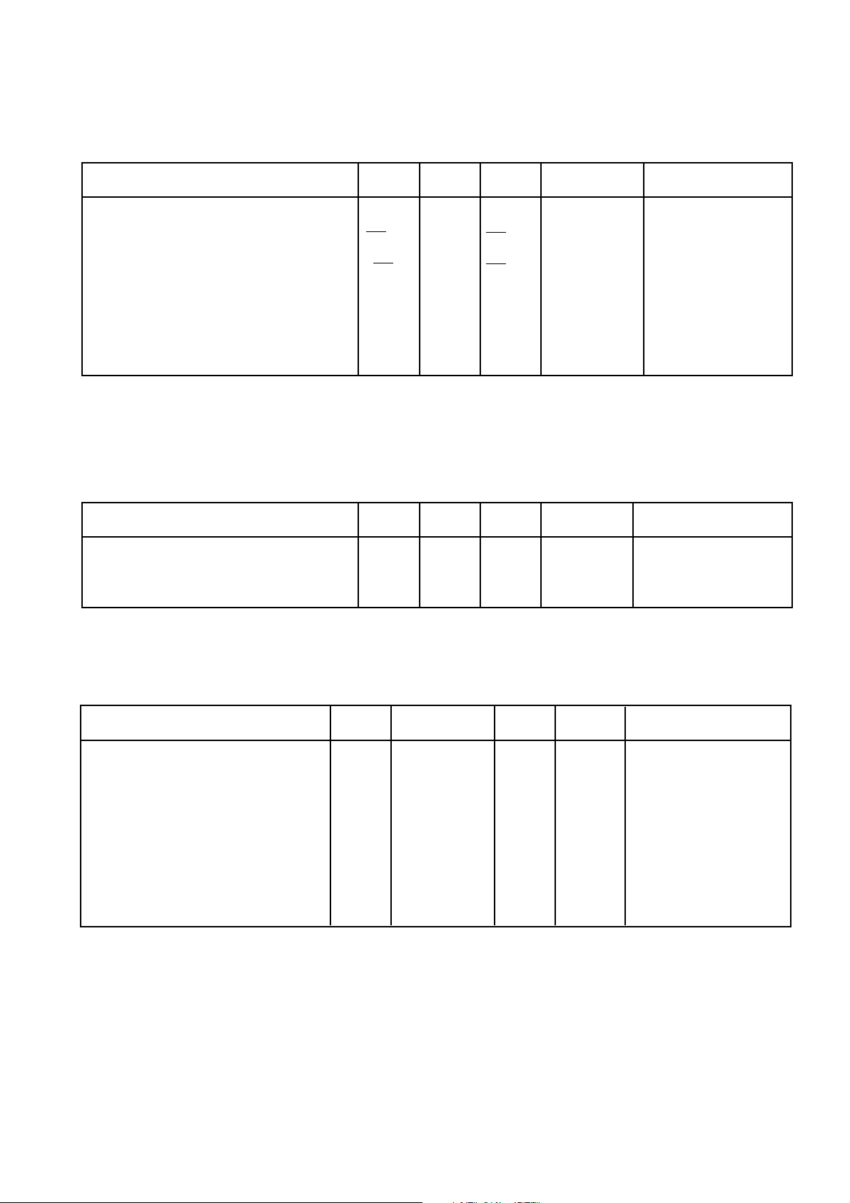
Output signals
NJ88C51
Parameter
Min
Modulus control - MOD1 MOD2
Output voltage high
Vdd + 0.3
2
Output voltage low
Vdd - 0.3
2
FIM clock to MOD1/MOD2 transition
Lock Detect LD
"In Lock" window t
Output voltage active high
L
Output voltage in active low
1
Vdd - 0.4
0
Notes
1. tL is one cycle of the input frequency applied to the RI input.
DYNAMIC
Vdd = 5V ± 10%, Tamb = -40 to +85°C
Output signals - Auxiliary synthesiser
Parameter
Output Signal - PDA
Up current
Down current
Tristate
Min
+225
-225
Typ
15
±1
Typ
+250
-250
Max
V
dd + 0.7
2
Vdd - 0.7
2
Vdd
0.4
Max
+275
-275
10
Unit
V
V
ns
Reference cycle
V
v
Unit
µA
µA
nA
Condition
Push-Pull output
OH = 10µA
I
IOL = -10µA
10pF load
Push-Pull output
Note 1
IOH = 0.5mA
IOL = 0.5mA
Condition
0<VPD<4.35V
0.65<VPD<5V
DYNAMIC
Vdd = 5V, Tamb = -40 to +85°C
Output signals - Main synthesiser, proportional output
Parameter
Output signal - PDP
Iprop(0) Up
Iprop(0) Down
Iprop(1) Up
Iprop(1) Down
see notes 1, 3 & 4
see notes 1, 3 & 4
see notes 2&3
see notes 2&3
Tristate
Notes
1. The typical value of
RSM, where
I
bo
=
I
2. The typical value of
3. The current output
I
PROP
(0)
is set by the programmed value of CN and the current
/ 32.
I
rsm
I
PROP
(1)
I
PROP
is specified between 100µA and 1mA.
is typically 32µA.
rsm
is set by the value of
Min
-10%
-10%
-10%
-10%
I
PROP
Typ
+Ibo.CN
-Ibo.CN
+Ibo.CN.2
-Ibo.CN.2
L+1
L+1
Max
+10%
+10%
+10%
+10%
50
(0)
and the programmed value of
Unit
µA
µA
µA
µA
Condition
PD<4.55V, Strobe=0V
0<V
0.45<VPD<5V, Strobe=0V
0<VPD<4.55V, Strobe=5V
0.45<VPD<5V, Strobe=5V
nA
I
set by the external resistor
rsm
L.
4. The output current is monotonic over the CN range 128-255. In standard operation CN is set at a value > 128.
11
Page 13
NJ88C51
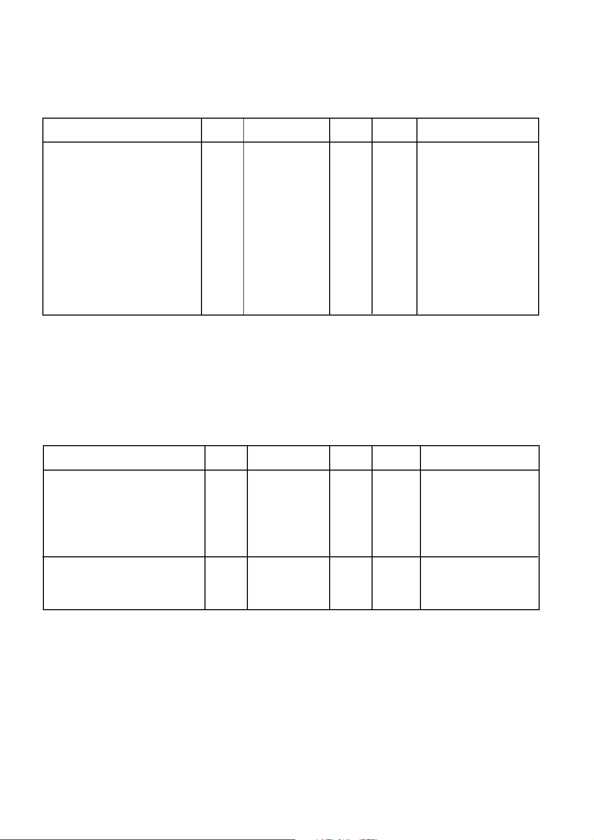
DYNAMIC
Vdd = 5V, Tamb = -40 to +85°C
Output signals - Main synthesiser, integral output
Parameter
Min
Typ
Output signal - PDI
I
INT Up
(1mA - 5mA)
IINT Down
(1mA - 5mA)
IINT Up
(5mA - 10mA)
IINT Down
(5mA - 10mA)
see notes 1&2
see notes 1&2
see notes 1&2
see notes 1&2
-10%
-10%
-10%
-10%
+Ibo.CN.2
-Ibo.CN.2
+Ibo.CN.2
-Ibo.CN.2
L+1
L+1
L+1
L+1
Tristate
Notes
1. The typical value of
2. The current output
is set by the value of
I
INT
is specified between 1mA and 10mA.
Iprop(1)
and the programmed value of K.
I
INT
DYNAMIC
Vdd = 5V, Tamb = -40 to +85°C
Output signals - Main synthesiser, under Fractional-N control
.K
.K
.K
.K
Max
+10%
+10%
+10%
+10%
50
Unit
mA
mA
mA
mA
nA
Condition
0<V
PD<4.45V, Strobe=5V
0.35<VPD<5V, Strobe=5V
0<VPD<4.3V, Strobe=5V
0.5<VPD<5V, Strobe=5V
Parameter
Min
Typ
Max
Unit
Output signal - PDP
COMP(0)
I
see notes 1&3
ICOMP (1)
see notes 2&3
-10%
-10%
Ico.Acc.
Ico.Acc.2
L+1
+10%
+10%
.
µA
µA
Output signal - PDI
COMP2
I
see notes 4&5
-10%
Ico.Acc.2
L+1
+10%
.K
µA
Notes
I
COMP
(0)
1. The typical value of
resistor RSC, where
2. The typical value of
3. The current output
I
I
COMP
I
COMP
is set by the fractional-N accumulator value Acc and the current
=
I
/128.
I
co
rsc
(1)
is set by the value of
is specified up to 12µA.
is typically 12.8µA.
rsc
I
COMP
(0)
and the programmed value of
4. The typical value of ICOMP2 is set by the value of ICOMP(1) and the programmed value of
5. The current output ICOMP2 is specified up to 180µA.
Condition
0<V
PD<4.55V, Strobe=0V
0<VPD<4.55V, Strobe=5V
0<VPD<4.55V, Strobe=5V
I
set by the external
rsc
L.
K.
12
Page 14
Vcc
NJ88C51
RF Vcc
Vcc
CONTROL
876
RF
PD
MC
SP8715
IC2
RF
VCCRSOUT
123
MAIN
RF out
5
VCE
4
UHF VCO
PRESCALER
Vcc
51918171615141312
AGND
MOD2
AVDD
FIM
734
LD
MOD1
NJ88C51
IC1
FIMB
DATA
120268
RSC
RSM
CKIN
STROBERIFIA
VDD
PDP
GND
RSA
9
11
PDI
PDA
10
Fig.8 Typical application
Vcc
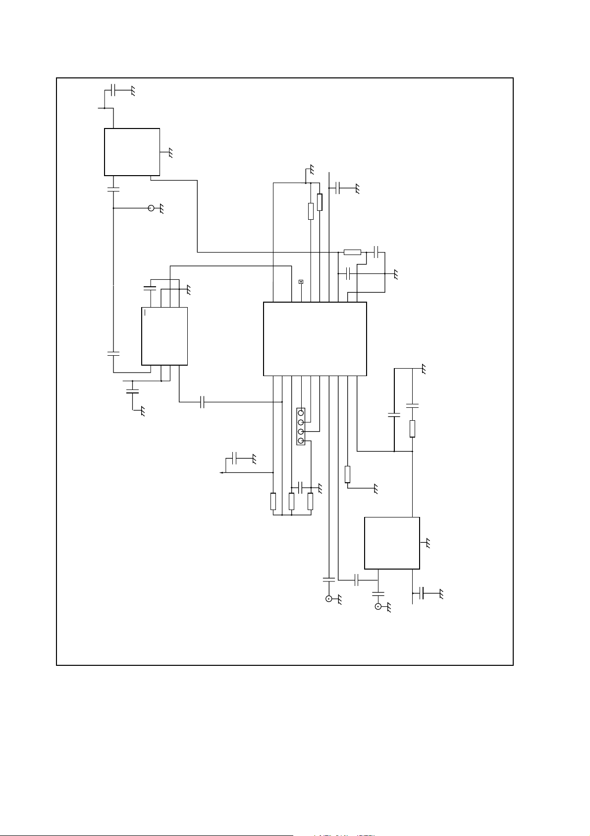
Fig.8 shows a typical application, using the NJ88C51 to
generate both VHF and UHF signals. External components
are kept to a minimum, requiring only bias, loop filter and
decoupling components. In many applications the UHF VCO
is a pre-assembled and tested module to suit the end equipment use, whereas the VHF design is likely to be discrete. The
circuit shown is suitable for operation up to 1.1GHz and uses
RF
CONTROL
Vcc
VHF VCO
Vcc
AUX
RF out
Reference in
a low power prescaler, the SP8715, feeding the NJ88C51 in
single ended mode. This requires a biasing network around
the differential input of the NJ88C51 to be used (pins 2 and 3).
Power supply and ground rails must have adequate
decoupling otherwise overall performance may be impaired.
13
Page 15

NJ88C51
14
Page 16

NJ88C51
15
Page 17

NJ88C51
HEADQUARTERS OPERATIONS
GEC PLESSEY SEMICONDUCTORS
Cheney Manor, Swindon,
Wiltshire SN2 2QW, United Kingdom.
Tel: (0793) 518000
Fax: (0793) 518411
GEC PLESSEY SEMICONDUCTORS
P.O. Box 660017
1500 Green Hills Road,
Scotts Valley, California 95067-0017,
United States of America.
Tel: (408) 438 2900
Fax: (408) 438 5576
This publication is issued to provide information only which (unless agreed by the Company in writing) may not be used, applied or reproduced for any purpose nor form part of any order or contract nor to be regarded
as a representation relating to the products or services concerned. No warranty or guarantee express or implied is made regarding the capability, performance or suitability of any product or service. The Company
reserves the right to alter without prior knowledge the specification, design or price of any product or service. Information concerning possible methods of use is provided as a guide only and does not constitute
any guarantee that such methods of use will be satisfactory in a specific piece of equipment. It is the user's responsibility to fully determine the performance and suitability of any equipment using such information
and to ensure that any publication or data used is up to date and has not been superseded. These products are not suitable for use in any medical products whose failure to perform may result in significant injury
16
or death to the user. All products and materials are sold and services provided subject to the Company's conditions of sale, which are available on request.
CUSTOMER SERVICE CENTRES
• FRANCE & BENELUX Les Ulis Cedex Tel: (1) 64 46 23 45 Fax : (1) 64 46 06 07
• GERMANY Munich Tel: (089) 3609 06-0 Fax : (089) 3609 06-55
• ITALY Milan Tel: (02) 66040867 Fax: (02) 66040993
• JAPAN Tokyo Tel: (03) 5276-5501 Fax: (03) 5276-5510
• NORTH AMERICA Scotts Valley, USA Tel (408) 438 2900 Fax: (408) 438 7023.
• SOUTH EAST ASIA Singapore Tel: (65) 3827708 Fax: (65) 3828872
• SWEDEN Stockholm, Tel: 46 8 702 97 70 Fax: 46 8 640 47 36
• UK, EIRE, DENMARK, FINLAND & NORWAY
Swindon Tel: (0793) 518510 Fax : (0793) 518582
These are supported by Agents and Distributors in major countries world-wide.
© GEC Plessey Semiconductors 1994 Publication No. DS3907 Issue No. 1.4 May 1994
 Loading...