

Page 1

THIS DOCUMENT IS FOR MAINTENANCE
PURPOSES ONLY AND IS NOT
RECOMMENDED FOR NEW DESIGNS
Page 2
DECEMBER 1993
NJ88C29
ADVANCE INFORMA TION
NJ88C29
FREQUENCY SYNTHESISER (MICROPROCESSOR SERIAL INTERFACE)
WITH NON-RESETTABLE COUNTERS
T
he NJ88C29 is a synthesiser circuit fabricated on the GPS
CMOS process and is capable of achieving high sideband
attenuation and low noise performance. It contains a reference
oscillator, 11-bit programmable reference divider, digital and
sample-and-hold comparators, 10-bit programmable ‘M’ counter,
7-bit programmable ‘A’ counter and the necessary control and
latch circuitry for accepting and latching the input data.
Data is presented serially under external control from a
suitable microprocessor. Although 28 bits of data are initially
required to program all counters, subsequent updating can be
abbreviated to 17 bits, when only the ‘A’ and ‘M’ counters require
changing.
The NJ88C29 is intended to be used in conjunction with a
two-modulus prescaler such as the SP8715 series to produce
a universal binary coded synthesiser for up to 1100MHz
operation. Operation from a 3.8V supply is also supported.
FEATURES
■
Low Power Consumption
■
High Performance Sample and Hold Phase Detector
■
Serial Input with Fast Update Feature
■
3.8V Operation
■
Fast Lock Up Time
■
SSOP Package
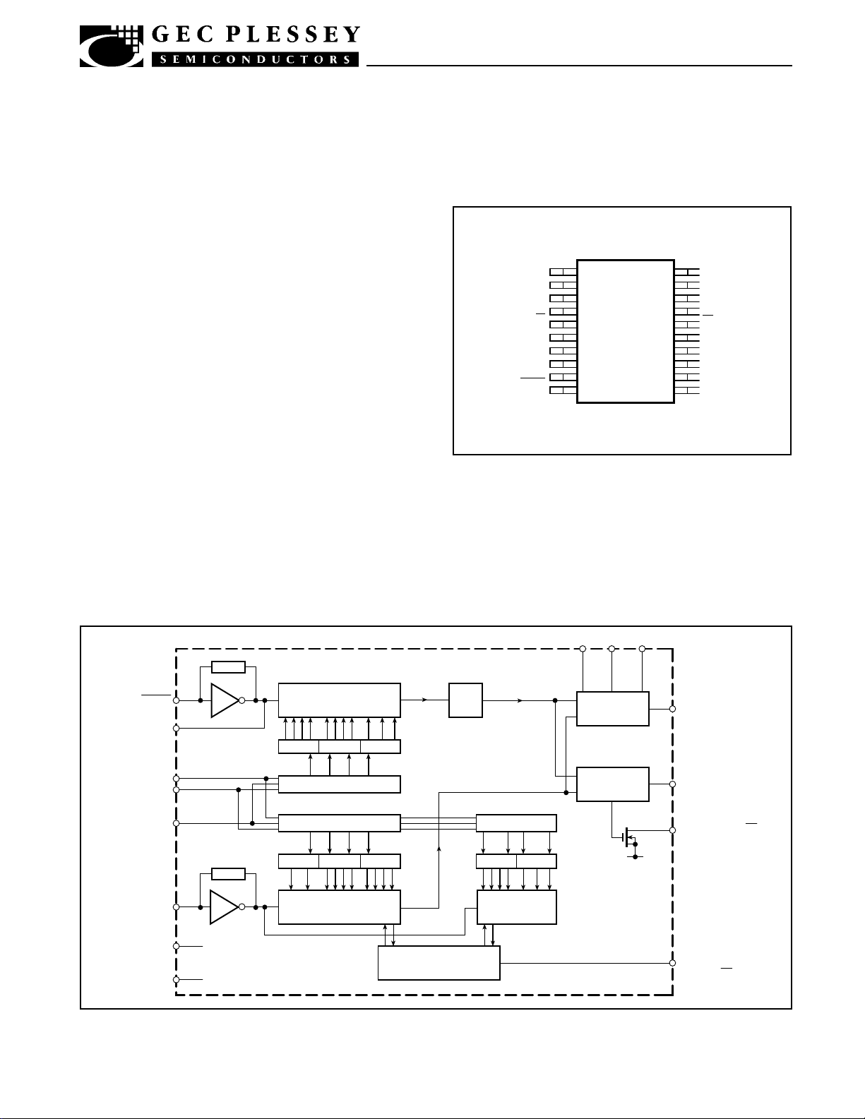
Fig.1 Pin connections - top view (not to scale)
ABSOLUTE MAXIMUM RATINGS
Supply voltage, VDD-V
Input voltage
Open drain output, pin 4
All other pins
Storage temperature
ORDERING INFORMATION
NJ88C29 KG/NPAS Shrunk Miniature Plastic DIL Package
PDA
PDB
NC
LD
F
IN
V
SS
V
DD
NC
OSC IN
OSC OUT
1
NJ88C29
10
SS
20
11
CH
RB
NC
MC
CAP
ENABLE
CLOCK
DATA
NC
NC
V
-0·3V to VDD+0·3V
SS
-55°C to +125°C
-0·75V to 7V
DS3889-1.6
NP20
7V
OSC IN
OSC OUT
DATA
ENABLE
CLOCK
F
IN
V
DD
V
SS
(9)
(10)
(13)
(15)
(14)
(5)
(7)
(6)
REFERENCE COUNTER
(11BITS)
LATCH 6 LATCH 7 LATCH 8
‘R’ REGISTER
‘M’ REGISTER
LATCH 1 LATCH 2 LATCH 3
‘M’ COUNTER
(10 BITS)
Fig.2 block diagram
÷2
CONTROL LOGIC
f
r
f
V
‘A’ REGISTER
LATCH 4 LATCH 5
‘A’ COUNTER
(7 BITS)
RB CAP CH
(19) (16) (20)
SAMPLE/HOLD
PHASE
DETECTOR
FREQUENCY/
PHASE
DETECTOR
(1)
PDA
(2)
PDB
(4)
LOCK DETECT (LD)
V
SS
MODULUS
(17)
CONTROL
OUTPUT (MC)
1
Page 3
NJ88C29
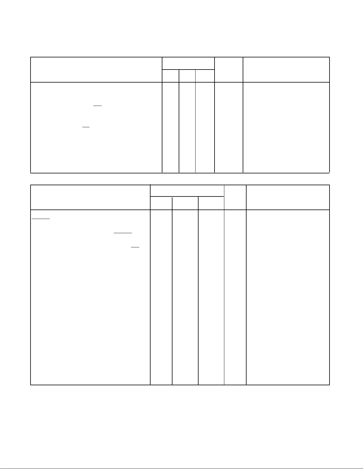
ELECTRICAL CHARACTERISTICS AT VDD = 3.8V
These characteristics are guaranteed over the following conditions, unless otherwise stated:
V
DC Characteristics
Characteristic Units Conditions
Supply current 3.0 5·0 mA f
Modulus Control Output (
High level 2.5 V I
Low level 0·4 V I
Lock Detect Output (
Low level 0·4 V I
Open drain pull-up voltage 7·0 V
PDB Output
High level 2.5 V I
Low level 0·4 V I
3-state leakage current ±100 nA
AC Characteristics
=3.8V ±0·4V. Temperature range = –15°C to +70°C
DD–VSS
MC)
LD)
Value
Min. Typ. Max.
0.6 0.94 mA f
, f
osc
, f
osc
SOURCE
= ImA
SINK
= 4mA
SINK
SOURCE
= 3mA
SINK
= 10MHz
FIN
= 4·096MHz
FIN
= ImA
= 3mA
0 to 3.8V
square
wave
Value
Characteristic Units Conditions
Min. Typ. Max.
OSC IN input level and FIN input level 12.8MHz AC-coupled sinewave
200
mV RMS
See note 4
Max. operating frequency, F
and OSC IN inputs Input squarewave VDD to VSS,
IN
20
MHz
25°C. See note 5.
Propagation delay, F
to modulus control MC See note 2
IN
30
Programming Inputs
Clock high time, t
Clock low time, t
CH
CL
Enable set-up time, t
Enable hold time, t
Data set-up time, t
Data hold time, t
EH
DS
DH
ES
0.5
0.5
0.2
0.2
0.2
0.2
Clock rise and fall times
High level threshold See note 1
Low level threshold See note 1
Hysteresis See note 1
0.4
1.23
1.8
50
t
CH
0.2
V
-0.24
DD
ns
µs
µs
µs
µs
µs
µs
µs
All timing periods
are referenced to
the negative
transition of the
clock waveform
See note 4
V
V
V
Phase Detector See note 3
V
V
ns
µA
Set by external conditions.
pF
plus packaging strays.
int
Ω
V
1.12
DD
500
7.0
100
80
–0.9
300
7.8
Positive going threshold, V
Negative going threshold, V
+
T
–
T
Digital phase detector propagation delay
RB current, I
RB
CAP/RB current gain, α Over RB current range.
5
6.3
Programming capacitor, CAP C
Output resistance, PDA, PDB
NOTES
1. Data, Clock and Enable inputs are high impedance Schmitt buffers without pull-up resistors; they are therefore not TTL compatible.
2. All counters have outputs directly synchronous with their respective clock rising edges.
3. The finite output resistance of the internal voltage follower and ‘on’ resistance of the sample switch driving this pin will add a finite time constant
to the loop. An external 1nF hold capacitor will give a maximum time constant of 5µs, typically; 1µs for the sample and hold amplifier.
4. The inputs to the device should be at logic ‘0’ when power is applied if latch-up conditions are to be avoided. This includes the signal/osc.
frequency inputs.
5. The minimum Fin period is governed by a time constant determined by the capacitance value on the CAP pin and the internal CAP discharge
resistance. Depending on the value of CAP, PLL performance may be degraded at frequencies below 20MHz - see AN112 for further details.
2
Page 4
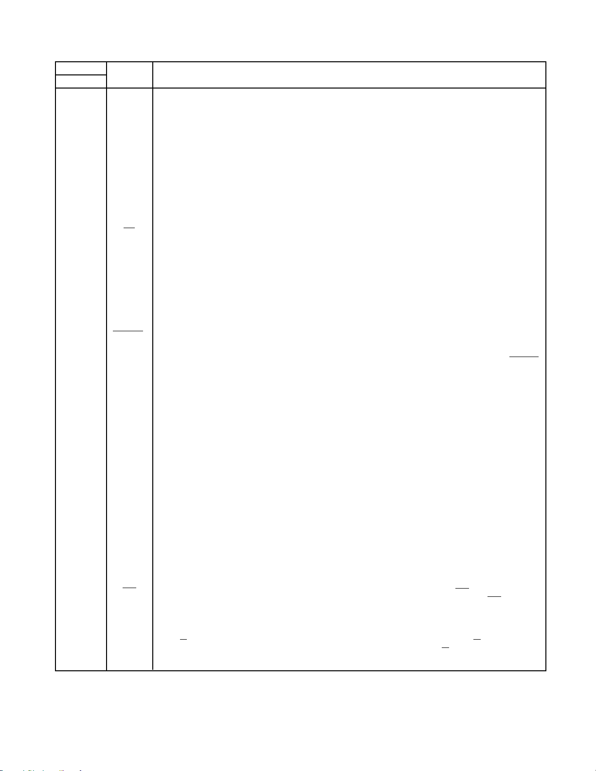
PIN DESCRIPTIONS
NJ88C29
Pin no.
NP
1
2
3
4
5
6
7
8
9,10
Name
PDA
PDB
NC
LD
F
IN
V
SS
V
DD
NC
OSC IN/
OSC OUT
Description
Analog output from the sample and hold phase comparator for use as a ‘fine’ error signal. Voltage
increases as fv (the output from the ‘M’ counter) phase lead increases; voltage decreases as fr (the
output from the ‘R’ counter) phase lead increases. Output is linear over only a narrow phase window,
determined by gain (programmed by RB). This pin is at (V
external loop filter amplifier biased to (VDD–VSS)/2. Ideally, V
window is centred between the thresholds, typically at 0·55(V
)/2 when the system is in lock, for an
DD–VSS
should be chosen such that the PDA
BIAS
DD–VSS
)
Three-state output from the phase/frequency detector for use as a ‘coarse’ error signal.
or fv leading: positive pulses with respect to the bias point V
f
v>fr
fv<fr or fr leading: negative pulses with respect to the bias point V
fv = fr and phase error within PDA window: high impedance.
M
(Minimum,
= 3 for correct function of PDB).
BIAS
BIAS
Not connected..
An open-drain lock detect output at low level when phase error is within PDA window (in lock); high
impedance at all other times.
The input to the main counters. It is normally driven from a prescaler, which may be AC-coupled or,
when a full logic swing is available, may be DC-coupled.
Negative supply (ground).
Positive supply.
Not connected.
These pins form an on-chip reference oscillator when a series resonant crystal is connected across
them. Capacitors of appropriate value are also required between each end of the crystal and ground
to provide the necessary additional phase shift. The addition of a 2·2kΩ resistor between pin 10 and
the crystal will improve stability. An external reference signal may, alternatively, be applied to
OSC IN.
This may be a low-level signal, AC-coupled, or if a full logic swing is available it may be DC-coupled.
The program range of the reference counter is 3 to 2047 in steps of 1, with the total division ratio being
twice the programmed value i.e., 6 to 4094 in steps of 2.
11
12
13
14
15
16
17
18
NC
NC
DATA
CLOCK
ENABLE
CAP
MC
NC
Not connected.
Not connected.
Information on this input is transferred to the internal data latches during the appropriate data read time
slot. DATA is high for a ‘1’ and low for a ‘0’. There are three data words which control the NJ88C29;
MSB is first in the order: ‘A’ (7 bits), ‘M’ (10 bits), ‘R’ (11 bits).
Data is clocked on the negative transition of the CLOCK waveform. If less than 28 negative clock
transitions have been received when the ENABLE line goes low (i.e., only ‘M’ and ‘A’ will have been
clocked in), then the ‘R’ counter latch will remain unchanged and only ‘M’ and ‘A’ will be transferred from
the input shift register to the counter latches. If 28 negative transitions have been counted, then the ‘R’
counter will be loaded with the new data.
When ENABLE is low, the DATA and CLOCK inputs are disabled internally. As soon as ENABLE is
high, the DATA and CLOCK inputs are enabled and data may be clocked into the device. The data is
transferred from the input shift register to the counter latches on the negative transition of the ENABLE
input and both inputs to the phase detector are synchronised to each other.
This pin allows an external capacitor to be connected in parallel with the internal ramp capacitor and
allows further programming of the device. (This capacitor is connected from CAP to V
Modulus control output for controlling an external dual-modulus prescaler.
MC will be low at the
SS
).
beginning of a count cycle and will remain low until the ‘A’ counter completes its cycle. MC then goes
high and remains high until the ‘M’ counter completes its cycle, at which point both ‘A’ and ‘M’ counters
MP+A
are reset. This gives a total division ratio of
, where P and P+1 represent the dual-modulus
prescaler values. The program range of the ‘A’ counter is 0–127 and therefore can control prescalers
with a division ratio up to and including ÷ 128/129. The programming range of the ‘M’ counter is 3-1023
>8 for correct PDA operation and, for correct operation with a prescaler, M>A. Where every
but M
possible channel is required, the minimum total division ratio N should be: N>
2
P
–P, where N = MP+A.
Not connected
3
Page 5
NJ88C29
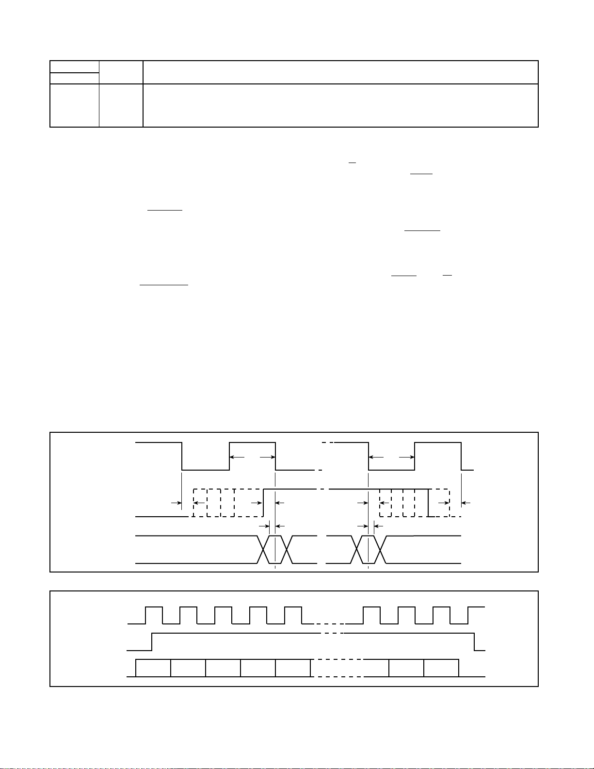
PIN DESCRIPTIONS (continued)
Pin no.
NP
19
20
Name Description
RB
CH
An external sample and hold phase comparator gain programming resistor should be connected
between this pin and V
SS
. I
300µA at V
RB
An external hold capacitor should be connected between this pin and VSS.
PROGRAMMING
Reference Divider Chain
The comparison frequency depends upon the crystal
oscillator frequency and the division ratio of th ‘R’ counter,
which can be programmed in the range 3 to 2047, and a fixed
divide by two stage.
f
osc
=
2x
fcomp
where
R
fosc
= oscillator frequency,
fcomp
= comparison frequency,
R
= ‘R’ counter ratio
For example, where the crystal frequency = 10MHz and a
channel spacing comparison frequency of 12·5kHz is required,
7
R
= = 400
10
2x12·5x10
3
Thus, the ‘R’ register would be programmed to 400 expressed
in binary. The total division ratio would then be 2X400 = 800
since the total division ratio of the ‘R’ counter plus the ÷ 2 stage
is from 6 to 4094 in steps of 2.
VCO Divider Chain
The synthesised frequency of the voltage controlled oscillator
(VCO) will depend on the division ratios of the ‘M’ and ‘A’
counters, the ratio of the external two-modulus prescaler
(
P/P+1
)and the comparison frequency .
The division ratio N =
where M is the ratio of the M counter in the range 3 to 1023
and
A
is the ratio of the ‘A’ counter in the range 1 to 127.
MP+A
,
= 3.8V.
DD
Note that M>A and
f
VCO
N
=
fcomp
For example, if the desired VCO frequency = 275MHz, the
comparison frequency is 12·5kHz and a two-modulus prescaler
of ÷ 64/65 is being used, then
6
275x10
N
= = 22x10
12·5x10
3
Now, N = MP+A, which can be rearranged as
3
N/P
= M+
A/P.
In our example we have P = 64, therefore
3
= M+
A
64
such that
22x10
64
M
= 343 and A/64 = 0.75.
Now, M is programmed to the integer part = 343 and A is
programmed to the fractional partx64 i.e., A = 0·75x64 = 48.
NB The minimum ratio
N
that can be used is
2
P
–P (4032 in our
example) for all contiguous channels to be available.
To check: N = 343x64+48 = 22000, which is the required
division ratio and is greater than 4032 ( =
2
P
–P).
When re-programming, the counters are changed only at
the zero state. There is no reset to zero, which means that the
synthesiser loop lock up time will be variable with respect to the
programming sequence timing. When only small changes in
frequency are required, the NJ88C29 non-resettable
synthesiser should achieve the shortest loop lock up times.
CLOCK
ENABLE
DATA
t
CH
t
EH
t
ES
t
DS
t
EH
t
DH
t
CL
t
ES
Fig. 3 Timing diagram showing timing periods required for correct operation
CLOCK
ENABLE
DATA
12
A
6
A
5
345
A
A
4
A
3
2
(15)26 (16)27 (17)28
(M2)R2(M1)R1(M0)R
0
Fig. 4 Timing diagram showing programming details
4
Page 6
PHASE COMPARATORS
Noise output from a synthesiser loop is related to loop gain:
K
K
VCO
PD
2π
N
K
, which is programmable with
PDA
α
I
RB
C
f
comp
CAP
C
.
Application Note AN112
EXT
K
. A smaller
SS
VCO
is
where
K
is the phase detector constant (volts/rad),
PD
the VCO constant (rad/sec-volt) and N is the overall loop
division ratio. When N is large and the loop gain is low, noise
may be reduced by employing a phase comparator with a high
gain. The sample and hold phase comparator in the NJ88C29
has a high gain and uses a double sampling technique to
reduce spurious outputs to a low level.
A standard digital phase/frequency detector driving a threestate output, PDB, provides a ‘coarse’ error signalto enable
fast switching between channels.
The PDB output is active until the phase error is within the
sample and hold phase detector window, when PDB becomes
high impedance. Phase-lock is indicated at this point by a low
level on
LD. The sample and hold phase detector provides a
‘fine’ error signal to give further phase adjustment and to hold
the loop in lock. An internally generated ramp, controlled by the
digital output from both the reference and main divider chains,
is sampled at the reference frequency to give the ‘fine’ error
signal, PDA. When in phase lock, this output would be typically
at the bias voltage set by the external loop filter amplifier; any
offset from this would be proportional to phase error.
The relationship between this offset and the phase error is
the phase comparator gain,
an external resistor, RB, and a capacitor, CAP. An internal
100pF capacitor is used in the sample and hold comparator.
Typically, the gain is given by:
K
=
PDA
where
C
= internal 100pF+
CAP
deals with this further.
A hold capacitor (CH) of non-critical value, which might be
typically 470pF, is connected from pin 18 to V
value
NJ88C29
is sufficient if the required sideband performance is not
high.The output from the sample and hold phase detector
should be combined with that of the coarse phase/frequency
detector and filtered to generate a single control voltage to
drive the VCO. The PDB gain is:
V
K
The stated minimum of 3 for the ‘M’ counter is true for the
PDB output only. To avoid race conditions in the internal phase
comparator counter for controlling the PDA timing, the minimum
division ratio for the ‘M’ counter should be 8 or more. Fig. 6
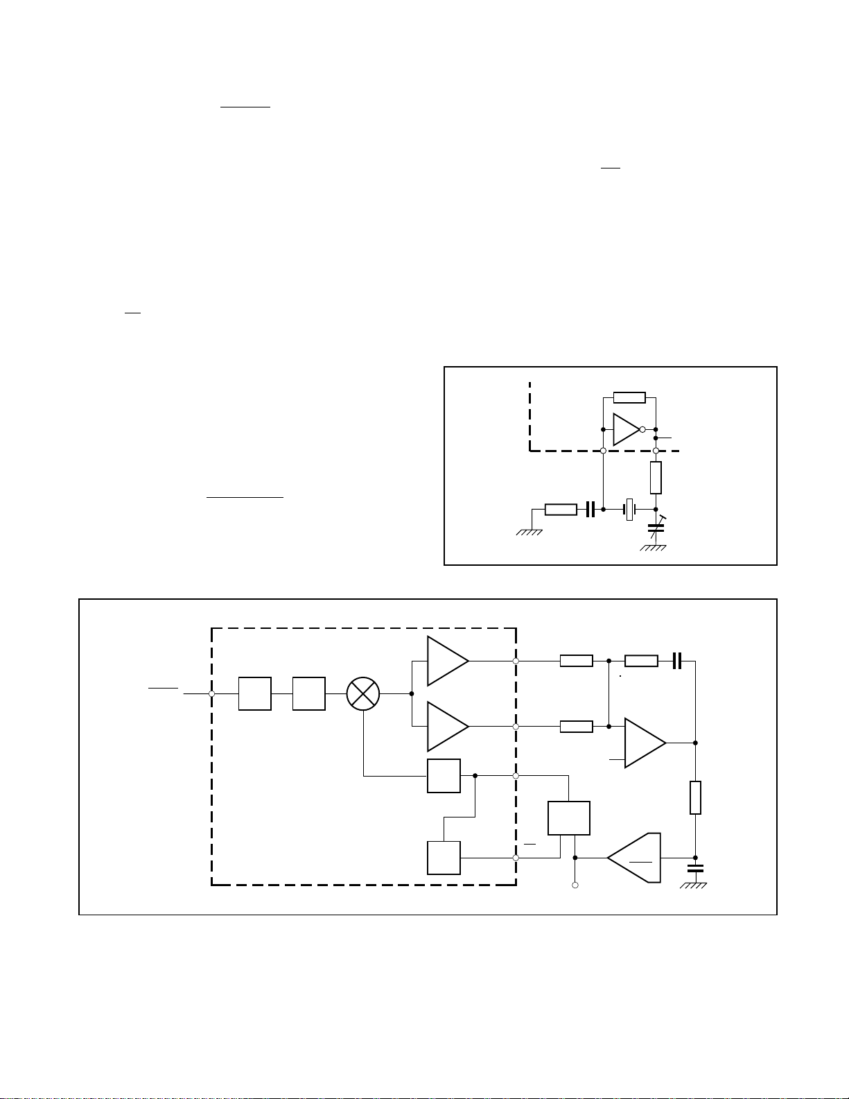
shows a typical NJ88C29 application.
CRYSTAL OSCILLATOR
When using the internal oscillator, the stability may be
enhanced at high frequencies by the inclusion of a resistor
between pin 10 (OSC OUT) and the other components, as
shown in Fig. 5. A value of between 220Ω and 2·2kΩ is
advised, depending on the crystal series resistance.
NJ88C29
100
Fig. 5 Suggested crystal oscillator circuit
DD
=
PDB
4π
910
SERIES
68p
2·2k
5 – 65p
OSC IN
K
PDA
9
–
÷2÷R
+
K
PDB
÷M
1
2
F
5
NJ88C29
17
÷A
MC
R1a
R1b
V
÷P/P+1
f
out
BIAS
in
C2
R2
-
+
R3
K
VCO
s
C3
Fig.6 NJ88C29 application circuit
5
Page 7
NJ88C29
PROGRAMMING/POWER UP
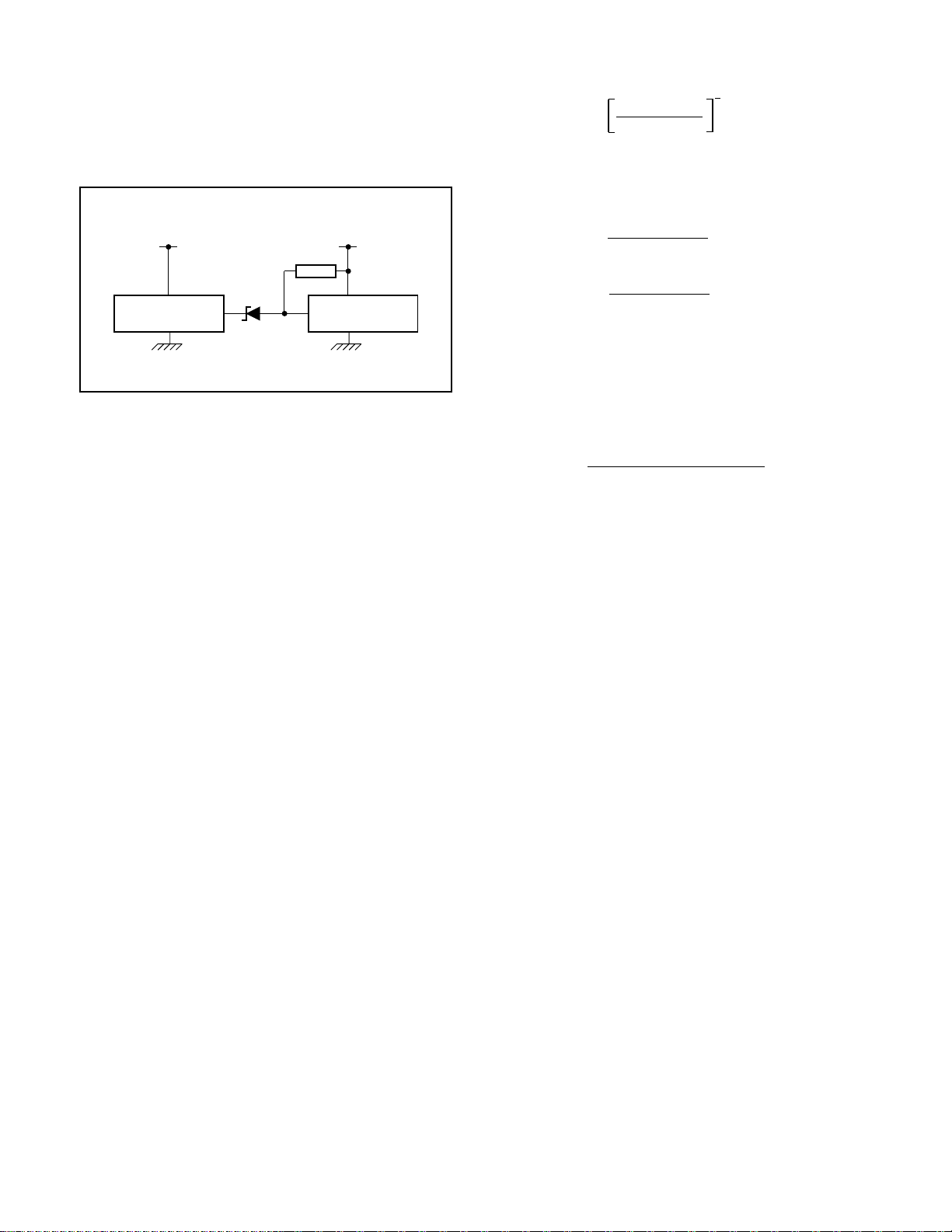
All data and signal input pins should have no input applied
to them prior to the application of V
may occur. When programming the device, DATA, ENABLE
and CLOCK pins must not exceed VDD as lock up times may be
compromised. A suggested interface to prevent this situation
is shown in Fig. 7.
V
(> VDD)
CC
PROGRAMMING
DEVICE
1N5711
Fig. 7 Suggested programming circuit
, as otherwise latch-up
DD
V
2k
DD
NJ88C29
LOOP EQUATIONS
1
K
VCO KPD
N R C2 C3 R
K
VCO KPD R2
= [ ωo (2ζ+R)]
3
N
ω0 (1+2ζR)
K
K
VCO KPD
VCO KPD
N R
( R + 2 ζ)
( 2 ζ+ R )
ω
where
w0 =
ζ = [ (
C3R
R
=
2
C
=
2
ω
= loop natural frequency
0
ζ = damping factor
R = ratio of real pole to ω
N
= MP+
A
or
provided
PDA window =
KPD = K
KPD = K
R
1a >> R1b
V
DD
PDA
PDB
–[ (V
/
R
/
R
+)+(V
T
2π
1a
1b
Further details are to be found in Application Note AN112.
3
3
) / { (
NC3 R
–1
2
0
0
–)]
N f
T
comp
K
PDA
2
ω
3
0
) –1}] / 2R
6
Page 8

NJ88C29
7
Page 9
NJ88C29
5.21/5.38
(0.205/0.212)
1.676/1.778
(0.066/0.070)
20
1
(0.0256)
(0.278/0.289)
PIN 1 IDENT
0.6502
REF
7.061/7.341
11
10
0.254/0.381
(0.010/0.015)
7.764/7.899
(0.301/0.311)
1.727/1.981
(0.065/0.078)
0.559/0.940
(0.022/0.037)
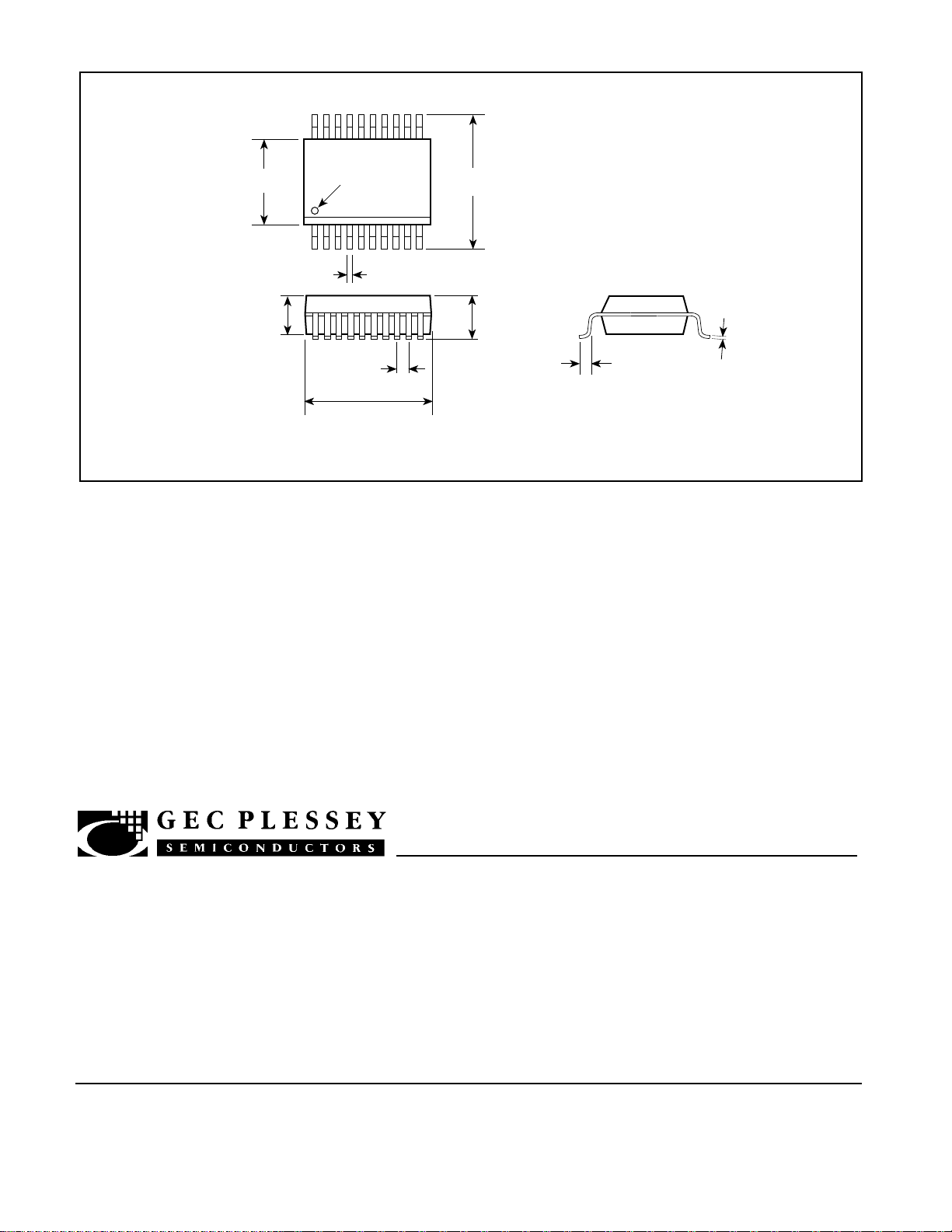
20 - LEAD SHRUNK MINIATURE PLASTIC DIL - NP20
0.127/0.229
(0.005/0.009)
HEADQUARTERS OPERATIONS
GEC PLESSEY SEMICONDUCTORS
Cheney Manor, Swindon,
Wiltshire SN2 2QW, United Kingdom.
Tel: (0793) 518000
Fax: (0793) 518411
GEC PLESSEY SEMICONDUCTORS
P.O. Box 660017
1500 Green Hills Road,
Scotts Valley, California 95067-0017,
United States of America.
Tel: (408) 438 2900
Fax: (408) 438 5576
This publication is issued to provide information only which (unless agreed by the Company in writing) may not be used, applied or reproduced for any purpose nor form part of any order or contract nor to be regarded
as a representation relating to the products or services concerned. No warranty or guarantee express or implied is made regarding the capability, performance or suitability of any product or service. The Company
reserves the right to alter without prior knowledge the specification, design or price of any product or service. Information concerning possible methods of use is provided as a guide only and does not constitute
any guarantee that such methods of use will be satisfactory in a specific piece of equipment. It is the user's responsibility to fully determine the performance and suitability of any equipment using such information
and to ensure that any publication or data used is up to date and has not been superseded. These products are not suitable for use in any medical products whose failure to perform may result in significant injury
or death to the user. All products and materials are sold and services provided subject to the Company's conditions of sale, which are available on request.
CUSTOMER SERVICE CENTRES
• FRANCE & BENELUX Les Ulis Cedex Tel: (1) 64 46 23 45 Fax : (1) 64 46 06 07
• GERMANY Munich Tel: (089) 3609 06-0 Fax : (089) 3609 06-55
• ITALY Milan Tel: (02) 66040867 Fax: (02) 66040993
• JAPAN Tokyo Tel: (03) 5276-5501 Fax: (03) 5276-5510
• NORTH AMERICA Integrated Circuits and Microwave Products Scotts Valley, USA
Tel (408) 438 2900 Fax: (408) 438 7023.
Hybrid Products, Farmingdale, USA Tel (516) 293 8686 Fax: (516) 293 0061.
• SOUTH EAST ASIA Singapore Tel: (65) 3827708 Fax: (65) 3828872
• SWEDEN Stockholm, Tel: 46 8 702 97 70 Fax: 46 8 640 47 36
• UK, EIRE, DENMARK, FINLAND & NORWAY
Swindon Tel: (0793) 518510 Fax : (0793) 518582
These are supported by Agents and Distributors in major countries world-wide.
© GEC Plessey Semiconductors 1993 Publication No. DS3889 Issue No. 1.6 December 1993
8
 Loading...