

Page 1

INTEGRATED CIRCUITS
NE83C92
Low-power coaxial Ethernet transceiver
Product specification
IC19 Data Handbook
1995 May 01
Page 2
Philips Semiconductors Product specification
NE83C92Low-power coaxial Ethernet transceiver
DESCRIPTION
The NE83C92 is a low power BiCMOS coaxial transceiver interface
(CTI) for Ethernet (10base5) and Thin Ethernet (10base2) local area
networks. The CTI is connected between the coaxial cable and the
Data Terminal Equipment (DTE) and consists of a receiver,
transmitter, receive-mode collision detector, heartbeat generator and
jabber timer (see Block Diagram). The transmitter output connects
directly to a doubly terminated 50Ω cable, while the receiver output,
collision detector output and transmitter input are connected to the
DTE through isolation transformers. Isolation between the CTI and
the DTE is an IEEE 802.3 requirement that can be met on signal
lines by using a set of pulse transformers. Power isolation for the
CTI is achieved using DC-to-DC conversion through a power
transformer.
The part is fully pin compatible with the industry standard 8392, but
has substantially lower current consumption, is fully compliant with
the IEEE802.3 standard, and has additional features such as
automatic selection between AUI and coaxial connections, and
requires no external pull-down resistors for local integrated MAU
application.
The NE83C92 is manufactured on an advanced BiCMOS process
and is available with PLCC package which make it ideally suited to
lap-top personal computers or systems where low power
consumption, limited board space and jumperless design is
required. Refer to selection flow chart for optimal application.
FEA TURES
•Fully compliant with Ethernet II, IEEE 802.3 10BASE-5 and
10BASE-2, and ISO 8802/3 interface specifications
•100% drop-in compatible with industry standard 8392 sockets
•Optimal implementation can use 1 Watt DC-DC converter and
reduces external part count (local/integrated MAU requires no
external pull-down resistors).
•High efficiency AUI drivers automatically power-down under idle
conditions to minimize current consumption
•Automatically disabling AUI drivers when disconnecting coax
cable, allowing hardwiring of AUI connection and local/integrated
CTI connection
•Smart squelch on data inputs eliminates false activations
•Advanced BiCMOS process for extremely low power operation
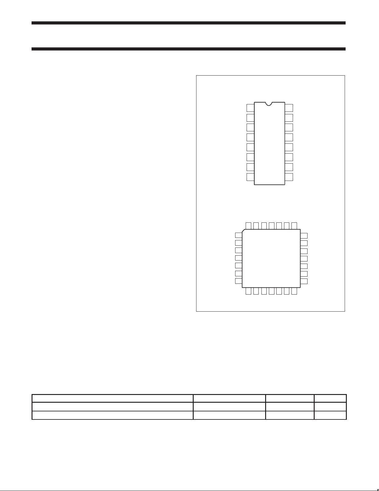
PIN CONFIGURATION
N Packages
16
CD+
CD–
RX+
V
V
RX–
TX+
TX–
1
2
3
4
EE
5
EE
6
7
8
CDS
15
TXO
14
RXI
V
13
EE
12
RR–
11
RR+
10
GND
9
HBE
A PACKAGE
RXI
RX+
CD–
CD+
V
5
EE
V
6
EE
V
7
EE
V
8
EE
V
9
EE
V
10
EE
V
11
EE
12 13 14 15 16 17 18
TX–
TX+
RX–
1234
CDS
HBE
TXO
GND
N/C
GND
262728
25
24
23
22
21
20
19
RR+
SD00308
V
EE
V
EE
V
EE
V
EE
V
EE
V
EE
RR–
Figure 1. Pin Configurations
•Available in 16-pin DIP, and 28-pin PLCC packages
•Expanded version (NE83Q93) with 5 LED status drivers is
available for repeater and advanced system applications
•Full ESD protection
•Power-on reset prevents glitches on coaxial cable during
power-up
ORDERING INFORMATION
DESCRIPTION TEMPERATURE RANGE ORDER CODE DWG #
16-Pin Plastic Dual In-Line Package
28-Pin Plastic Leaded Chip Carrier
1995 May 01 853-1736 15180
2
0 to +70°C
0 to +70°C
NE83C92N SOT38-4
NE83C92A SOT261-3
Page 3
Philips Semiconductors Product specification
NE83C92Low-power coaxial Ethernet transceiver
PIN DESCRIPTIONS
PIN NO.
N PKG
1
2
3
6
7
8
9 15 HBE
11
12
14 26 RXI
15 28 TXO
16 1 CDS
10
4
5
13
NOTE:
1. The IEEE 802.3 name for CD is CI; for RX is DI; for TX is DO.
PIN NO.
PLCC
12
13
14
18
19
16
17
5 to 11
20 to 25 V
SYMBOL DESCRIPTION
2
3
4
CD+
CD–
RX+
RX–
TX+
TX–
RR+
RR–
GND Positive Supply Pin.
Collision Outputs. Balanced differential line driver outputs which send a 10MHz signal to the DTE in
the event of a collision, jabber interrupt or heartbeat test. External pull-down resistors are optional with
local/integrated MAU application.
Receiver Outputs. Balanced differential line driver outputs which send the received signal to the DTE.
External pull-down resistors are optional with local/integrated MAU application.
Transmitter Inputs. Balanced differential line receiver inputs which accept the transmission signal from
the DTE and apply it to the coaxial cable at TXO, once it meets Tx squelch threshold.
Heartbeat Enable. The heartbeat function is disabled when this pin is connected to VEE and enabled
when connected to GND or left floating.
External Resistor. A 1kΩ (1%) resistor connected between these pins establishes the signaling current
at TXO.
Receiver Input. This pin is connected directly to the coaxial cable. Received signals are equalized,
amplified, and sent to the DTE through the RX± pins, once it meets Rx squelch threshold.
Transmitter Output. This pin is connected directly (Thin Ethernet) or through an external isolating
diode (Ethernet) to the coaxial cable.
Collision Detect Sense. Ground sense connection for the collision detection circuitry. This pin should
be connected directly to the coaxial cable shield for standard Ethernet operation.
Negative Supply Pins.
EE
1995 May 01
3
Page 4
Philips Semiconductors Product specification
NE83C92Low-power coaxial Ethernet transceiver
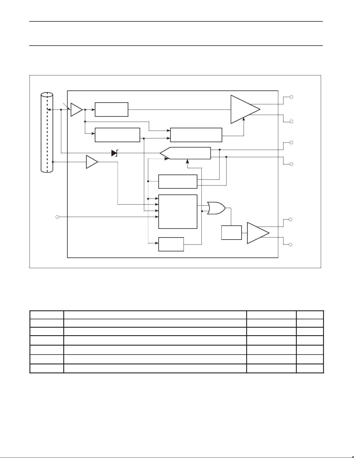
BLOCK DIAGRAM
COAX
CABLE
RXI
BUFFER
EQUALIZER
4–POLE BESSEL
LOW PASS FILTER
TXO
CDS
SENSE
BUFFER
HEARTBEAT ENABLE
RECEIVER
AC–DC SQUELCH
TRANSMITTER
TRANSMITTER
SQUELCH
COLLISION
COMPARATOR
&
HEARTBEAT
GENERATOR
JABBER
TIMER
RECEIVER
LINE
DRIVER
10MHz
OSC
LINE
DRIVER
DTE
INTERFACE
RECEIVE
PAIR
(RX+, RX–)
TRANSMIT
PAIR
(TX+, TX–)
COLLISION
PAIR
(CD+, CD–)
SD00274
Figure 2. Block Diagram
ABSOLUTE MAXIMUM RATINGS
SYMBOL PARAMETER RATING UNIT
V
EE
V
IN
T
STG
T
SOLD
T
J
θ
JA
NOTE:
1. 100% measured in production.
Supply voltage
Voltage at any input
Storage temperature range –65 to +150
Lead soldering temperature (10sec.) +300
Recommended max junction temperature
Thermal impedance (N and A packages) 60
2. The junction temperature is calculated from the following expression:
TJ = TA + θ
where
[(VEE x 0.015 x n
JA
TA = Ambient temperature in °C.
θJA = Thermal resistance of package.
= Normal operating supply voltage in volts.
V
EE
n
= Percentage of duty cycle idle
IDL
= Percentage of duty cycle receiving
n
RX
n
= Percentage of duty cycle transmitting
TX
1
1
2
) + (VEE x 0.018 x nRX) + (VEE x 0.066 x nTX)]
IDL
–12 V
0 to –12 V
+150
°C
°C
°C
°C/W
1995 May 01
4
Page 5

Philips Semiconductors Product specification
NE83C92Low-power coaxial Ethernet transceiver
ELECTRICAL CHARACTERISTICS
4
MAX
CD
1,2
. No external isolation
Without external
pull-down resistors
Measured by applying
DC voltage at RXI
Measured as DC
voltage at RXI
V
RXI
TX+
and V
are the max and min voltages at TXO with a 25Ω load between TXO and
MIN
.
LIMITS
–7.5 V
–70 –85 mA
= 0V –2 +25 µA
RXI
= 0V +1 +3 µA
CDS
+2.4 V
EE
+1.6 V
EE
= 0V +10 µA
HBE
HBE
= V
EE
–30 µA
–37 –45 mA
±28 ±I
= –10V –250 +250 µA
TXO
TDC
–3.7 V
–1450 –1530 –1580 mV
(CDS = 0V)
–3.5 V
±600 ±1100 mV
±40 mV
average DC
(CDS = 0V)
– V
) peak –175 –225 –275 mV
TX–
–150 –250 –350 mV
1 2 pF
6 kΩ
mA
VEE = –9V ±6%; TA = 0°C to +70°C unless otherwise specified
SYMBOL PARAMETER TEST CONDITIONS MIN TYP MAX UNIT
V
UVL
Under voltage lockout. Transceiver disabled for
|VEE| < |V
UVL
|
Supply current idle –15 –20 mA
I
I
I
CDS
V
I
TDC
I
I
TX10
V
TCOM
V
V
V
V
V
V
V
R
C
R
R
R
EE
RXI
IH
V
IL
I
IH
I
IL
TAC
CD
DIS
OD
OB
OC
RS
TS
RXI
RXI
TXO
AUIZ
TX
Supply current transmitting (without collision)
Receive input bias current V
Cable sense input bias current V
HBE input HIGH voltage V
HBE input LOW voltage V
HBE input HIGH current V
HBE input LOW current V
Transmit output DC current level
Transmit output AC current level
3
3
Transmit current V
Transmitter output voltage compliance
Collision threshold
5
AUI disable voltage at RXI
Differential output voltage – non idle at RX± and
6
CD±
Differential output voltage imbalance – idle at
RX± and CD±
7
Output common mode voltage at RX± and CD± RXI = 0V –4.0 –5.5 –7.0 V
Receiver squelch threshold
Transmitter squelch threshold (V
Shunt resistance at RXI non–transmitting 100 kΩ
Input capacitance at RXI
8
Shunt resistance at TXO transmitting 7.5 10 kΩ
Differential impedance at RX± and CD± with no
coaxial cable connected
Differential impedance at TX± 20 kΩ
NOTES:
1. Currents flowing into device pins are positive. All voltages are referenced to ground unless otherwise specified. For ease of interpretation,
the parameter limit that appears in the MAX column is the largest value of the parameter, irrespective of sign. Similarly, the value in the MIN
column is the smallest value of the parameter, irrespective of sign.
2. All typicals are for V
3. I
is measured as (V
TDC
GND. I
4. The TXO pin shall continue to sink at least I
is measured as (V
TAC
5. Collision threshold for an AC signal is within 5% of V
= –9V and TA = 27°C.
EE
+ V
MAX
)/(2 x 25) where V
MIN
– V
MAX
)/(2 x 25).
MIN
min when the idle (no signal) voltage on this pin is –3.7V .
TDC
6. Measured on secondary side of isolation transformer. The transformer has a 1:1 turns ratio with an inductance between 30 and 100µH at
5MHz.
7. Measured as the voltage difference between the RX pins or the CD pins with the transformer removed.
8. Not 100% tested in production.
1995 May 01
5
Page 6

Philips Semiconductors Product specification
NE83C92Low-power coaxial Ethernet transceiver
TIMING CHARACTERISTICS
V
= –9V ±6%; TA = 0 to 70°C, unless otherwise specified1. No external isolation diode on TXO.
EE
LIMITS
SYMBOL PARAMETER TEST CONDITIONS MIN TYP MAX UNIT
t
RON
t
RD
t
RR
t
RF
t
OS
t
RJ
t
RHI
t
RM
t
TST
t
TD
t
TR
t
TF
t
TM
t
TS
t
TON
t
TOFF
t
CON
t
COFF
t
CHI
f
CD
t
CP
t
HON
t
HW
t
JA
t
JR
Receiver start up delay RXI to RX± (Figure 5)
First received bit on RX±
First validly timed bit on RX± t
Receiver prop. delay RXI to RX± V
Differential output rise time on RX± and CD±
Differential output fall time on RX± and CD±
2,3
2,3
Differential output settling time on RX± and CD±
to VOB = 40mV2 (see Figure 6)
V
= –2V peak 3 5 bits
RXI
+2 bits
RON
= –2V peak 20 50 ns
RXI
5 7 ns
5 7 ns
1 µs
Receiver and cable total jitter ±2 ±6 ns
Receiver high to idle time Measured to +210mV 200 850 ns
Rise and fall time matching on RX± and CD± tRF – t
Transmitter start-up delay TX± to TXO (Figure 7)
First transmitted bit on TXO
VTX± = –1V peak 1 2 bits
RR
First validly timed bit t
Transmitter prop delay TX± to TXO
(see Figure 7)
VTX± = 1V peak 5 20 50 ns
0.1 ±2 ns
+ 2 bits
TST
Transmitter rise time 10% to 90% (see Figure 7) 20 25 30 ns
Transmitter fall time 10% to 90% (see Figure 7) 20 25 30 ns
tTF – tTR mismatch
Transmitter added skew
Transmitter turn on pulse width (see Figure 7) V
5
4,5
= 1V peak 10 35 ns
±
TX
0 ±2 ns
0 ±2 ns
Transmitter turn off pulse width (see Figure 7) VTX± = 1V peak 125 200 ns
Collision turn on delay (see Figure 8) 0V to –2V step at RXI 13 bits
Collision turn off delay (see Figure 8) –2V to 0V step at RXI 16 bits
Collision high to idle time (see Figure 8) Measured to +210mV 200 850 ns
Collision frequency (see Figure 8) 8.5 10 11.5 MHz
Collision signal pulse width (see Figure 8) 35 70 ns
Heartbeat turn on delay (see Figure 9) 0.6 1.6 µs
Heartbeat test duration (see Figure 9) 0.5 1.5 µs
Jabber activation delay measured from TX± to
CD± (see Figure 10)
Jabber reset delay measured from TX± to CD±
(see Figure 10)
20 60 ms
250 650 ms
NOTES:
1. All typicals are for V
2. Measured on secondary side of isolation transformer (see Figure 4). The transformer has a 1:1 turn ratio with an inductance between 30
= –9V and TA = 27°C.
EE
and 100µH at 5MHz.
3. The rise and fall times are measured as the time required for the differential voltage to change from –225mV to +225mV, or +225mV to
–225mV, respectively.
4. Difference in propagation delay between rising and falling edges at TXO.
5. Not 100% tested in production.
1995 May 01
6
Page 7

Philips Semiconductors Product specification
NE83C92Low-power coaxial Ethernet transceiver
FUNCTIONAL DESCRIPTION
The NE83C92 is a low power BiCMOS coaxial Ethernet transceiver
which complies with the IEEE 802.3 specification and offers the
following features:
1. Low current consumption of typically 15mA when idling and
70mA while transmitting and no collision allows smaller DC-DC
converter to be used for the isolated power supply. (No external
pull-down resistors.)
2. Automatic selection of the AUI connector (for remote MAU)
instead of the direct local (Thin) coaxial connection is possible by
automatically placing the AUI drivers in high-impedance state
when the local coaxial cable is disconnected. This eliminates the
need for changing a jumper position on the Ethernet board when
selecting either one of the connections. (Automatic selection of
the local (Thin) connection is done by disconnecting the AUI
cable and reconnecting the local coaxial one, which allows the
NE83Q92 to automatically activate itself.)
3. High-efficiency AUI drivers for the RX± and CD± ports
automatically power down when idling and are powered up when
a receive signal is detected. This is very important/useful for
power sensitive applications such as lap-top computers or
PCMCIA cards.
4. The NE83C92 advanced AUI driver (RX± and CD±) design does
require external pull-down resistors (500Ω) to drive a terminated
(78Ω) AUI cable. However, these drivers will operate correctly
without the external resistors for integrated/local MAU
applications where no AUI cable is used. Hence, they can be
retro-fitted into existing 8392 designs with or without external
pull-down resistors depending on the application. An extra
current of 7mA/output (for 500Ω resistors) would be generated,
by these resistors, regardless of whether the transceiver is idle
or responding to traffic.
Receiver Functions
The receiver consists of an input buffer , a cable equalizer, a 4-pole
Bessel low pass filter, a squelch circuit and a differential line driver.
The buffer provides high input resistance and low input capacitance
to minimize loading and reflections on the coaxial cable.
The equalizer is a high pass filter that compensates for the low pass
effect of the coaxial cable and results in a flatband response over all
signal frequencies to minimize signal distortion.
The 4-pole Bessel low pass filter extracts the average DC voltage
level on the coaxial cable for use by the receiver squelch and
collision detection circuits.
The receiver squelch circuit prevents noise on the coaxial cable
from falsely triggering the receiver in the absence of a true signal.
At the beginning of a packet, the receiver turns on when the DC
level from the low pass filter exceeds the DC squelch threshold and
the received packet has started with a 01 bit sequence with
acceptable timing parameters. For normal signal levels this will take
less than 500ns, or 5 bits. However, at the end of a packet, a fast
receiver turn off is needed to reject both dribble bits on the coaxial
cable and spurious responses due to settling of the on-chip
bandpass filter. This is accomplished by an AC timing circuit that
disables the receiver if the signal level on the coaxial cable remains
high for typically 250ns and only enables the receiver again after
approximately .5µs. Figures 5 and 6 illustrate receiver timing.
The differential line driver provides typically ±
DTE with less than 7ns rise and fall times. When in idle state (no
received signal) its outputs provide <20mV differential voltage offset
to minimize DC standing current in the isolation transformer.
900mV signals to the
Transmitter Functions
The transmitter has differential inputs and an open collector current
driver output. The differential input common mode voltage is
established by the CTI and should not be altered by external
circuitry. Controlled rise and fall times of 25ns (±
higher harmonic components in the transmitted spectrum, while
matching of these rise and fall times to typically 2ns minimizes
signal jitter. The drive current levels of the CTI are set by an on-chip
bandgap voltage reference and an external 1% resistor. An on-chip
isolation diode is provided to reduce the transmitter’s coaxial cable
load capacitance. For Thin Ethernet applications, no further external
isolation diode is required, since the NE83C92 meets the capacitive
loading specifications. For Ethernet applications a further external
diode should be added to reduce loading capacitance.
The transmitter squelch circuit ensures that the transmitter can only
be enabled if the transmitted packet begins with a 01 bit sequence
where the negative-going differential signals are typically greater
than 225mV in magnitude and 25ns in duration.
The transmitter will be disabled at the end of a packet if there are no
negative going signals of greater than 225mV for more than typically
150ns. Figure 7 illustrates transmitter timing.
5ns) minimize
Collision Functions
The collision detection scheme implemented in the NE83C92 is
receive mode detection, which detects a collision between any two
stations on the network with certainty at all times, irrespective of
whether or not the local DTE is producing one of the colliding
signals. This is the only detection scheme allowed by the IEEE
802.3 standard for both repeater and non-repeater nodes.
The collision circuitry consists of the 4-pole Bessel low pass filter, a
comparator, a precision voltage reference that sets up the collision
threshold, a heartbeat generator, a 10MHz oscillator, and a
differential line driver .
The collision comparator monitors the DC level at the output of the
low pass filter and enables the line driver if it is more negative than
the collision threshold. A collision condition is indicated to the DTE
by a 10MHz oscillation signal at the CD outputs and typically occurs
within 700ns of the onset of the collision. The collision signal begins
with a negative-going pulse and ends with a continuous high-to-idle
state longer than 170ns. Figure 8 illustrates collision timing.
At the end of every transmission, the heartbeat generator creates a
pseudo collision to ensure that the collision circuitry is properly
functioning. This pseudo collision consists of a 1µs burst of 10MHz
oscillation at the line driver outputs approximately 1µs after the end
of the transmission. The heartbeat function can be disabled
externally by connecting the HBE (heartbeat enable) to V
allows the CTI to be used in repeater applications. Figure 9
illustrates heartbeat timing.
EE
. This
Jabber Functions
The jabber timer monitors the transmitter and inhibits transmission if
it is active for longer than typically 30ms. The jabber circuit then
enables the collision outputs for the remainder of the data packet
and for typically 450ns (unjab time) after it has ended. At this point
the transmitter becomes uninhibited. Figure 10 illustrates jabber
timing.
1995 May 01
7
Page 8

Philips Semiconductors Product specification
NE83C92Low-power coaxial Ethernet transceiver
POR/Under Voltage Lockout/AUI Selection
The transmit and receive squelch circuits of the NE83C92 remain
active if the absolute value of V
under voltage lockout, V
UVL
on either the AUI or coaxial cable during power up and power down.
There is no collision announcement during power up and the
transceiver waits for 400ms before becoming enabled.
If RXI is disconnected from the coaxial cable after power-up, its
voltage will fall towards VEE. If the absolute value of this voltage
exceeds the AUI disable voltage, VDIS, for longer than 800ms, the
transmit and receive squelch circuits remain active and, in addition,
the AUI drivers become high impedance. This permits AUI
connections to be hard wired together, e.g., the coaxial transceiver
and 10BASE-T transceiver, with the signal path determined by
which transceiver is connected to its external cable.
There is a 400ms collision announcement on disconnecting RXI, but
there is no announcement on re-connection. This feature can be
disabled by pulling RXI up with a 200kΩ to ground.
12 TO 15V DC
is less than the threshold for
EE
. This prevents glitches from appearing
AUI
CABLE
DC TO DC
CONVERTER
<200mA
Detection of Coaxial Cable Faults
In the NE83C92 there is no internal loopback path from the TX
inputs to the RX outputs. This means that, when the local DTE is
transmitting, the signal will only be present at the receiver outputs
RX+ and RX– if it appears on the coaxial cable and is larger than
the receiver squelch threshold V
occurs at the cable connector to the CTI, then no signal will appear
at the receiver outputs.
In the case of an open circuit at the coaxial cable connector there
will also be no signal at the receiver outputs due to the AUI disabling
mode of the NE83Q92. However, a heartbeat signal will be present
following a transmission attempt for the short circuit condition, but
not for the open circuit.
A coaxial cable with only a single 50Ω termination will generate a
collision not only at every transmission attempt, but also for every
reception attempt due to the receive mode collision detection of the
NE83C92.
+
9V (ISOLATED)
–
. If a short circuit fault condition
RS
1
16
COLLISION
DTE
RECEIVE
TRANSMIT
NOTES:
1. T1 is a 1:1 pulse transformer, with an inductance of 30 to 100µH.
2. IN916 or equivalent for Ethernet, not required for Thin Ethernet.
3. 78Ω resistors not required if AUI cable not present.
4. Not required for optimal integrated/local MAU application (No AUI cable, see Note 3), minimum current consumption.
5. Install 200kΩ to disable the 400ms collision announcement when disconnecting cable.
PAIR
PAIR
PAIR
78Ω
(NOTE 3)
78Ω
2
T1 (NOTE 1)
4
5
7
8
15
13
12
10
9
78Ω
CD+
CD–
RX+
V
V
RX–
TX+
TX–
EE
EE
1
2
3
NE83C92
4
5
6
7
8
CTI
500Ω
500Ω
500Ω
500Ω
16
15
14
13
12
11
10
(NOTE 4)
COAX
CDS
TXO
RXI
V
EE
RR–
RR+
GND
HBE
9
(NOTE 2)
200kΩ
1kΩ 1%
(NOTE 5)
SD00309
1995 May 01
Figure 3. Connection Diagram for Standard 8392 Applications
8
Page 9

Philips Semiconductors Product specification
NE83C92Low-power coaxial Ethernet transceiver
COAX
NE83C92
COAX
TRANSCEIVER
INTERFACE
MAU = Medium Attachment Unit
AUI Cable = Attachment Unit Interface Cable (not used in Thin Ethernet applications)
MAU
I
S
O
L
A
T
I
O
N
(OPTIONAL)
(AUI CABLE)
Figure 4. Interface Diagram for Ethernet/Thin Ethernet Local Area Network
RXI
RX
1234567891011
+
PHASE VIOLATION
ALLOWED
t
RON
t
RON
SERIAL
NETWORK
INTERFACE
NETWORK
INTERFACE
CONTROLLER
DTE
VALID
TIMING
567891011
+2
t
RD
90%
10%
t
t
RF
TF
t
t
RR
TR
B
U
S
SD00310
SD00306
TX+
TXO
RXI
RX
Figure 5. Receiver Timing
t
OS
t
RHI
+
SD00279
Figure 6. Receiver End-of-Packet Timing
t
+2
TST
t
TD
100ns
t
TR
t
TST
1234567891011
t
TON
1234567 891011
Figure 7. Transmitter T iming
t
TOFF
90%
10%
t
t
RF
TF
t
RR
SD00305
1995 May 01
9
Page 10

Philips Semiconductors Product specification
NE83C92Low-power coaxial Ethernet transceiver
RXI
CD+
TX+
CD+
–2V
0V
t
CON
1/F
CD
t
CP
t
COFF
t
CHI
SD00280
Figure 8. Collision Timing
t
HON
t
HW
SD00281
Figure 9. Heartbeat Timing
TX+
TXO
CD+
t
JA
t
JR
SD00282
Figure 10. Jabber Timing
1995 May 01
10
Page 11

Philips Semiconductors Product specification
NE83C92Low-power coaxial Ethernet transceiver
DIP16: plastic dual in-line package; 16 leads (300 mil) SOT38-4
1995 May 01
11
Page 12

Philips Semiconductors Product specification
NE83C92Low-power coaxial Ethernet transceiver
PLCC28: plastic leaded chip carrer; 28 leads; pedestal SOT261-3
1995 May 01
12
Page 13

Philips Semiconductors Product specification
NE83C92Low-power coaxial Ethernet transceiver
Data sheet status
Data sheet
status
Objective
specification
Preliminary
specification
Product
specification
Product
status
Development
Qualification
Production
Definition
This data sheet contains the design target or goal specifications for product development.
Specification may change in any manner without notice.
This data sheet contains preliminary data, and supplementary data will be published at a later date.
Philips Semiconductors reserves the right to make chages at any time without notice in order to
improve design and supply the best possible product.
This data sheet contains final specifications. Philips Semiconductors reserves the right to make
changes at any time without notice in order to improve design and supply the best possible product.
[1]
[1] Please consult the most recently issued datasheet before initiating or completing a design.
Definitions
Short-form specification — The data in a short-form specification is extracted from a full data sheet with the same type number and title. For
detailed information see the relevant data sheet or data handbook.
Limiting values definition — Limiting values given are in accordance with the Absolute Maximum Rating System (IEC 134). Stress above one
or more of the limiting values may cause permanent damage to the device. These are stress ratings only and operation of the device at these or
at any other conditions above those given in the Characteristics sections of the specification is not implied. Exposure to limiting values for extended
periods may affect device reliability.
Application information — Applications that are described herein for any of these products are for illustrative purposes only. Philips
Semiconductors make no representation or warranty that such applications will be suitable for the specified use without further testing or
modification.
Disclaimers
Life support — These products are not designed for use in life support appliances, devices or systems where malfunction of these products can
reasonably be expected to result in personal injury . Philips Semiconductors customers using or selling these products for use in such applications
do so at their own risk and agree to fully indemnify Philips Semiconductors for any damages resulting from such application.
Right to make changes — Philips Semiconductors reserves the right to make changes, without notice, in the products, including circuits, standard
cells, and/or software, described or contained herein in order to improve design and/or performance. Philips Semiconductors assumes no
responsibility or liability for the use of any of these products, conveys no license or title under any patent, copyright, or mask work right to these
products, and makes no representations or warranties that these products are free from patent, copyright, or mask work right infringement, unless
otherwise specified.
Philips Semiconductors
811 East Arques Avenue
P.O. Box 3409
Sunnyvale, California 94088–3409
Telephone 800-234-7381
Copyright Philips Electronics North America Corporation 1998
All rights reserved. Printed in U.S.A.
print code Date of release: 08-98
Document order number:
1995 May 01
14
 Loading...