

Page 1

DATA SHEET
DATA SHEET
L to S BAND LOW NOISE AMPLIFIER
N-CHANNEL GaAs MES FET
GaAs MES FET
NE76118
DESCRIPTION
NE76118 is a n-channel GaAs MES FET housed in MOLD package.
FEATURES
• Low noise figure
NF = 0.8 dB TYP. at f = 2 GHz
• High associated gain
Ga = 13.5 dB TYP. at f = 2 GHz
• Gate width : Wg = 400 Pm
• 4 pins super mini mold
• Tape & reel packaging only available
ORDERING INFORMATION
PART
NUMBER
NE76118-T1 3 Kpcs/Reel. Embossed tape 8 mm wide. Pin 3 (Source),
NE76118-T2 3 Kpcs/Reel. Embossed tape 8 mm wide. Pin 1 (Source),
QUANTITY PACKING STYLE
Pin 4 (Drain) face to perforation side of the
tape.
Pin 2 (Gate) face to perforation side of the
tape.
PACKAGE DIMENSIONS
in millimeters
2.1±0.2
1.25±0.1
+0.1
–0.05
V52
12
0 to 0.1
PIN CONNECTIONS
1. Source
2. Gate
3. Source
4. Drain
(1.25)
2.0±0.2
0.9±0.1
0.650.60
+0.1
0.3
–0.05
0.4
0.3
+0.1
–0.05
0.3
(1.3)
+0.1
–0.05
43
0.3
+0.1
–0.05
0.15
* Please contact with responsible NEC person, if you require evaluation
sample. Unit sample quantity shall be 50 pcs. (Part No.: NE76118)
ABSOLUTE MAXIMUM RATINGS (TA = 25
Drain to Source Voltage V
Gate to Source Voltage V
Gate to Drain Voltage V
Drain Current I
Total Power Dissipation P
Channel Temperature T
Storage Temperature T
Document No. P11129EJ2V0DS00 (2nd edition)
Date Published January 1997 N
Printed in Japan
DS
GSO
GDO
D
tot
ch
stg
5.0 V
–5.0 V
–6.0 V
DSS
I
130 mW
150
–65 to +150
C)
qqqq
mA
C
q
C
q
1996©
Page 2

RECOMMENDED OPERATING CONDITION (TA = 25 qqqqC)
CHARACTERISTIC SYMBOL MIN. TYP. MAX. Unit
NE76118
Drain to Source Voltage V
Drain Current I
Input Power P
DS
D
in
34V
10 20 mA
0 dBm
ELECTRICAL CHARACTERISTICS (TA = 25 qqqqC)
CHARACTERISTIC SYMBOL MIN. TYP. MAX. UNIT TEST CONDITIONS
Gate to Source Leak Current I
Saturated Drain Current I
Gate to Source C u t off Voltage V
Transconductance gm 20 45 ð mS VDS = 3 V, ID = 10 mA
Noise Figure NF 0.8 dB f = 2 GHz
Associated Gain Ga 13.5 dB
Noise Figure NF 0.9 1.4 dB f = 4 GHz
Associated Gain Ga 9.5 10.5 dB
DSS
I
rank is specified as follows.
K : 30 to 100 mA
M : 50 to 100 mA
GSO
DSS
GS(off)
ðð10
P
AVGS = ð5 V
30 ð 100 mA VDS = 3 V, VGS = 0 V
ð0.5 ðð3.0 V VDS = 3 V, ID = 100 PA
VDS = 3 V
D
= 10 mA,
I
2
Page 3

TYPICAL CHARACTERISTICS (TA = 25 qqqqC)
NE76118
TOTAL POWER DISSIPATION
vs. AMBIENT TEMPERATURE
DRAIN CURRENT vs.
DRAIN TO SOURCE VOLTAGE
250
80
200
VGS = 0 V
60
150
100
- Total Power Dissipation - mW
50
tot
P
40
- Drain Current - mA
D
I
20
–0.2 V
–0.4 V
–0.6 V
–0.8 V
–1.0 V
00
50 100 150 200
A
- Ambient Temperature - ¡C
T
DRAIN CURRENT vs.
GATE TO SOURCE VOLTAGE
12345
VDS - Drain to Source Voltage - V
FORWARD INSERTION GAIN vs.
DRAIN CURRENT
V
80
DS
60
40
- Drain Current - mA
D
I
20
0
–2.0 –1.0 0
GS
- Gate to Source Voltage - V
V
= 3 V
20
20
15
15
10
10
Forward Insertion Gain - dB
2
|
21S
5
5
|S
0
12 10753
D
- Drain Current - mA
I
VDS = 3 V
f = 1 GHz
f = 2 GHz
20
3
Page 4

S-PARAMETER
VDS = 3 V, ID = 10 mA
NE76118
FREQUENCY S
Z
MH
MAG. ANG. MAG. ANG. MAG. ANG. MAG. ANG.
11
21
S
12
S
22
S
MSG K
(deg.) (deg.) (deg.) (deg.) dB
500 .992 ð12.2 3.647 162.5 .020 83.0 .765 ð5.9 22.6 .17
600 .979 ð14.7 3.618 158.3 .024 83.3 .759 ð7.3 21.8 .23
700 .964 ð17.6 3.594 154.7 .027 81.7 .757 ð9.1 21.2 .29
800 .943 ð20.2 3.536 151.0 .032 80.5 .747 ð10.0 20.5 .38
900 .923 ð22.6 3.510 148.4 .034 81.6 .739 ð11.5 20.1 .41
1000 .911 ð24.9 3.492 145.2 .038 78.7 .736 ð12.0 19.7 .47
1100 .900 ð27.6 3.477 142.4 .043 77.7 .727 ð13.8 19.1 .47
1200 .894 ð29.8 3.473 139.0 .046 76.9 .734 ð14.3 18.8 .49
1300 .885 ð32.5 3.453 135.8 .049 76.0 .724 ð16.0 18.5 .50
1400 .868 ð35.1 3.410 132.2 .054 75.2 .724 ð17.3 18.0 .52
1500 .842 ð37.1 3.359 129.3 .057 74.0 .712 ð18.9 17.7 .58
1600 .817 ð39.9 3.325 125.9 .061 72.9 .707 ð20.1 17.4 .63
1700 .783 ð42.2 3.269 122.8 .064 72.0 .692 ð21.0 17.1 .70
1800 .759 ð45.0 3.235 119.6 .067 71.1 .689 ð22.2 16.8 .73
1900 .734 ð47.6 3.197 116.6 .070 70.1 .676 ð22.7 16.6 .78
2000 .712 ð50.0 3.152 113.3 .074 70.0 .676 ð23.9 16.3 .80
2100 .686 ð51.5 3.086 110.2 .075 68.7 .663 ð25.0 16.1 .87
2200 .680 ð52.6 3.026 107.8 .077 68.2 .653 ð26.7 15.9 .89
2300 .667 ð55.1 3.013 105.2 .081 68.3 .644 ð27.7 15.7 .89
2400 .641 ð58.1 2.999 102.1 .085 68.2 .640 ð29.4 15.5 .89
2500 .612 ð61.0 2.978 99.3 .089 67.3 .631 ð30.6 15.3 .92
2600 .589 ð63.8 2.944 96.3 .092 67.9 .627 ð32.0 15.1 .93
2700 .570 ð66.5 2.904 93.5 .095 67.0 .623 ð32.9 14.9 .95
2800 .556 ð68.9 2.862 90.7 .099 66.9 .620 ð34.1 14.6 .95
2900 .540 ð70.5 2.809 88.0 .102 66.4 .614 ð35.1 14.4 .97
3000 .520 ð72.6 2.768 85.3 .107 66.8 .602 ð36.3 14.1 .98
4
Page 5
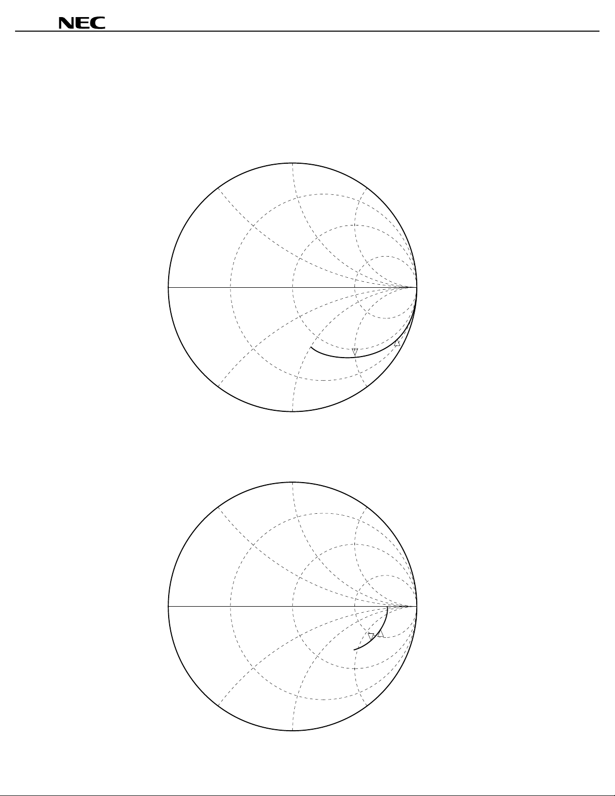
S-Parameter
VDS = 3 V, ID = 10 mA
START 100 MHz, STOP 3 GHz, STEP 100 MHz
NE76118
S11
1.0
0.5
0
–0.5
–1.0
S22
2.0
MARKERS
1: 1 GHz
2: 2 GHz
∞
2
1
–2.0
1.0
0.5
0
–0.5
–1.0
2.0
∞
2
1
–2.0
5
Page 6
NE76118
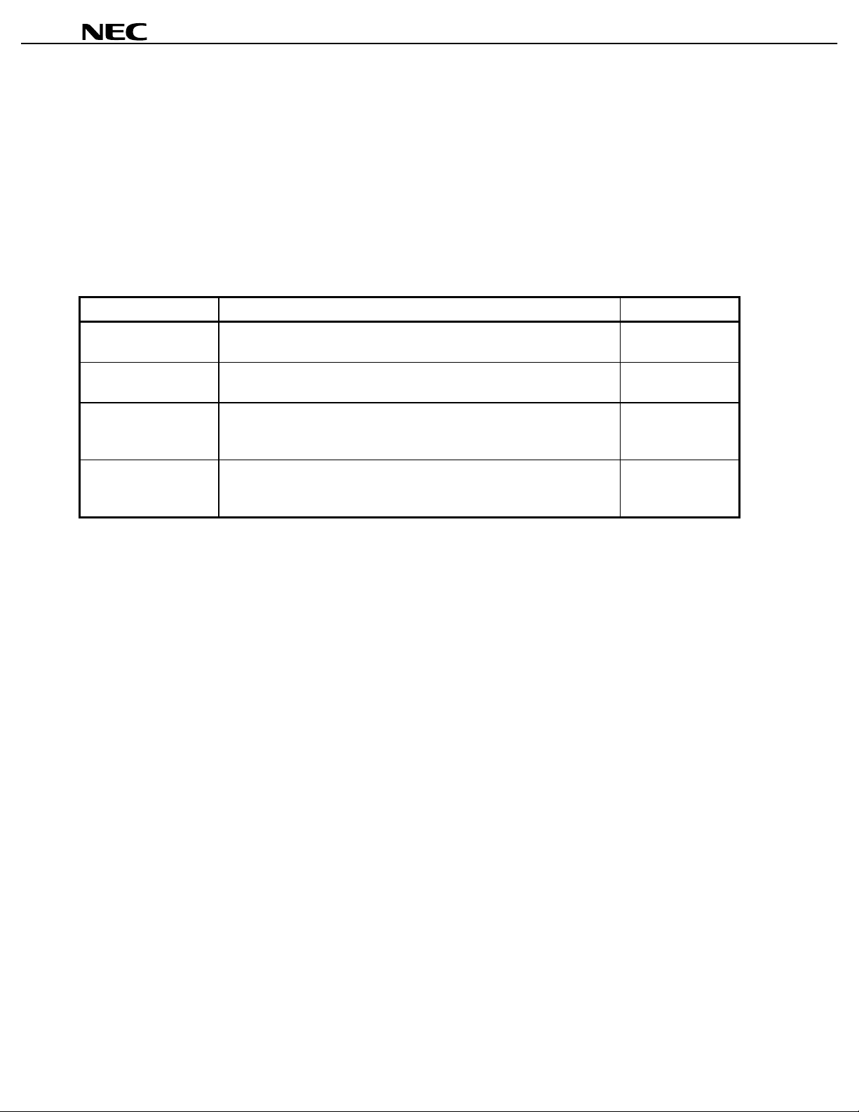
RECOMMENDED SOLDERING CONDITIONS
The following conditions (see table below) must be met when soldering this product.
Please consult with our sales offices in case other soldering process is used, or in case soldering is done under
different conditions.
<TYPES OF SURFACE MOUNT DEVICE>
For more details, refer to our document “SEMICONDUCTOR DEVICE MOUNTING TECHNOLOGY MANUAL”
(C10535E).
Soldering process Soldering conditions Symbol
VPS Package peak temperature : 215 °C, Time : 40 seconds MAX.
(200 °C MIN.), Number of times : 2, Number of days : not limited*
Wave soldering Soldering bath temperature : 260 °C MAX., Time : 10 seconds MAX.,
Number of times : 1, Number of days : not limited*
Infrared ray reflow Peak package’s surface temperature: 230 °C or below,
Reflow time: 30 seconds or below (210 °C or higher),
Number of reflow process: 2, Exposure limit*: None
Partial heating method Terminal temperature: 230 °C or below,
Flow time: 10 seconds or below,
Exposure limit*: None
VP15-00-2
WS60-00-1
IR30-00-2
* Exposure limit before soldering after dry-pack package is opened.
Storage conditions: 25 °C and relative humidity at 65 % or less.
Do not apply more than a single process at once, except for “Partial heating method”.
Note
PRECAUTION Avoid high static voltage and electric fields, because this device is MES FET with GaAs
shottky barrier gate.
6
Page 7

[MEMO]
NE76118
7
Page 8

NE76118
Caution
The Great Care must be taken in dealing with the devices in this guide.
The reason is that the material of the devices is GaAs (Gallium Arsenide), which is
designated as harmful substance according to the law concerned.
Keep the law concerned and so on, especially in case of removal.
No part of this document may be copied or reproduced in any form or by any means without the prior written
consent of NEC Corporation. NEC Corporation assumes no responsibility for any errors which may appear in this
document.
NEC Corporation does not assume any liability for infringement of patents, copyrights or other intellectual
property rights of third parties by or arising from use of a device described herein or any other liability arising
from use of such device. No license, either express, implied or otherwise, is granted under any patents,
copyrights or other intellectual property rights of NEC Corporation or others.
While NEC Corporation has been making continuous effort to enhance the reliability of its semiconductor devices,
the possibility of defects cannot be eliminated entirely. To minimize risks of damage or injury to persons or
property arising from a defect in an NEC semiconductor device, customers must incorporate sufficient safety
measures in its design, such as redundancy, fire-containment, and anti-failure features.
NEC devices are classified into the following three quality grades:
"Standard", "Special", and "Specific". The Specific quality grade applies only to devices developed based on
a customer designated "quality assurance program" for a specific application. The recommended applications
of a device depend on its quality grade, as indicated below. Customers must check the quality grade of each
device before using it in a particular application.
Standard: Computers, office equipment, communications equipment, test and measurement equipment,
audio and visual equipment, home electronic appliances, machine tools, personal electronic
equipment and industrial robots
Special: Transportation equipment (automobiles, trains, ships, etc.), traffic control systems, anti-disaster
systems, anti-crime systems, safety equipment and medical equipment (not specifically designed
for life support)
Specific: Aircrafts, aerospace equipment, submersible repeaters, nuclear reactor control systems, life
support systems or medical equipment for life support, etc.
The quality grade of NEC devices is "Standard" unless otherwise specified in NEC's Data Sheets or Data Books.
If customers intend to use NEC devices for applications other than those specified for Standard quality grade,
they should contact an NEC sales representative in advance.
Anti-radioactive design is not implemented in this product.
M4 96. 5
 Loading...