

Page 1

PRELIMINARY DATA SHEET
N-CHANNEL GaAs MES FET
NE650R279A
0.2 W L, S-BAND POWER GaAs MES FET
DESCRIPTION
The NE650R279A is a 0.2 W GaAs MES FET designed for middle power transmitter applications for mobile
communication handset and base station systems. It is capable of delivering 0.2 watt of output power (CW) with high
linear gain, high efficiency, excellent distortion and is suitable as a driver amplifier for our NE6500379A etc.
Reliability and performance uniformity are assured by NEC’s stringent quality and control procedures.
FEATURES
• High Output Power : P
• High Linear Gain : 16 dB typ.
• High Power Added Efficiency: 45% typ. @VDS = 6 V, I
O (1 dB)
= +23 dBm typ.
Dset
= 50 mA, f = 1.9 GHz
ORDERING INFORMATION (PLAN)
Part Number Package Supplying Form
NE650R279A-T1 79A 12 mm tape width, 1 kpcs / reel
Remark
To order evaluation samples, please contact your local NEC sales office.
(Part number for sample order: NE650R279A)
ABSOLUTE MAXIMUM RATINGS (TA = 25°C)
Operation in excess of any one of these parameters may result in permanent damage.
Parameter Symbol Ratings Unit
Drain to Source Voltage V
Gate to Source Voltage V
Drain Current I
Gate Forward Current I
Gate Reverse Current I
Total Power Dissipat i on P
Channel Temperature T
Storage Temperature T
DS
GSO
D
GF
GR
ch
stg
15 V
–7 V
0.3 A
8mA
8mA
T
2.1 W
150 °C
–65 to +150 °C
Caution Please handle this device at static-free workstation, because this is an electrostatic sensitive
device.
Document No. P13678EJ1V0DS00 (1st edition)
Date Published August 1998 N CP(K)
Printed in Japan
The information in this document is subject to change without notice.
1998©
Page 2

RECOMMENDED OPERATING LIMITS
Characteristics Symbol Test Conditions MIN. TYP. MAX. Unit
NE650R279A
Drain to Source Voltage V
DS
6.0 6.0 V
Gain Compression Gcomp 3.0 dB
Channel Temperature T
ch
+125 °C
ELECTRICAL CHARACTERISTICS
(TA = 25°C, Unless otherwise specified, using NEC standard test fixture.)
Characteristics Symbol Test Conditions MIN. TYP. MAX. Unit
BV
O (1 dB)
P
η
DSS
G
add
VDS = 2.5 V, VGS = 0 V 150 mA
p
VDS = 2.5 V, ID = 1 mA –2.5 –0.5 V
gd
Igd = 1 mA 13 V
th
Channel to Case 40 60 °C/W
f = 1.9 GHz, VDS = 6.0 V
g
= 30 Ω
R
Dset
= 50 mA (RF OFF)
D
I
Note 2
23.0 dBm
72 mA
45 %
L
15.0 16.0 dB
Saturated Drain Current I
Pinch-off Voltage V
Gate to Drain Break Down
Voltage
Thermal Resistance R
Output Power at 1 dB Gain
Compression Point
Drain Current I
Power Added Efficiency
Linear Gain
Note 1
Notes 1.
Pin = 0 dBm
DC performance is 100% testing. RF performance is testing several samples per wafer.
2.
Wafer rejection criteria for standard devices is 1 reject for several samples.
Preliminary Data Sheet2
Page 3

NE650R279A
NE650R279A S-PARAMETERS TEST CONDITIONS: VDS = 6.0 V, I
11
S
21
S
Dset
= 50 mA (Preliminary Data)
12
S
S
22
freq. (MHz) MAG. ANG. (deg.) MAG. ANG. (deg.) MAG. ANG. (deg.) MAG. ANG. (deg.)
1400 0.865 –103.4 5.788 133.2 0.070 53.2 0.403 –73.5
1500 0.861 –108.0 5.593 131.9 0.072 51.5 0.397 –76.7
1600 0.850 –112.1 5.439 130.8 0.073 51.1 0.392 –79.2
1700 0.839 –116.0 5.182 129.1 0.075 50.9 0.387 –82.1
1800 0.833 –120.5 5.026 129.1 0.078 50.6 0.382 –84.9
1900 0.827 –124.9 4.992 128.4 0.081 49.2 0.376 –87.5
2000 0.817 –129.4 4.888 125.6 0.082 47.2 0.368 –90.2
2100 0.809 –133.1 4.739 124.9 0.082 45.8 0.360 –93.0
2200 0.806 –137.7 4.628 123.6 0.081 45.6 0.349 –95.7
2300 0.795 –143.0 4.518 121.8 0.081 46.2 0.336 –98.5
2400 0.789 –148.3 4.403 119.9 0.083 46.5 0.325 –101.6
2500 0.781 –153.4 4.383 118.2 0.086 46.0 0.311 –104.9
2600 0.778 –157.5 4.348 116.6 0.087 44.3 0.300 –107.6
2700 0.779 –162.9 4.065 115.8 0.087 42.7 0.288 –110.5
2800 0.778 –167.0 3.910 113.8 0.085 42.2 0.276 –113.5
2900 0.778 –172.1 3.763 113.1 0.084 42.1 0.264 –117.3
3000 0.781 –176.7 3.632 112.8 0.083 41.4 0.256 –121.0
Preliminary Data Sheet 3
Page 4
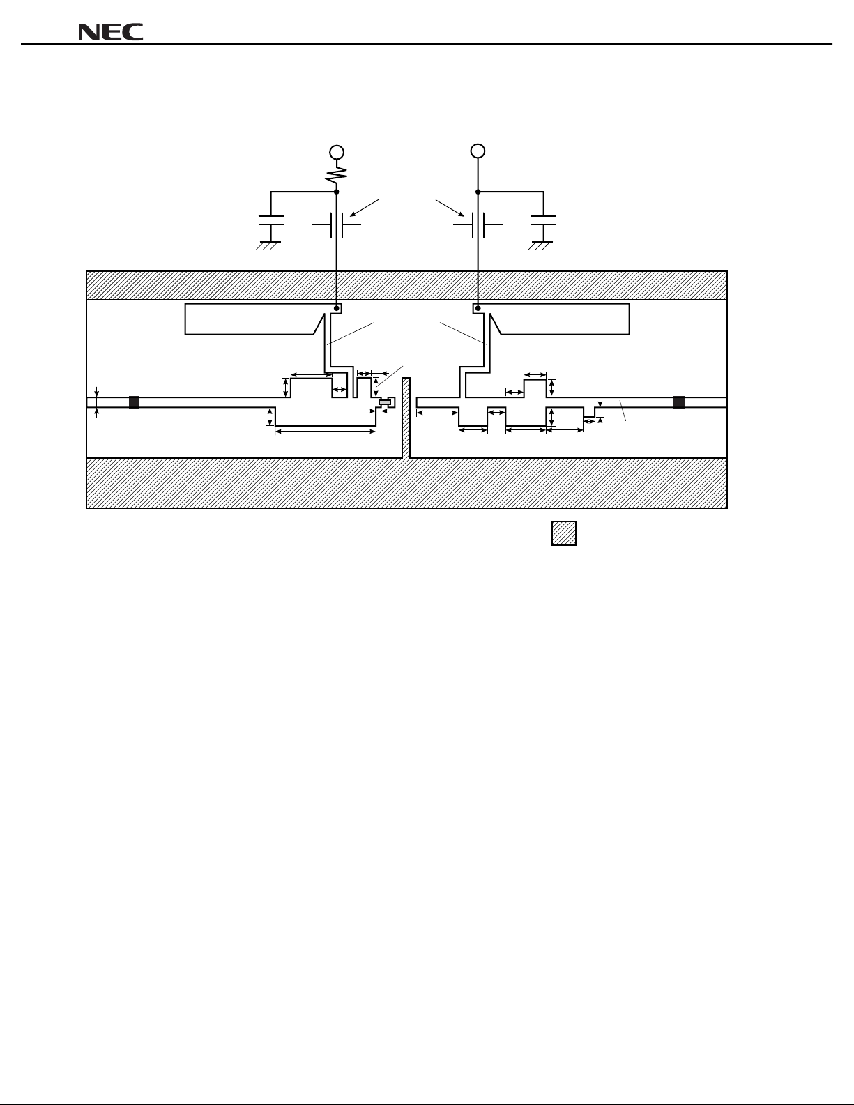
APPLICATION CIRCUIT EXAMPLE (Unit: mm)
VGS VDS
Rg
NE650R279A
2
INPUT
Tantalum Condenser
C1
µ
47 F
/4 OPEN STUB
λ
5
4
f = 1.9 GH
VDS = 6 V
Dset
I
Z
= 50 mA (RF OFF)
1000 p
λ
/4 LINE
9
21
32
3
C1 = 30 pF
C2 = 30 pF
4
R1
1
10
7.5 87
R1 = 5.1 Ω
Rg = 30 Ω
λ
4
4
Tantalum Condenser
µ
100 F
/4 OPEN STUB
5
3
4
Substrate: Teflon glass ( r = 2.6)
t = 0.8 mm
2
2
GND
50 Ω LINE
C2
OUTPUT
ε
Preliminary Data Sheet4
Page 5
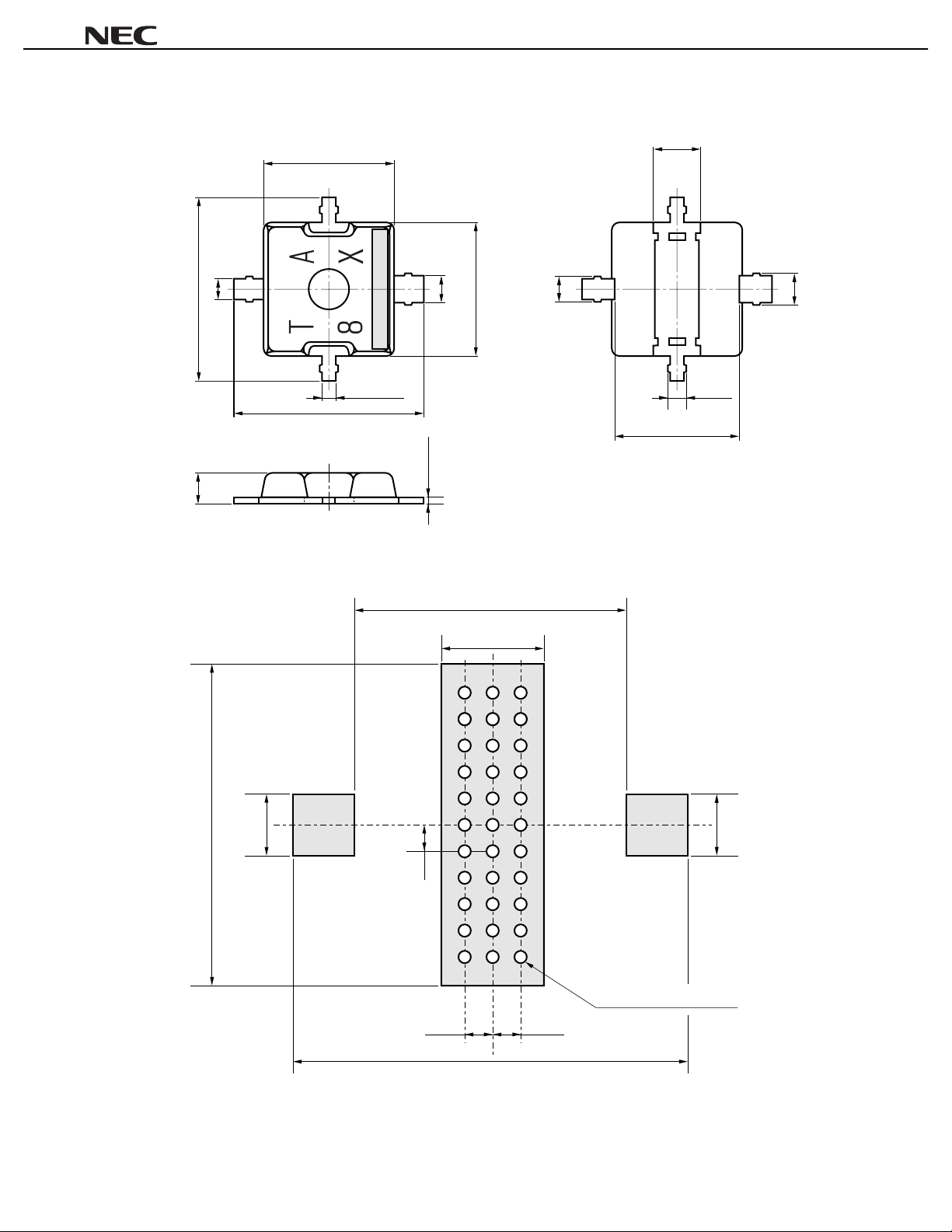
79A Package Dimensions (Unit: mm)
NE650R279A
4.2 max.
Source
Gate Gate
5.7 max.
0.6 ±0.15
0.4 ±0.15
5.7 max.
0.9 ±0.2
Drain Drain
4.4 max.
0.8 ±0.15
0.2 ±0.1
79A Package Recommended P.C.B. Layout (Unit: mm)
1.0 max.
1.5 ±0.2
Source
1.2 max.
0.8 max.
3.6 ±0.2
Bottom View
5.9
1.2
4.0
1.7
Stop up the hole with a rosin
or something to avoid solder
flow.
Drain Gate
0.5
Source
through hole 0.2 × 33
0.5 0.5
1.0
φ
6.1
Preliminary Data Sheet 5
Page 6
NE650R279A
RECOMMENDED SOLDERING CONDITIONS
This product should be soldered under the following recommended conditions. For soldering methods and
conditions other than those recommended below, contact your NEC sales representative.
Soldering Method Soldering Conditions
Infrared Reflow Package peak temperature: 235°C or below
Time: 30 seconds or less (at 210°C)
Count: 2, Exposure limi t
Partial Heating Pin temperature: 260°C
Time: 5 seconds or less (per pi n row)
Exposure limit
After opening the dry pack, keep it in a place below 25°C and 65% RH for the allowable storage period.
Note
Note
: None
Note
: None
Caution Do not use different soldering methods together (except for partial heating).
Recommended
Condition Symbol
IR35-00-2
–
Preliminary Data Sheet6
Page 7
[MEMO]
NE650R279A
Preliminary Data Sheet 7
Page 8
NE650R279A
Caution
The Great Care must be taken in dealing with the devices in this guide.
The reason is that the material of the devices is GaAs (Gallium Arsenide), which is
designated as harmful substance according to the law concerned.
Keep the law concerned and so on, especially in case of removal.
The application circuits and their parameters are for reference only and are not intended for use in actual design-ins.
No part of this document may be copied or reproduced in any form or by any means without the prior written
consent of NEC Corporation. NEC Corporation assumes no responsibility for any errors which may appear in this
document.
NEC Corporation does not assume any liability for infringement of patents, copyrights or other intellectual
property rights of third parties by or arising from use of a device described herein or any other liability arising
from use of such device. No license, either express, implied or otherwise, is granted under any patents,
copyrights or other intellectual property rights of NEC Corporation or others.
While NEC Corporation has been making continuous effort to enhance the reliability of its semiconductor devices,
the possibility of defects cannot be eliminated entirely. To minimize risks of damage or injury to persons or
property arising from a defect in an NEC semiconductor device, customers must incorporate sufficient safety
measures in its design, such as redundancy, fire-containment, and anti-failure features.
NEC devices are classified into the following three quality grades:
"Standard", "Special", and "Specific". The Specific quality grade applies only to devices developed based on
a customer designated "quality assurance program" for a specific application. The recommended applications
of a device depend on its quality grade, as indicated below. Customers must check the quality grade of each
device before using it in a particular application.
Standard: Computers, office equipment, communications equipment, test and measurement equipment,
audio and visual equipment, home electronic appliances, machine tools, personal electronic
equipment and industrial robots
Special: Transportation equipment (automobiles, trains, ships, etc.), traffic control systems, anti-disaster
systems, anti-crime systems, safety equipment and medical equipment (not specifically designed
for life support)
Specific: Aircrafts, aerospace equipment, submersible repeaters, nuclear reactor control systems, life
support systems or medical equipment for life support, etc.
The quality grade of NEC devices is "Standard" unless otherwise specified in NEC's Data Sheets or Data Books.
If customers intend to use NEC devices for applications other than those specified for Standard quality grade,
they should contact an NEC sales representative in advance.
Anti-radioactive design is not implemented in this product.
M4 96. 5
 Loading...