

Page 1
Philips Semiconductors Product specification
NE/SA612ADouble-balanced mixer and oscillator
1
1990 Sep 17 853-0391 00446
DESCRIPTION
The NE/SA612A is a low-power VHF monolithic double-balanced
mixer with on-board oscillator and voltage regulator. It is intended for
low cost, low power communication systems with signal frequencies
to 500MHz and local oscillator frequencies as high as 200MHz. The
mixer is a “Gilbert cell” multiplier configuration which provides gain
of 14dB or more at 45MHz.
The oscillator can be configured for a crystal, a tuned tank
operation, or as a buffer for an external L.O. Noise figure at 45MHz
is typically below 6dB and makes the device well suited for high
performance cordless phone/cellular radio. The low power
consumption makes the NE/SA612A excellent for battery operated
equipment. Networking and other communications products can
benefit from very low radiated energy levels within systems. The
NE/SA612A is available in an 8-lead dual in-line plastic package and
an 8-lead SO (surface mounted miniature package).
FEATURES
•Low current consumption
•Low cost
•Operation to 500MHz
•Low radiated energy
•Low external parts count; suitable for crystal/ceramic filter
•Excellent sensitivity, gain, and noise figure
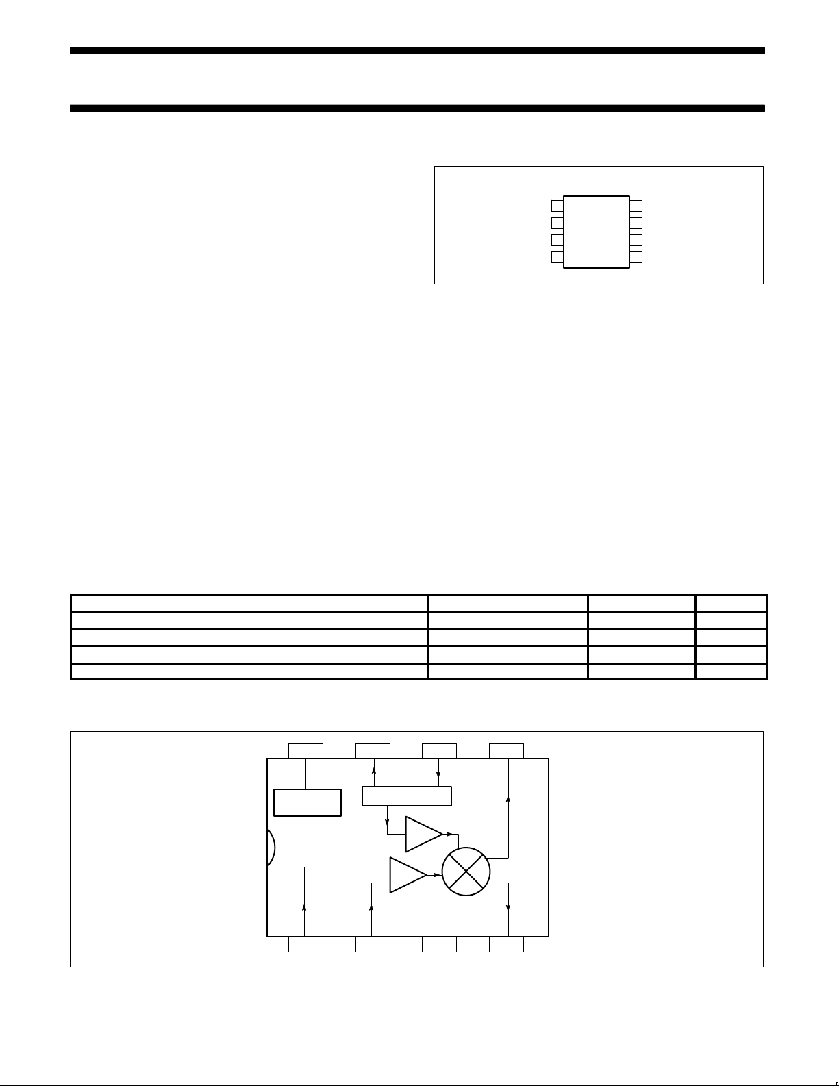
PIN CONFIGURATION
D, N Packages
8
7
6
5
1
2
3
4
INPUT A
INPUT B
GND
OUTPUT A
OSCILLATOR
OSCILLATOR
OUTPUT B
V
CC
SR00098
Figure 1. Pin Configuration
APPLICATIONS
•Cordless telephone
•Portable radio
•VHF transceivers
•RF data links
•Sonabuoys
•Communications receivers
•Broadband LANs
•HF and VHF frequency conversion
•Cellular radio mixer/oscillator
ORDERING INFORMATION
DESCRIPTION TEMPERATURE RANGE ORDER CODE DWG #
8-Pin Plastic Dual In-Line Plastic (DIP) 0 to +70°C NE612AN SOT97-1
8-Pin Plastic Small Outline (SO) package (Surface-Mount) 0 to +70°C NE612AD SOT96-1
8-Pin Plastic Dual In-Line Plastic (DIP) -40 to +85°C SA612AN SOT97-1
8-Pin Plastic Small Outline (SO) package (Surface-Mount) -40 to +85°C SA612AD SOT96-1
BLOCK DIAGRAM
8 7 6 5
4321
OSCILLATOR
VOLTAGE
REGULATOR
GROUND
V
CC
SR00099
Figure 2. Block Diagram
Page 2
Philips Semiconductors Product specification
NE/SA612ADouble-balanced mixer and oscillator
1990 Sep 17
2
ABSOLUTE MAXIMUM RATINGS
SYMBOL PARAMETER RATING UNIT
V
CC
Maximum operating voltage 9 V
T
STG
Storage temperature -65 to +150 °C
T
A
Operating ambient temperature range
NE
SA
0 to +70
-40 to +85
°C
AC/DC ELECTRICAL CHARACTERISTICS
TA=25°C, V
CC
= 6V, Figure 3
LIMITS
SYMBOL
PARAMETER
TEST CONDITION
Min Typ Max
UNIT
V
CC
Power supply voltage range 4.5 8.0 V
DC current drain 2.4 3.0 mA
f
IN
Input signal frequency 500 MHz
f
OSC
Oscillator frequency 200 MHz
Noise figured at 45MHz 5.0 dB
Third-order intercept point at 45MHz RFIN=-45dBm -13 dBm
Conversion gain at 45MHz 14 17 dB
R
IN
RF input resistance 1.5 kΩ
C
IN
RF input capacitance 3 pF
Mixer output resistance (Pin 4 or 5) 1.5 kΩ
DESCRIPTION OF OPERATION
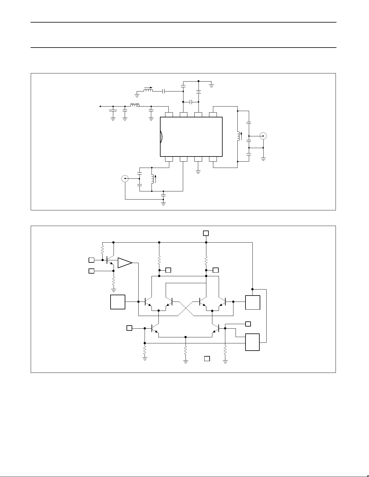
The NE/SA612A is a Gilbert cell, an oscillator/buffer, and a
temperature compensated bias network as shown in the equivalent
circuit. The Gilbert cell is a differential amplifier (Pins 1 and 2) which
drives a balanced switching cell. The differential input stage
provides gain and determines the noise figure and signal handling
performance of the system.
The NE/SA612A is designed for optimum low power performance.
When used with the NE614A as a 45MHz cordless phone/cellular
radio 2nd IF and demodulator, the NE/SA612A is capable of
receiving -119dBm signals with a 12dB S/N ratio. Third-order
intercept is typically -15dBm (that’s approximately +5dBm output
intercept because of the RF gain). The system designer must be
cognizant of this large signal limitation. When designing LANs or
other closed systems where transmission levels are high, and
small-signal or signal-to-noise issues not critical, the input to the
NE/SA612A should be appropriately scaled.
Page 3
Philips Semiconductors Product specification
NE/SA612ADouble-balanced mixer and oscillator
1990 Sep 17
3
TEST CONFIGURATION
8 7 6 5
4321
OUTPUT
150pF
330pF
120pF
1.5 to
100nF
220pF
INPUT
47pF
22pF
1nF
100nF
10nF
V
CC
6.8µF
5.5µH
0.209 to
0.283µH
44.2µH
10pF
34.545MHz THIRD OVERTONE CRYSTAL
612A
0.5 to 1.3µH
SR00101
Figure 3. Test Configuration
1
2
3
4 5
6
7
8
GND
BUFFER
1.5k
BIAS
BIAS
BIAS
1.5k
1.5k
1.5k
V
CC
18k
25k
SR00102
Figure 4. Equivalent Circuit
Page 4
Philips Semiconductors Product specification
NE/SA612ADouble-balanced mixer and oscillator
1990 Sep 17
4
Besides excellent low power performance well into VHF, the
NE/SA612A is designed to be flexible. The input, output, and
oscillator ports can support a variety of configurations provided the
designer understands certain constraints, which will be explained
here.
The RF inputs (Pins 1 and 2) are biased internally. They are
symmetrical. The equivalent AC input impedance is approximately
1.5k || 3pF through 50MHz. Pins 1 and 2 can be used
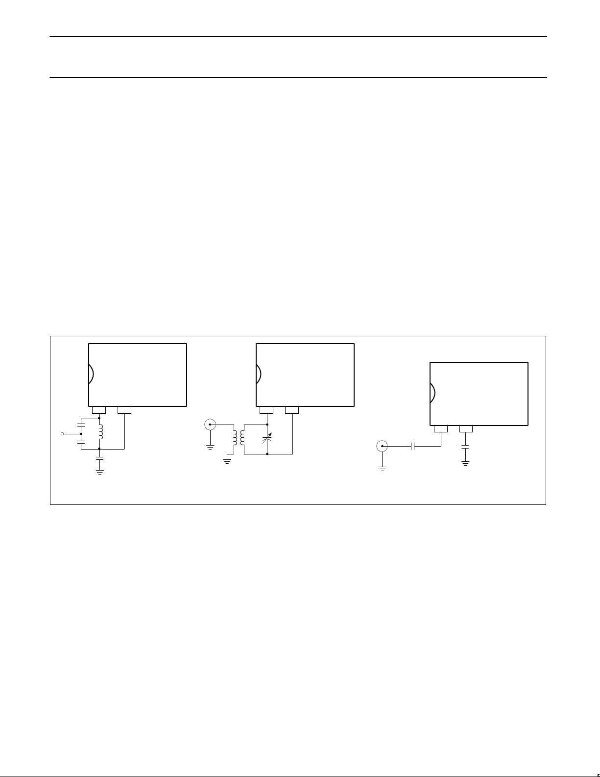
interchangeably, but they should not be DC biased externally. Figure
5 shows three typical input configurations.
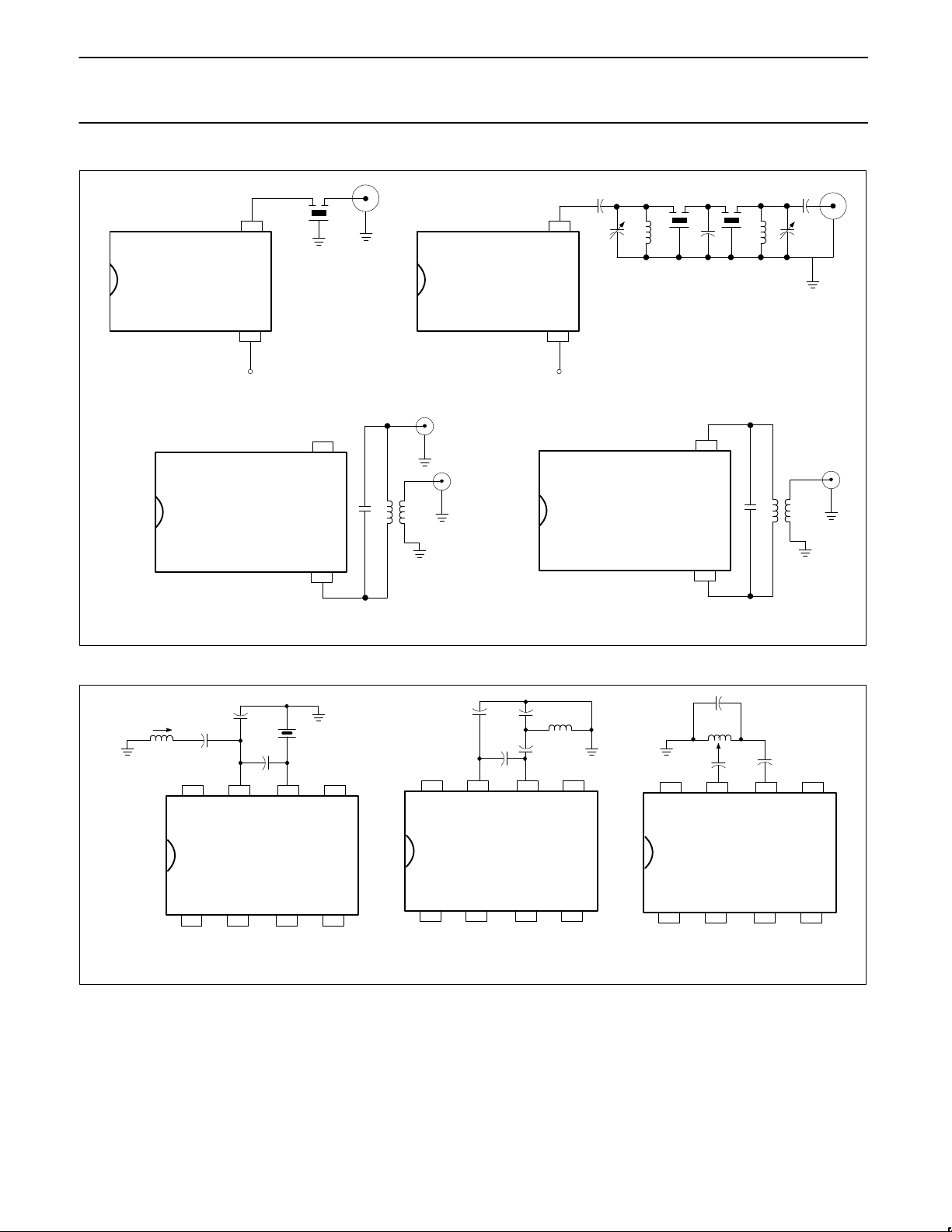
The mixer outputs (Pins 4 and 5) are also internally biased. Each
output is connected to the internal positive supply by a 1.5kΩ
resistor. This permits direct output termination yet allows for
balanced output as well. Figure 6 shows three single-ended output
configurations and a balanced output.
The oscillator is capable of sustaining oscillation beyond 200MHz in
crystal or tuned tank configurations. The upper limit of operation is
determined by tank “Q” and required drive levels. The higher the Q
of the tank or the smaller the required drive, the higher the
permissible oscillation frequency. If the required L.O. is beyond
oscillation limits, or the system calls for an external L.O., the
external signal can be injected at Pin 6 through a DC blocking
capacitor. External L.O. should be 200mV
P-P
minimum to 300mV
P-P
maximum.
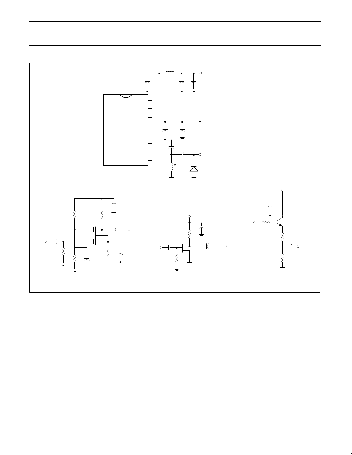
Figure 7 shows several proven oscillator circuits. Figure 7a is
appropriate for cordless phones/cellular radio. In this circuit a third
overtone parallel-mode crystal with approximately 5pF load
capacitance should be specified. Capacitor C3 and inductor L1 act
as a fundamental trap. In fundamental mode oscillation the trap is
omitted.
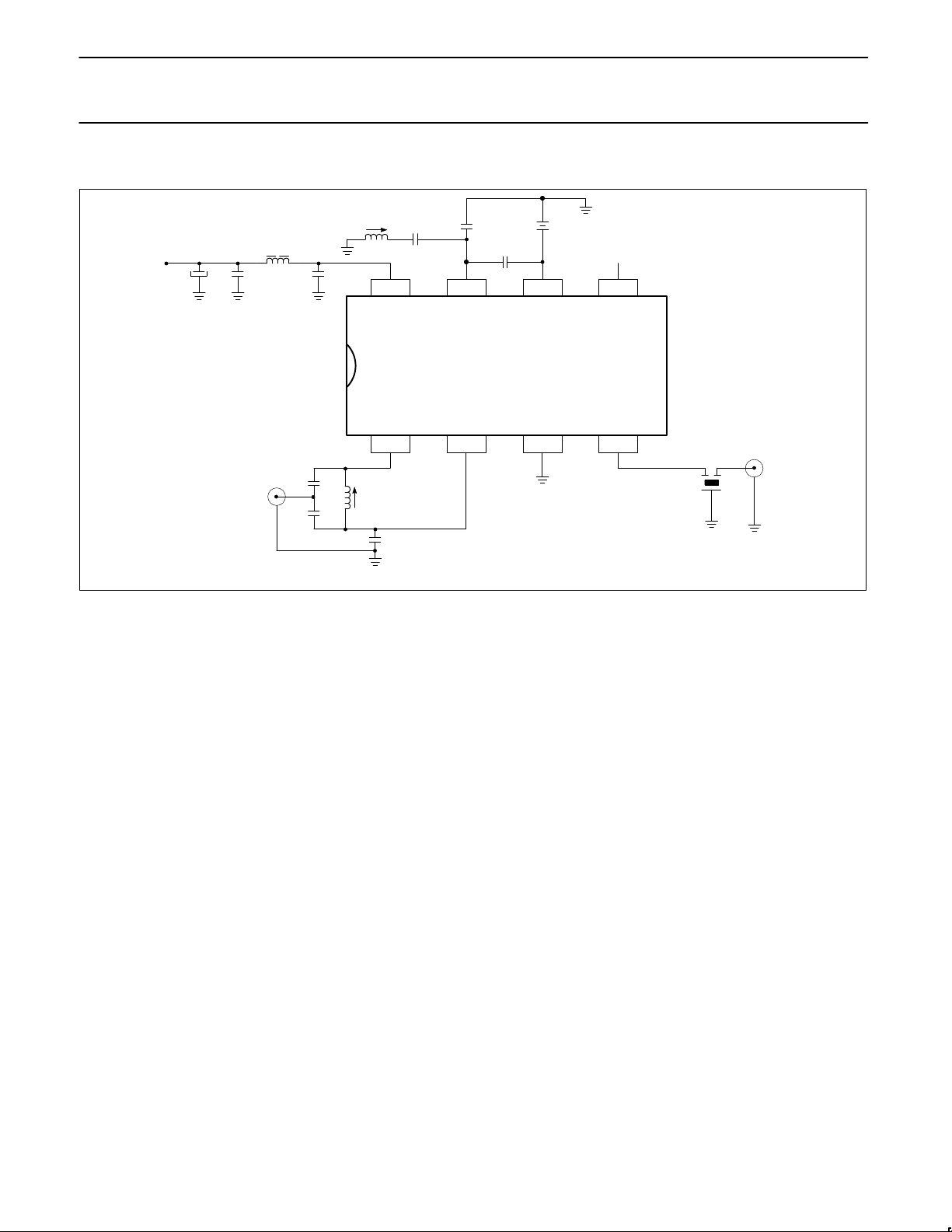
Figure 8 shows a Colpitts varacter tuned tank oscillator suitable for
synthesizer-controlled applications. It is important to buffer the
output of this circuit to assure that switching spikes from the first
counter or prescaler do not end up in the oscillator spectrum. The
dual-gate MOSFET provides optimum isolation with low current.
The FET offers good isolation, simplicity, and low current, while the
bipolar circuits provide the simple solution for non-critical
applications. The resistive divider in the emitter-follower circuit
should be chosen to provide the minimum input signal which will
assume correct system operation.
INPUT
612A
1 2
612A
1 2
612A
1 2
a. Single-Ended Tuned Input b. Balanced Input (For Attenuation
of Second-Order Products)
c. Single-Ended Untuned Input
SR00103
Figure 5. Input Configuration
Page 5
Philips Semiconductors Product specification
NE/SA612ADouble-balanced mixer and oscillator
1990 Sep 17
5
612A
4
5
612A
4
5
612A
4
5
612A
4
5
a. Single-Ended Ceramic Filter b. Single-Ended Crystal Filter
c. Single-Ended IFT d.. Balanced Output
CFU455
or Equivalent
12pF
C
T
*
*C
T
matches 3.5kΩ to next stage
Filter K&L 38780 or Equivalent
SR00104
Figure 6. Output Configuration
612A
4
5
a. Colpitts Crystal Oscillator
(Overtone Mode)
b. Colpitts L/C Tank Oscillator
c. Hartley L/C Tank Oscillator
3
6
2
7
1
8
612A
4
5
3
6
2
7
1
8
612A
4
5
3
6
2
7
1
8
TC02101S TC02111S TC02121S
XTAL
L
1
C
1
C
2
C
3
SR00105
Figure 7. Oscillator Circuits
Page 6
Philips Semiconductors Product specification
NE/SA612ADouble-balanced mixer and oscillator
1990 Sep 17
6
612A
4
5
3
6
2
7
1
8
+6V
7pF
10pF
TO
BUFFER
DC CONTROL VOLTAGE
FROM SYNTHESIZER
MV2105
OR EQUIVALENT
1000pF
1000pF
5.5µH
0.10pF
10µF
0.06µH
0.1µF
3SK126
100k
2pF
TO SYNTHESIZER
100k
100k
330
2k
TO SYNTHESIZER
2N5484
2N918
0.01µF
0.01µF
1.0nF
0.01pF
SR00106
Figure 8. Colpitts Oscillator Suitable for Synthesizer Applications and Typical Buffers
Page 7
Philips Semiconductors Product specification
NE/SA612ADouble-balanced mixer and oscillator
1990 Sep 17
7
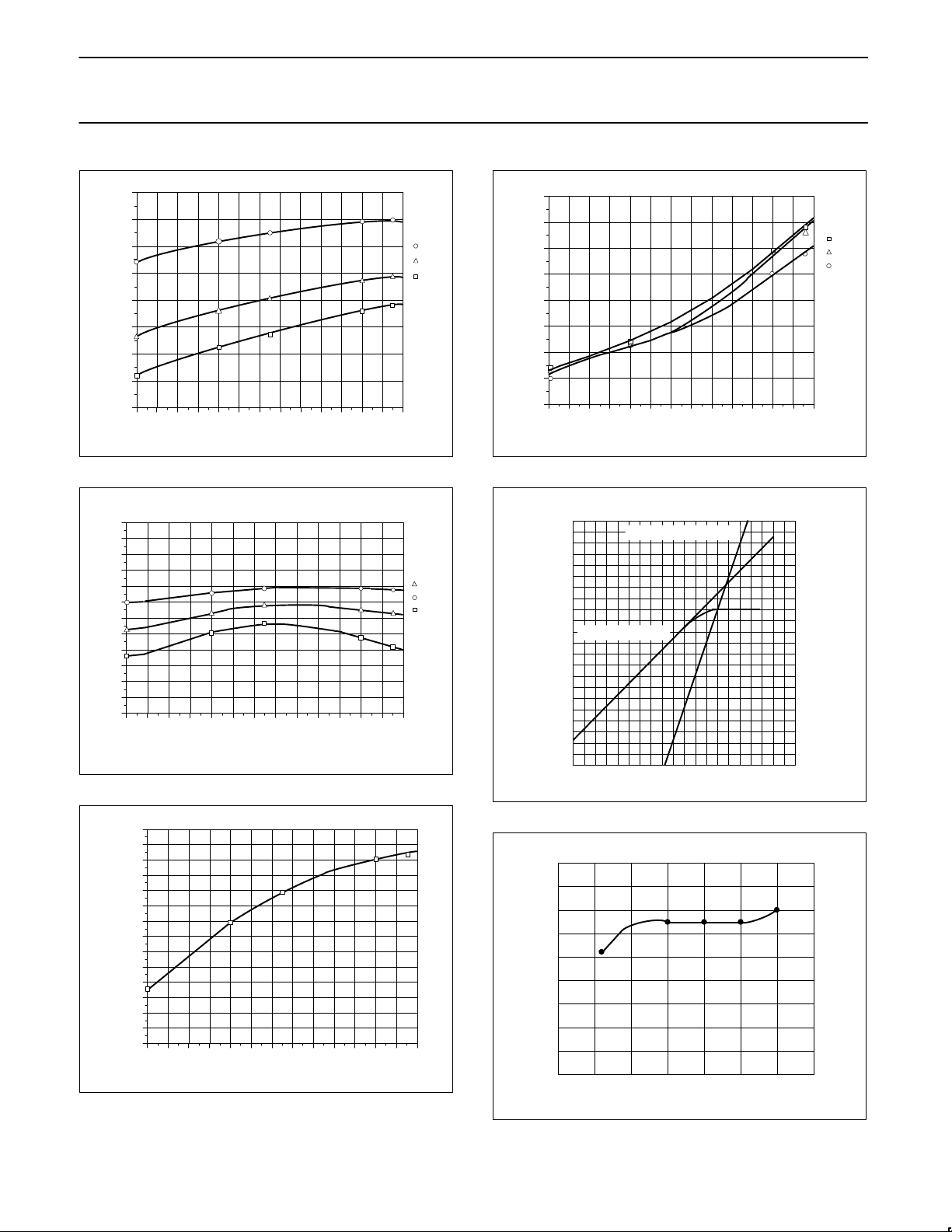
TEST CONFIGURATION
8 7 6 5
4321
SFG455A3
100nF
220pF
INPUT
47pF
22pF
1nF
100nF
10nF
V
CC
6.8µF
0.5 to 1.3µH
0.209 to 0.283µH
5.6pF
44.545MHz THIRD OVERTONE CRYSTAL
612A
OR EQUIVALENT
455kHZ
45MHz IN
5.5µH
SR00107
Figure 9. Typical Application for Cordless/Cellular Radio
Page 8
Philips Semiconductors Product specification
NE/SA612ADouble-balanced mixer and oscillator
1990 Sep 17
8
3.50
3.25
3.00
2.75
2.50
2.25
2.00
1.75
1.50
–40 –30 –20 –10 0 10 20 30 40 50 60 70 80 90
SUPPLY CURRENT 9mA)
TEMPERATURE OC
4.5V
6.0V
8.5V
SR00108
Figure 10. ICC vs Supply Voltage
–40 –30 –20 –10 0 10 20 30 40 50 60 70 80 90
20.0
19.5
19.0
18.5
18.0
17.5
17.0
16.5
16.0
15.5
15.0
14.5
14.0
CONVERSION GAIN (dB)
TEMPERATURE OC
4.5V
6.0V
8.5V
SR00109
Figure 11. Conversion Gain vs Supply Voltage
–10.0
–10.5
–11.0
–11.5
–12.0
–12.5
–13.0
–13.5
–14.0
INPUT INTERCEPT POINT (dBm)
–14.5
–15.0
–15.5
–16.0
–16.5
–17.0
TEMPERATURE
O
C
–40 –30 –20 –10 0 10 20 30 40 50 60 70 80 90
SR00110
Figure 12. Third-Order Intercept Point
6.00
5.75
5.50
5.25
5.00
4.75
4.50
4.25
4.00
–40 –30 –20 –10 0 10 20 30 40 50 60 70 80 90
NOISE FIGURE (dB)
TEMPERATURE OC
4.5V
6.0V
8.5V
SR00111
Figure 13. Noise Figure
–80 –60 –40 –20 0 20
20
0
–20
–40
–60
3rd ORDER PRODUCT
FUND. PRODUCT
IF OUTPUT POWER (dBm)
RF INPUT LEVEL (dBm)
RF
1
= 45MHz, IF = 455kHz, RF2 = 45.06MHz
SR00112
Figure 14. Third-Order Intercept and Compression
–10
–11
–12
–13
–14
–15
–16
–17
–18
4 5 6 7 8 9 10
VCC (VOLTS)
INTERCEPT (dBm)
SR00113
Figure 15. Input Third-Order Intermod Point vs V
CC
 Loading...