

Page 1

INTEGRATED CIRCUITS
NE/SA572
Programmable analog compandor
Product specification 1987 Oct 7
IC17 Data Handbook
Page 2

Philips Semiconductors Product specification
NE/SA572Programmable analog compandor
DESCRIPTION
The NE572 is a dual-channel, high-performance gain control circuit
in which either channel may be used for dynamic range
compression or expansion. Each channel has a full-wave rectifier to
detect the average value of input signal, a linearized,
temperature-compensated variable gain cell (∆G) and a dynamic
time constant buffer. The buf fer permits independent control of
dynamic attack and recovery time with minimum external
components and improved low frequency gain control ripple
distortion over previous compandors.
The NE572 is intended for noise reduction in high-performance
audio systems. It can also be used in a wide range of
communication systems and video recording applications.
FEA TURES
•Independent control of attack and recovery time
•Improved low frequency gain control ripple
•Complementary gain compression and expansion with external op
amp
•Wide dynamic range—greater than 110dB
•T emperature-compensated gain control
•Low distortion gain cell
•Low noise—6µV typical
•Wide supply voltage range—6V-22V
•System level adjustable with external components
PIN CONFIGURATION
D1, N, F Packages
TRACK TRIM A
RECOV. CAP A
RECT. IN A
ATTACK CAP A
∆G OUT A
THD TRIM A
NOTE:
1. D package released in large SO (SOL) package only.
1
2
3
4
5
6
∆G IN A
7
8
GND
Figure 1. Pin Configuration
APPLICATIONS
•Dynamic noise reduction system
•Voltage control amplifier
•Stereo expandor
•Automatic level control
•High-level limiter
•Low-level noise gate
•State variable filter
16
V
CC
15
TRACK TRIM B
14
RECOV. CAP B
13
RECT. IN B
12
ATTACK CAP B
∆G OUT B
11
10
THD TRIM B
∆G IN B
9
SR00694
ORDERING INFORMATION
DESCRIPTION TEMPERATURE RANGE ORDER CODE DWG #
16-Pin Plastic Small Outline (SO) 0 to +70°C NE572D SOT109-1
16-Pin Plastic Dual In-Line Package (DIP) 0 to +70°C NE572N SOT38-4
16-Pin Plastic Small Outline (SO) –40 to +85°C SA572D SOT109-1
16-Pin Ceramic Dual In-Line Package (Cerdip) –40 to +85°C SA572F 0582B
16-Pin Plastic Dual In-Line Package (DIP) –40 to +85°C SA572N SOT38-4
ABSOLUTE MAXIMUM RATINGS
SYMBOL PARAMETER RATING UNIT
V
CC
T
A
P
D
Supply voltage 22 V
Operating temperature range
NE572 0 to +70 °C
SA572 –40 to +85
Power dissipation 500 mW
DC
1987 Oct 7 853-0813 90829
2
Page 3

Philips Semiconductors Product specification
SYMBOL
PARAMETER
TEST CONDITIONS
UNIT
NE/SA572Programmable analog compandor
BLOCK DIAGRAM
(7,9)
(6,10)
(3,13)
(16)
R1
6.8k
∆G
500
Ω
GAIN CELL
–
+
270
Ω
RECTIFIER
P.S.
(8) (4,12) (2,14)
10k
–
+
BUFFER 10k
(5,11)
(1,15)
SR00695
Figure 2. Block Diagram
DC ELECTRICAL CHARACTERISTICS
Standard test conditions (unless otherwise noted) VCC=15V, TA=25°C; Expandor mode (see Test Circuit). Input signals at unity gain level (0dB)
= 100mV
V
CC
I
CC
V
R
THD
THD
THD
PSRR
at 1kHz; V
RMS
1
Supply voltage 6 22 6 22 V
Supply current No signal 6 6.3 mA
Internal voltage reference 2.3 2.5 2.7 2.3 2.5 2.7 V
Total harmonic distortion
(untrimmed)
Total harmonic distortion
(trimmed)
Total harmonic distortion
(trimmed)
No signal output noise
DC level shift (untrimmed)
Unity gain level –1 0 +1 –1.5 0 +1.5 dB
Large–signal distortion V1=V2=400mV 0.7 3.0 0.7 3 %
Tracking error (measured
relative to value at unity Rectifier input
gain)= V2=+6dB V1=0dB ±0.2 ±0.2
[VO–VO (unity gain)]dB V2=–30dB V1=0dB ±0.5 –1.5 ±0.5 –2.5 dB
–V2dB +0.8 +1.6
Channel crosstalk
Power supply rejection ra-
tio
= V2; R
= 3.3kΩ; R
2
= 17.3kΩ.
3
1kHz CA=1.0µF 0.2 1.0 0.2 1.0 %
1kHz CR=10µF 0.05 0.05 %
100Hz 0.25 0.25 %
Input to V1 and V2 grounded
(20–20kHz)
Input change from no signal to
100mV
RMS
200mV
into channel A, measured
RMS
output on channel B
120Hz 70 70 dB
NE572 SA572
Min Typ Max Min Typ Max
DC
DC
6 25 6 25 µV
±20 ±50 ±20 ±50 mV
60 60 dB
1987 Oct 7
3
Page 4

Philips Semiconductors Product specification
NE/SA572Programmable analog compandor
TEST CIRCUIT
2.2µF
V
1
5Ω
= 10µF
2.2µF
1%
R
2
3.3k (3,13)
V
2
(7,9)
6.8k
(2,14)
(4,12)
∆G
BUFFER
RECTIFIER
(5,11)
(6,10)
(8)
(1,15)
(16)
Figure 3. Test Circuit
AUDIO SIGNAL PROCESSING IC COMBINES VCA
AND FAST ATTACK/SLOW RECOVERY LEVEL
SENSOR
In high-performance audio gain control applications, it is desirable to
independently control the attack and recovery time of the gain
control signal. This is true, for example, in compandor applications
for noise reduction. In high end systems the input signal is usually
split into two or more frequency bands to optimize the dynamic
behavior for each band. This reduces low frequency distortion due
to control signal ripple, phase distortion, high frequency channel
overload and noise modulation. Because of the expense in
hardware, multiple band signal processing up to now was limited to
professional audio applications.
With the introduction of the Signetics NE572 this high-performance
noise reduction concept becomes feasible for consumer hi fi
applications. The NE572 is a dual channel gain control IC. Each
channel has a linearized, temperature-compensated gain cell and an
improved level sensor. In conjunction with an external low noise op
amp for current-to-voltage conversion, the VCA features low
distortion, low noise and wide dynamic range.
The novel level sensor which provides gain control current for the
VCA gives lower gain control ripple and independent control of fast
attack, slow recovery dynamic response. An attack capacitor C
with an internal 10k resistor RA defines the attack time tA. The
recovery time t
C
and an internal 10k resistor RR. Typical attack time of 4ms for
R
of a tone burst is defined by a recovery capacitor
R
the high-frequency spectrum and 40ms for the low frequency band
can be obtained with 0.1µF and 1.0µF attack capacitors,
respectively. Recovery time of 200ms can be obtained with a 4.7µF
recovery capacitor for a 100Hz signal, the third harmonic distortion
is improved by more than 10dB over the simple RC ripple filter with
a single 1.0µF attack and recovery capacitor, while the attack time
remains the same.
A
+
22µF
22µF
100Ω
V
+15V
–15V
0
82k
1k +
2.2k
2.2µF
1%
R
17.3k
270pF
1µF
3
–
NE5234
+
.1µF
+
The NE572 is assembled in a standard 16-pin dual in-line plastic
package and in oversized SOL package. It operates over a wide
supply range from 6V to 22V . Supply current is less than 6mA. The
NE572 is designed for consumer application over a temperature
range 0-70
The SA572 is intended for applications from –40°C to
+85°C.
NE572 BASIC APPLICATIONS
Description
The NE572 consists of two linearized, temperature-compensated
gain cells (∆G), each with a full-wave rectifier and a buffer amplifier
as shown in the block diagram. The two channels share a 2.5V
common bias reference derived from the power supply but
otherwise operate independently. Because of inherent low distortion,
low noise and the capability to linearize large signals, a wide
dynamic range can be obtained. The buffer amplifiers are provided
to permit control of attack time and recovery time independent of
each other. Partitioned as shown in the block diagram, the IC allows
flexibility in the design of system levels that optimize DC shift, ripple
distortion, tracking accuracy and noise floor for a wide range of
application requirements.
Gain Cell
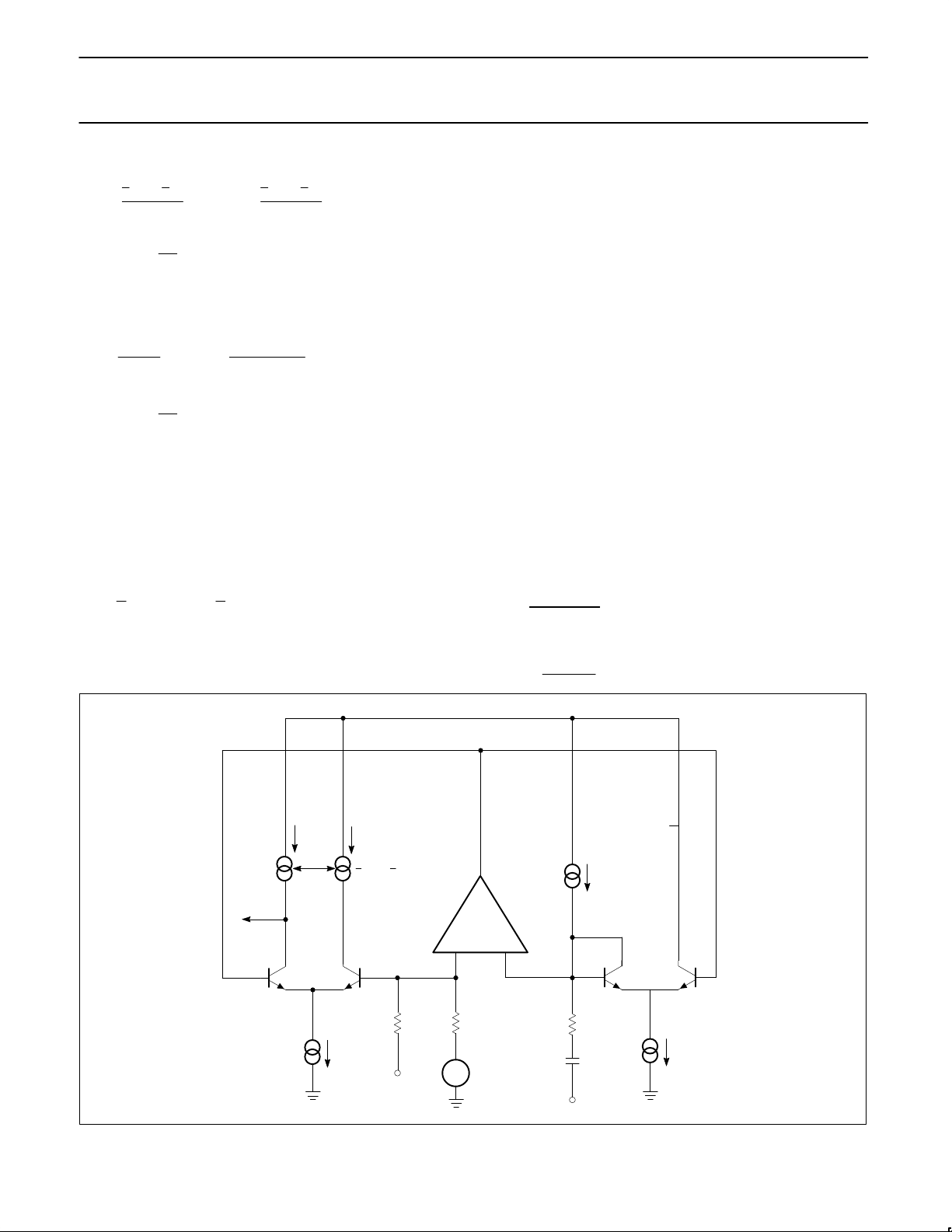
Figure 4 shows the circuit configuration of the gain cell. Bases of the
differential pairs Q
inputs of OPA A
of Q1-Q2 and the VBE of Q3-Q4 equal. The following relationship can
be derived from the transistor model equation in the forward active
region.
V
BE
Q3Q4
(VBE = VT IIN IC/IS)
and Q3-Q4 are both tied to the output and
1-Q2
. The negative feedback through Q1 holds the V
1
BE
Q1Q2
SR00696
BE
1987 Oct 7
4
Page 5
Philips Semiconductors Product specification
NE/SA572Programmable analog compandor
I
V
ǒ
n
T
where I
1
1
I
)
I
G
2
IN
O
2
* VTI
Ǔ
I
S
V
IN
+
R
1
1
1
I
*
I
G
2
ǒ
n
O
2
Ǔ
I
S
R1 = 6.8kΩ
= 140µA
I
1
I
= 280µA
2
ǒ
I
V
n
T
where I
I1) I
I
IN
IN
Ǔ
* VTI
S
V
IN
+
R
1
I2* I1* I
ǒ
n
IN
Ǔ
I
S
(2)
R1 = 6.8kΩ
= 140µA
I
1
I
= 280µA
2
I
is the differential output current of the gain cell and IG is the gain
O
control current of the gain cell.
If all transistors Q
through Q4 are of the same size, equation (2)
1
can be simplified to:
2
I
+
O
@ IIN@ I
I
2
1
ǒ
*
G
I
2
I2* 2I
Ǔ
@ I
1
G
(3)
The first term of Equation 3 shows the multiplier relationship of a
linearized two quadrant transconductance amplifier. The second
term is the gain control feedthrough due to the mismatch of devices.
In the design, this has been minimized by large matched devices
and careful layout. Offset voltage is caused by the device mismatch
and it leads to even harmonic distortion. The offset voltage can be
trimmed out by feeding a current source within ±25µA into the THD
trim pin.
The residual distortion is third harmonic distortion and is caused by
gain control ripple. In a compandor system, available control of fast
attack and slow recovery improve ripple distortion significantly. At
the unity gain level of 100mV , the gain cell gives THD (total
harmonic distortion) of 0.17% typ. Output noise with no input signals
is only 6µV in the audio spectrum (10Hz-20kHz). The output current
I
must feed the virtual ground input of an operational amplifier with
O
a resistor from output to inverting input. The non-inverting input of
the operational amplifier has to be biased at V
current I
is DC coupled.
O
if the output
REF
Rectifier
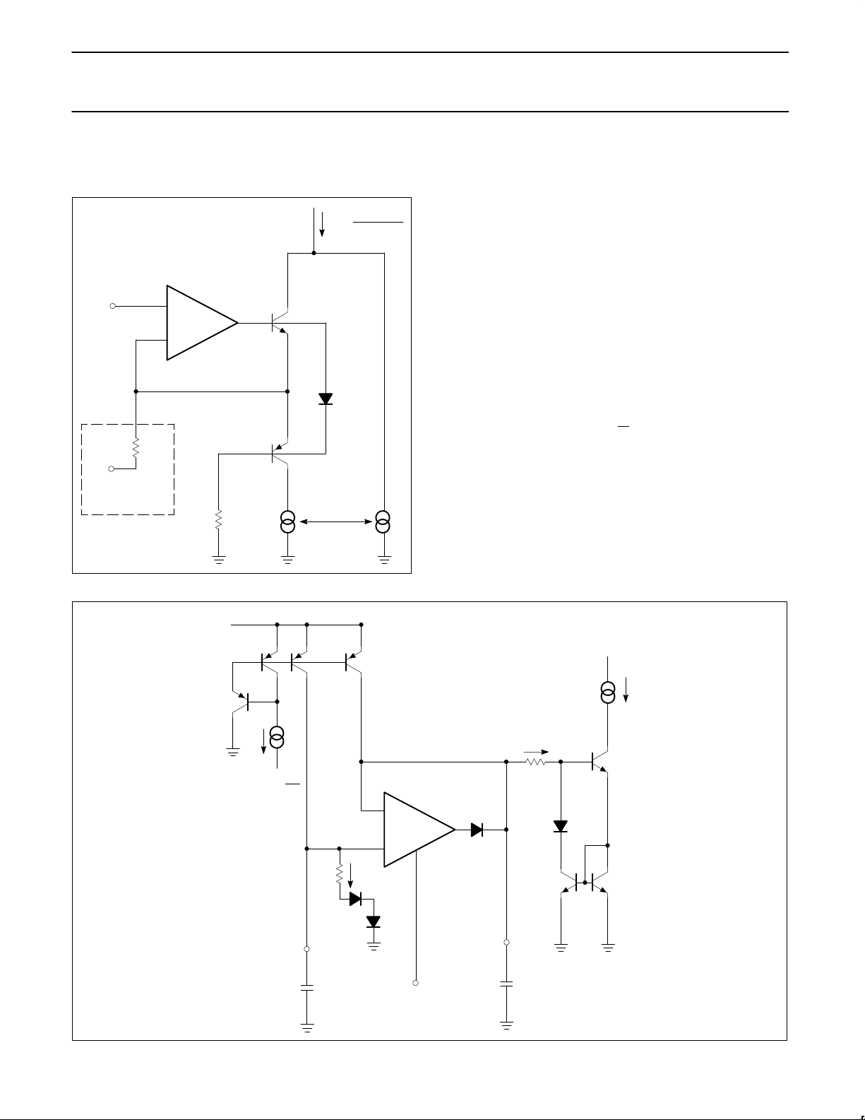
The rectifier is a full-wave design as shown in Figure 5. The input
voltage is converted to current through the input resistor R
turns on either Q
or Q6 depending on the signal polarity. Deadband
5
of the voltage to current converter is reduced by the loop gain of the
gain block A
from input bias current of gain block A
. If AC coupling is used, the rectifier error comes only
2
. The input bias current is
2
typically about 70nA. Frequency response of the gain block A
causes second-order error at high frequency. The collector current
of Q
is mirrored and summed at the collector of Q5 to form the full
6
wave rectified output current I
V
* V
IN
V
R
(AVG)
IN
R
REF
2
2
V+
I
+
R
If V
is AC-coupled, then the equation will be reduced to:
IN
I
+
RAC
. The rectifier transfer function is
R
(4)
and
2
also
2
1987 Oct 7
1
1
I
)
I
G
O
2
2
I
O
Q
Q
4
I
G
3
THD
TRIM
A1
+
V
REF
I
1
140µA
–
Q
1
I
2
2
SR00697
R1
6.8k
Q
280µA
V
IN
Figure 4. Basic Gain Cell Schematic
5
Page 6
Philips Semiconductors Product specification
NE/SA572Programmable analog compandor
The internal bias scheme limits the maximum output current I
to be
R
around 300µA. Within a ±1dB error band the input range of the rectifier
is about 52dB.
VIN* V
REF
R
2
V
V
REF
IN
V+
I
+
R
+
A2
–
R2
Q5
D7
Q6
SR00698
Figure 5. Simplified Rectifier Schematic
Buffer Amplifier
In audio systems, it is desirable to have fast attack time and slow
recovery time for a tone burst input. The fast attack time reduces
transient channel overload but also causes low-frequency ripple
distortion. The low-frequency ripple distortion can be improved with
the slow recovery time. If different attack times are implemented in
corresponding frequency spectrums in a split band audio system,
high quality performance can be achieved. The buffer amplifier is
designed to make this feature available with minimum external
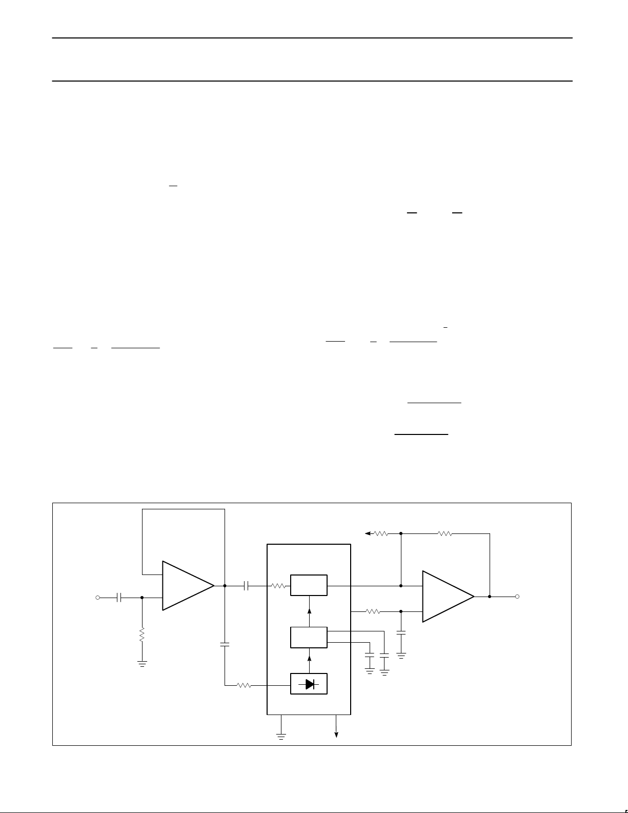
components. Referring to Figure 6, the rectifier output current is
mirrored into the input and output of the unipolar buffer amplifier A
through Q8, Q9 and Q10. Diodes D11 and D12 improve tracking
accuracy and provide common-mode bias for A
positive-going input signal, the buffer amplifier acts like a
voltage-follower . Therefore, the output impedance of A
contribution of capacitor CR to attack time insignificant. Neglecting
diode impedance, the gain Ga(t) for ∆G can be expressed as
follows:
*t
Ga(t) + (Ga
Ga
=Initial Gain
INT
Ga
=Final Gain
FNL
INT
* Ga
FNL
t
e
) Ga
A
τA=RA • CA=10k • CA
FNL
. For a
3
makes the
3
3
Q17
Q8 Q9
V
I
+
R
CA
V+
Q10
I
= 2I
Q
R2
I
R2
IN
R
10k
D11
–
A3
+
I
R1
D12
TRACKING
TRIM
D15
CR
10k
D13
Q14
X2
Q16
X2
Q18
1987 Oct 7
SR00699
Figure 6. Buffer Amplifier Schematic
6
Page 7
Philips Semiconductors Product specification
NE/SA572Programmable analog compandor
where τ
resistor. Diode D
is the attack time constant and RA is a 10k internal
A
opens the feedback loop of A3 for a
15
negative-going signal if the value of capacitor CR is larger than
capacitor CA. The recovery time depends only on CR • R
diode impedance is assumed negligible, the dynamic gain G
. If the
R
(t) for
R
∆G is expressed as follows.
*t
G
(t) + (G
R
GR(t)=(G
* G
RINT
R INT–GR FNL
RFNL
) e +G
t
e
R
R FNL
) G
RFNL
τR=RR • CR=10k • CR
where τR is the recovery time constant and RR is a 10k internal
resistor. The gain control current is mirrored to the gain cell through
Q
. The low level gain errors due to input bias current of A2 and A
14
can be trimmed through the tracking trim pin into A3 with a current
source of ±3µA.
Basic Expandor
Figure 7 shows an application of the circuit as a simple expandor.
The gain expression of the system is given by
R
V
OUT
V
(I
+
IN
=140µA)
1
2
I
Both the resistors R
is a 6.8k internal resistor. The maximum input current into the gain
cell can be as large as 140µA. This corresponds to a voltage level of
140µA • 6.8k=952mV peak. The input peak current into the rectifier
is limited to 300µA by the internal bias system. Note that the value
of R
can be increased to accommodate higher input level. R2 and
1
R
are external resistors. It is easy to adjust the ratio of R3/R2 for
3
desirable system voltage and current levels. A small R
higher gain control current and smaller static and dynamic tracking
error. However, an impedance buffer A
input is voltage drive with large source impedance.
@ V
3
@
1
IN(AVG)
R2@ R
1
and R2 are tied to internal summing nodes. R
1
(5)
results in
2
may be necessary if the
1
The gain cell output current feeds the summing node of the external
OPA A
. R3 and A2 convert the gain cell output current to the output
2
voltage. In high-performance applications, A
has to be low-noise,
2
high-speed and wide band so that the high-performance output of
the gain cell will not be degraded. The non-inverting input of A
2
can
be biased at the low noise internal reference Pin 6 or 10. Resistor
R
is used to bias up the output DC level of A2 for maximum swing.
4
The output DC level of A
+ V
REF
ǒ
1 )
V
ODC
can be tied to a regulated power supply for a dual supply system
V
B
is given by
2
R
3
Ǔ
* V
R
4
R
3
B
(6)
R
4
and be grounded for a single supply system. CA sets the attack time
3
constant and CR sets the recovery time constant. *5COL
Basic Compressor
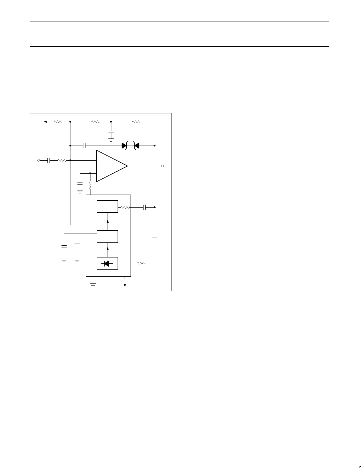
Figure 8 shows the hook-up of the circuit as a compressor. The IC is
put in the feedback loop of the OPA A
is as follows:
V
OUT
V
IN
R
DC1
level of A
1
V
ODC
I
1
+ ǒ
2
, R
, and CDC form a DC feedback for A1. The output DC
DC2
is given by
1
+ V
REF
* V
B
@
ǒ
@
1 )
R
R3@ V
R
DC1
ǒ
@ R
2
IN(AVG)
R
DC1
) R
R
1
) R
R
4
The zener diodes D1 and D2 are used for channel overload
protection.
. The system gain expression
1
1
Ǔ
4
DC2
2
DC2
Ǔ
(7)
(8)
Ǔ
C
V
IN1
IN
2.2µF
1987 Oct 7
R5
100k
R4 R3
+VB
–
A1
+
C
C
IN3
2.2µF
IN2
R2
3.3k
(7,9)
(3,13)
(8)
R1
6.8k
∆
G
BUFFER
(16)
V
REF
(6,10) R6
(4,12)
+V
CC
(5,11)
(2,14)
1k
CA CR
10µF1µF
C1
2.2µF
A2
17.3k
V
OUT
SR00700
Figure 7. Basic Expandor Schematic
7
Page 8
Philips Semiconductors Product specification
NE/SA572Programmable analog compandor
Basic Compandor System
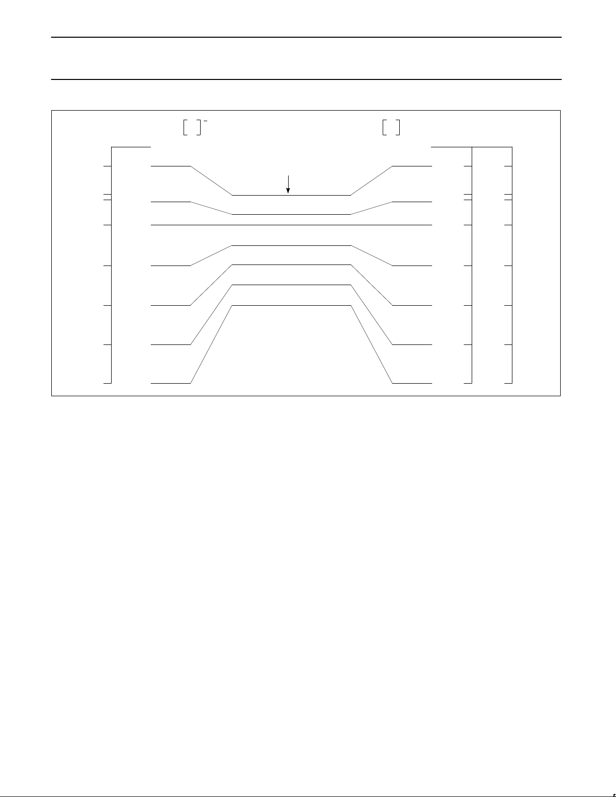
The above basic compressor and expandor can be applied to
systems such as tape/disc noise reduction, digital audio, bucket
brigade delay lines. Additional system design techniques such as
bandlimiting, band splitting, pre-emphasis, de-emphasis and
equalization are easy to incorporate. The IC is a versatile functional
block to achieve a high performance audio system. Figure 9 shows
the system level diagram for reference.
R4 RDC1
9.1k
C2
.1µF
C
IN1
2.2µF
V
IN
R3
17.3k
C1
1k R5
(6,10)
10µF
–
A1
+
V
REF
CDC
RDC2
9.1k
D1
D2
V
OUT
R1
6.8k
(16)
(7,9)
3.3k
R2
(3,13)
CR CA
10µF
(5,11)
(2,14)
(4,12)
1µF
∆
G
BUFFER
(8)
V
CC
Figure 8. Basic Compressor Schematic
C
IN2
2.2µF
C
2.2µF
SR00701
IN3
1987 Oct 7
8
Page 9
Philips Semiconductors Product specification
NE/SA572Programmable analog compandor
V
3.0V
547.6MV
400MV
100MV
10MV
1MV
100µV
10µV
RMS
COMPRESSION
IN
1
2
INPUT TO ∆G
AND RECT
2
EXPANDOR
OUT
REL LEVEL ABS LEVEL
+29.54
+14.77
+12.0
0.0
–20
–40
–60
–80
dB dBM
+11.76
–3.00
–5.78
–17.78
–37.78
–57.78
–77.78
–97.78
SR00702
Figure 9. NE572 System Level
1987 Oct 7
9
Page 10
Philips Semiconductors Product specification
NE/SA572Programmable analog compandor
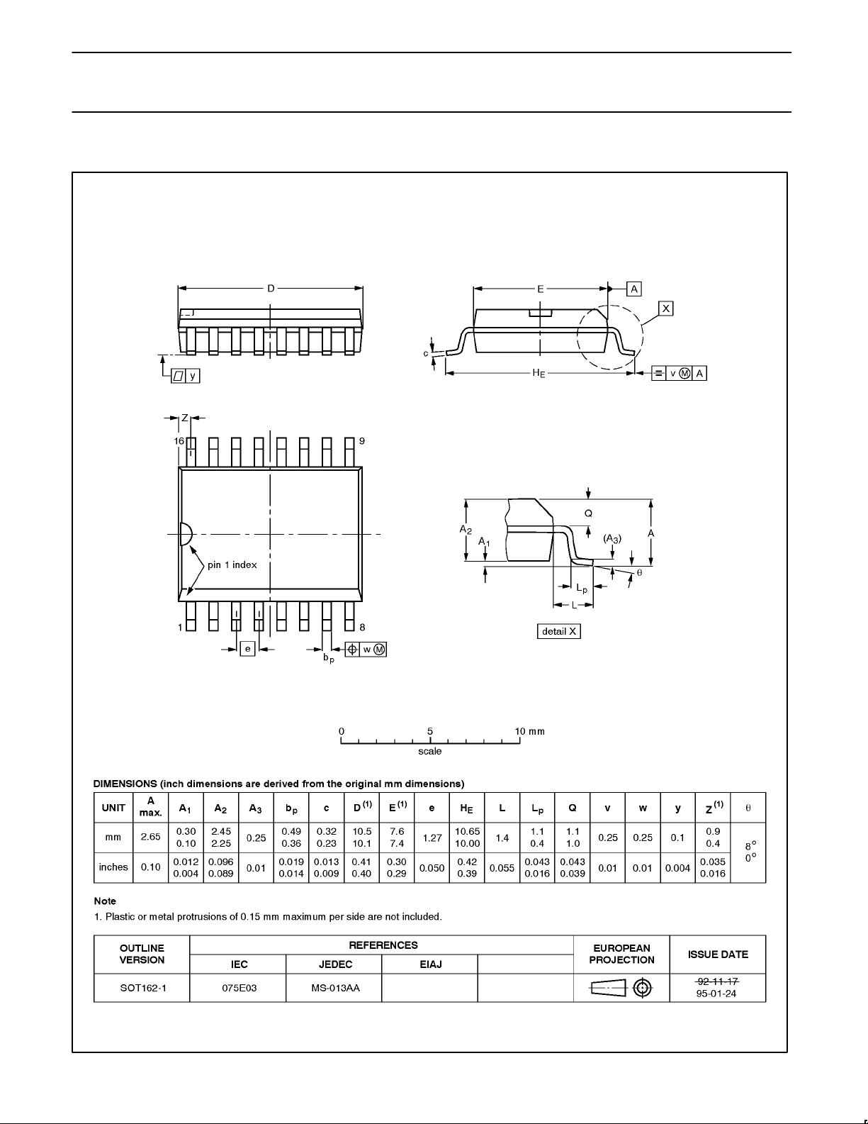
SO16: plastic small outline package; 16 leads; body width 7.5 mm SOT162-1
1987 Oct 7
10
Page 11
Philips Semiconductors Product specification
NE/SA572Programmable analog compandor
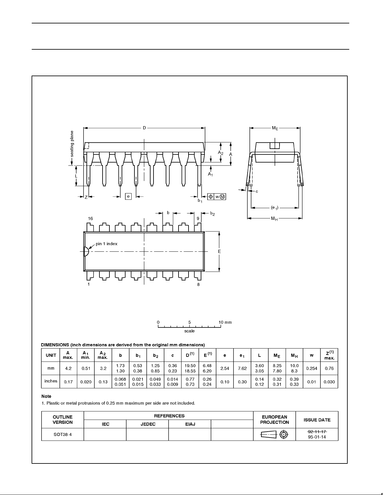
DIP16: plastic dual in-line package; 16 leads (300 mil) SOT38-4
1987 Oct 7
11
Page 12
Philips Semiconductors Product specification
NE/SA572Programmable analog compandor
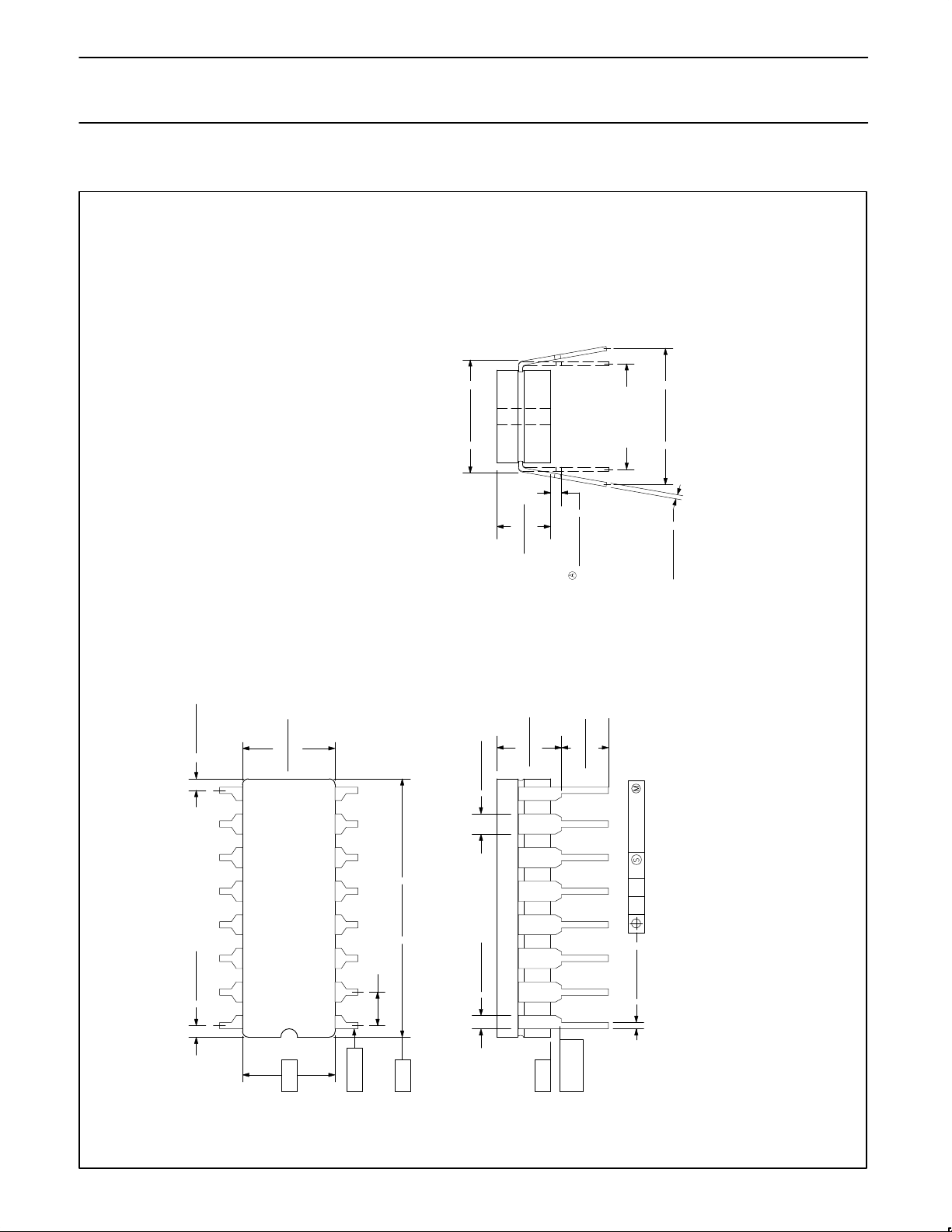
0582B 16-PIN (300 mils wide) CERAMIC DUAL IN-LINE (F) PACKAGE
and include allowance for glass overrun and meniscus
on the seal line, and lid to base mismatch.
constrained to be perpendicular to plane T.
shown in parentheses.
NOTES:
1. Controlling dimension: Inches. Millimeters are
2. Dimension and tolerancing per ANSI Y14. 5M-1982.
3. “T”, “D”, and “E” are reference datums on the body
0.060 (1.52)
0.012 (0.30)
0.306 (7.77)
0.245 (6.22)
counterclockwise to Pin #16 when viewed
from the top.
4. These dimensions measured with the leads
5. Pin numbers start with Pin #1 and continue
(NOTE 4)
0.320 (8.13)
0.290 (7.37)
0.070 (1.78)
0.050 (1.27)
0.175 (4.45)
0.145 (3.68)
0.200 (5.08)
0.165 (4.19)
0.045 (1.143)
0.020 (0.51)
0.165 (4.19)
0.125 (3.18)
BSC
(NOTE 4)
0.300 (7.62)
0.010 (0.254)TED
0.395 (10.03)
0.300 (7.62)
0.015 (0.38)
0.010 (0.25)
0.060 (1.52)
0.012 (0.30)
853-0582B 06688
1987 Oct 7
– E –
0.100 (2.54) BSC
PIN # 1
0.785 (19.94)
0.753 (19.13)
– D –
0.058 (1.47)
0.030 (0.76)
12
0.023 (0.58)
0.015 (0.38)
PLANE
SEATING
– T –
Page 13

Philips Semiconductors Product specification
NE/SA572Programmable analog compandor
DEFINITIONS
Data Sheet Identification Product Status Definition
Objective Specification
Preliminary Specification
Product Specification
Formative or in Design
Preproduction Product
Full Production
This data sheet contains the design target or goal specifications for product development. Specifications
may change in any manner without notice.
This data sheet contains preliminary data, and supplementary data will be published at a later date. Philips
Semiconductors reserves the right to make changes at any time without notice in order to improve design
and supply the best possible product.
This data sheet contains Final Specifications. Philips Semiconductors reserves the right to make changes
at any time without notice, in order to improve design and supply the best possible product.
Philips Semiconductors and Philips Electronics North America Corporation reserve the right to make changes, without notice, in the products,
including circuits, standard cells, and/or software, described or contained herein in order to improve design and/or performance. Philips
Semiconductors assumes no responsibility or liability for the use of any of these products, conveys no license or title under any patent, copyright,
or mask work right to these products, and makes no representations or warranties that these products are free from patent, copyright, or mask
work right infringement, unless otherwise specified. Applications that are described herein for any of these products are for illustrative purposes
only. Philips Semiconductors makes no representation or warranty that such applications will be suitable for the specified use without further testing
or modification.
LIFE SUPPORT APPLICA TIONS
Philips Semiconductors and Philips Electronics North America Corporation Products are not designed for use in life support appliances, devices,
or systems where malfunction of a Philips Semiconductors and Philips Electronics North America Corporation Product can reasonably be expected
to result in a personal injury. Philips Semiconductors and Philips Electronics North America Corporation customers using or selling Philips
Semiconductors and Philips Electronics North America Corporation Products for use in such applications do so at their own risk and agree to fully
indemnify Philips Semiconductors and Philips Electronics North America Corporation for any damages resulting from such improper use or sale.
Philips Semiconductors
811 East Arques Avenue
P.O. Box 3409
Sunnyvale, California 94088–3409
Philips Semiconductors and Philips Electronics North America Corporation
register eligible circuits under the Semiconductor Chip Protection Act.
Copyright Philips Electronics North America Corporation 1996
All rights reserved. Printed in U.S.A.
Telephone 800-234-7381
print code Date of release: 05-96
Document order number:
 Loading...