

Page 1
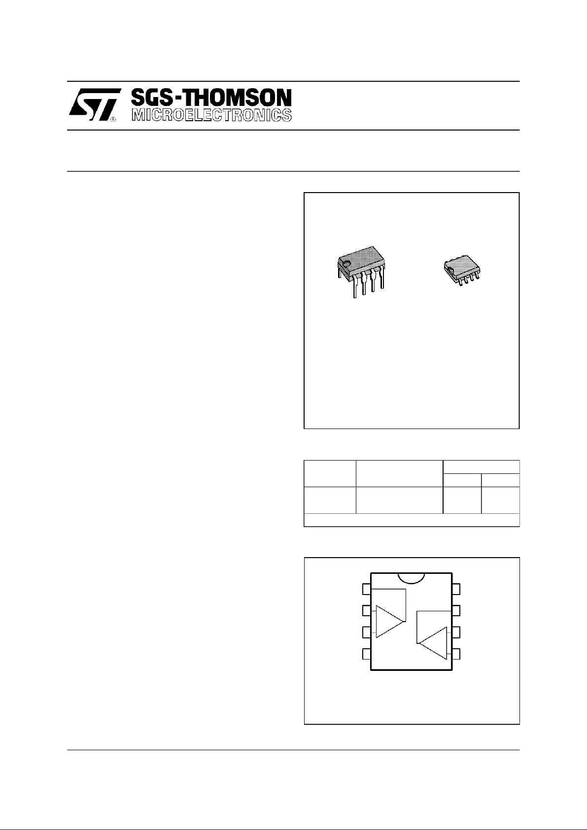
LOW POWER DUAL OPERATIONAL AMPLIFIERS
.INTERNALLYFREQUENCYCOMPENSATED
.LARGEDC VOLTAGE GAIN: 100dB
.WIDEBANDWIDTH (unity gain): 1.1MHz
(temperaturecompensated)
.VERY LOW SUPPLY CURRENT/AMPLI
(500µA) - ESSENTIALLY INDEPENDENT OF
SUPPLYVOLTAGE
.LOWINPUT BIAS CURRENT : 20nA
(temperaturecompensated)
.LOWINPUT OFFSETVOLTAGE: 2mV
.LOWINPUT OFFSETCURRENT: 2nA
.INPUT COMMON-MODE VOLTAGE RANGE
INCLUDESGROUND
.DIFFERENTIAL INPUT VOLTAGE RANGE
EQUALTOTHE POWERSUPPLYVOLTAGE
.LARGE OUTPUT VOLTAGE SWING 0V TO
–1.5V)
(V
CC
NE53 2 - SA53 2
N
DIP8
(Plastic Package)
D
SO8
(PlasticMicropackage)
DESCRIP T ION
Thesecircuitsconsistoftwoindependent,highgain,
internally frequency compensated which were
designedspecificallytooperatefromasinglepower
supplyoverawiderangeofvoltages.Thelowpower
supplydrainis independentofthemagnitudeof the
powersupply voltage.
Applicationareasincludetransduceramplifiers, dc
gainblocksandalltheconventionalop-ampcircuits
whichnowcanbemoreeasilyimplementedinsingle
powersupply systems. For example,thesecircuits
canbedirectlyoperatedoff thestandard+5Vpower
supply voltage which is used in logic systems and
willeasily providetherequiredinterfaceelectronics
withoutrequiringany additionalpowersupply.
In the linearmodetheinput common-modevoltage
range includes ground and the output voltage can
also swing to ground, even though operated from
onlya singlepower supplyvoltage.
The gain-bandwidth product is temperature
compensated.
ORDER CODES
Part
Number
SA532 –40
NE532 0
Example : NE532N
PIN CO NNECT IO NS (top view)
1 - Output 1
2 - Inverting input 1
3 - Non-inverting input 1
-
4-V
CC
Temperature
Range
o
C, +105oC ••
o
C, +70oC ••
1
2
-
+
3
45
-
+
5 - Non-invertinginput 2
6 - Invertinginput 2
7 - Ouput2
8-V
CC
Package
ND
8
7
6
+
September 1995
1/10
Page 2
NE 532 - SA 532
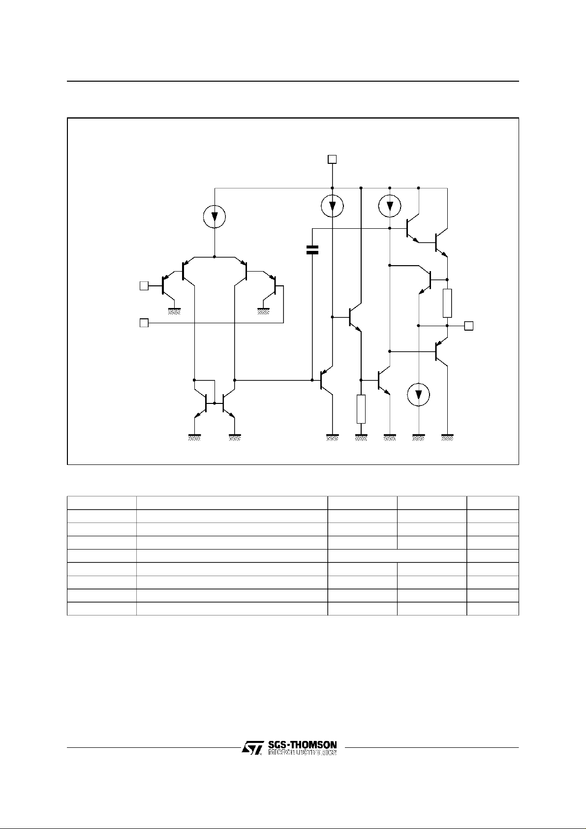
SCHEMATI C DIAGRAM (1/2 NE532-SA532)
V
CC
Inverting
input
Non-inverting
input
Q2
6µA
Q3
Q4Q1
4µA
C
C
100µA
Q5
Q6
Q7
R
SC
Q11
Output
Q13
Q10
Q12
Q8 Q9
50µA
GND
ABSOLUTE MAXIMUM RATINGS
Symbol Parameter SA532 NE532 Unit
V
CC
V
i
V
id
P
tot
I
in
T
oper
T
stg
Notes : 1. This input current only exist when the voltage at any of the input leads is driven negative. It is due to the collec-
2. Short-circuits from the output to V
3. V
4. The direction of the input current is out of the IC. This current is essentially constant, independent of the state of
Supply Voltage +32 +32 V
Input Voltage –0.3 to +32 –0.3 to +32 V
Differential Input Voltage +32 +32 V
Output Short-circuit Duration - (note 2) Infinite
Power Dissipation 500 500 mW
Input Current - (note 1) 50 50 mA
Operating Free-air Temperature Range –40 to +105 0 to +70
Storage Temperature Range –65 to +150 –65 to +150
tor-base junction of the input PNP transistor becoming forward biased and thereby acting as input diode clamps.
In addition to this diode action, there is also NPN parasitic action on the IC chip. This transistor action can cause
the output voltages of the Op-amps to go to the V
duration that an input is driven negative.
This is not destructive and normal output will set up again for input voltage higher than –0.3V.
approximatively 40mA independent of the magnitude of V
short-circuits on all amplifiers.
= 1.4V, RS=0Ω,5V<V
O
the output so no loading change exists on the input lines.
CC
can cause excessive heating if V
CC
+
< 30V, 0 < Vic< V
voltage level (or to ground for a large overdrive) for the time
CC
+
> 15V. The maximum output current is
CC
CC
. Destructive dissipation can result from simultaneous
CC
+
– 1.5V.
o
C
o
C
2/10
Page 3
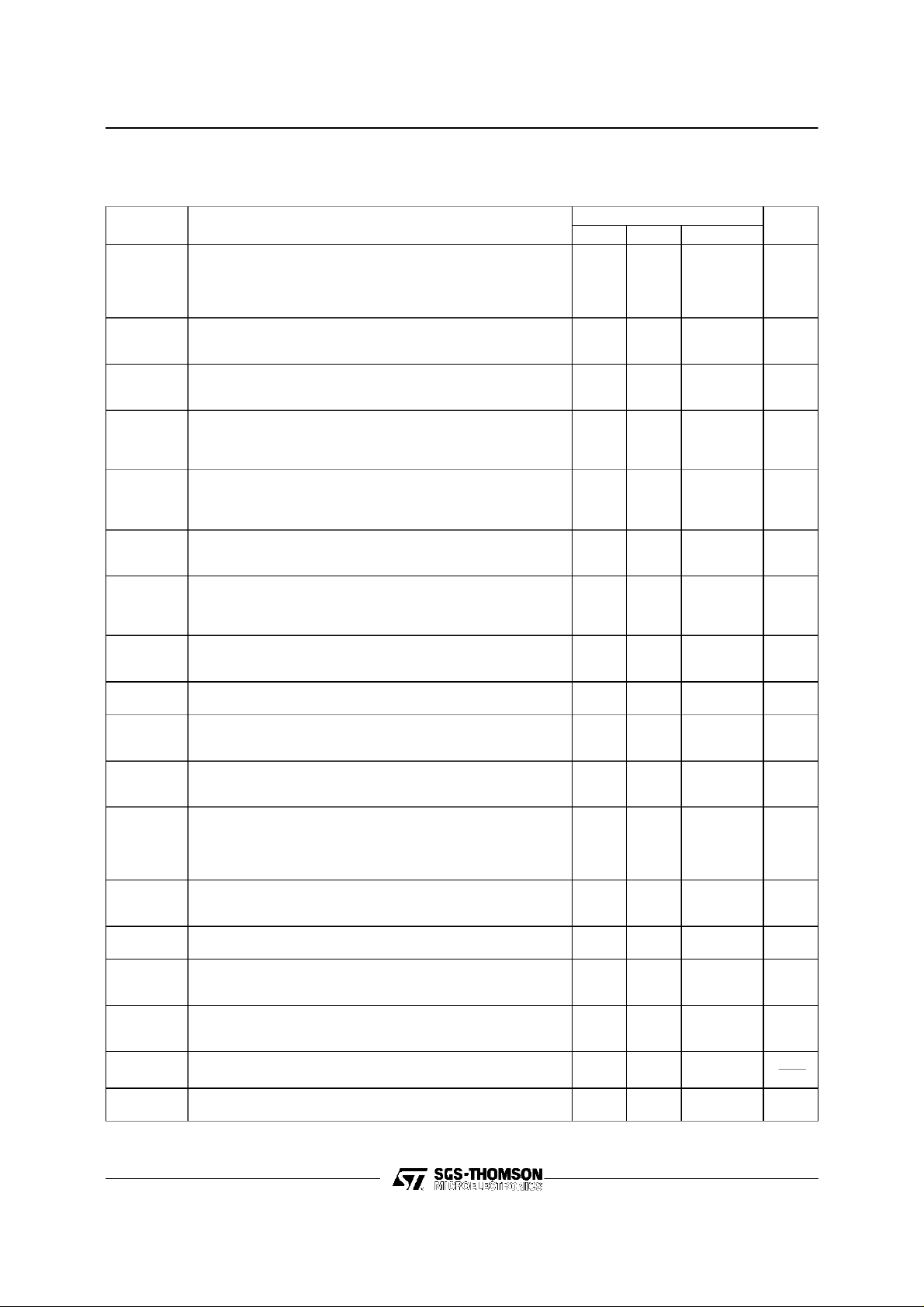
ELECTRICAL CHARACTERISTICS
V
CC
+
= +5V, V
–
= Ground, VO= 1.4V, T
CC
Symbol Parameter
V
io
I
io
I
ib
A
vd
SVR Supply Voltage Rejection Ratio (R
I
CC
V
icm
Input Offset Voltage - (note 3)
=25oC NE532
T
amb
≤ T
≤ T
T
min.
amb
. NE532
max
Input Offset Current
=25oC
T
amb
≤ T
≤ T
T
min.
amb
max
.
Input Bias Current - (note 4)
=25oC
T
amb
≤ T
≤ T
T
min.
amb
max
.
Large Signal Voltage Gain
= +15V, RL=2kΩ,VO= 1.4V to 11.4V)
(V
CC
=25oC
T
amb
≤ T
≤ T
≤ T
max
max
.
.
(V
CC
T
min.
+
= 5 to 30V)
=25oC
T
amb
≤ T
T
min.
amb
amb
Supply Current, all Amp, no Load
V
CC
V
CC
= +5V, T
= +30V, T
min.
min.
≤ T
≤ T
amb
amb
≤ T
Input Common Mode Voltage Range
= +30V) - (note 6)
(V
CC
=25oC
T
amb
T
min
. ≤ T
amb
≤ T
max
.
CMR Common-mode Rejection Ratio (R
=25oC
T
amb
≤ T
≤ T
T
min.
I
O
I
sink
V
OPP
V
OH
V
OL
Output Short Circuit Current
= +15V, Vo= 2V, Vid= +1V) 20 40 60
(V
CC
Output Current Sink (Vid= -1V)
= +15V, VO=2V
V
CC
= +15V, VO= +0.2V
V
CC
Output Voltage Swing (RL=2kΩ)
=25oC
T
amb
≤ T
T
min.
High Level Output Voltage (V
=25oCR
T
amb
. ≤ T
T
min
=25oCR
T
amb
≤ T
T
min.
Low Level Output Voltage (RL= 10kΩ)
=25oC
T
amb
. ≤ T
T
min
SR Slew Rate (V
100pF, T
amb
amb
amb
amb
amb
amb
CC
=25oC, unity gain) 0.3 0.6
.
max
≤ T
.
max
≤ T
.
max
≤ T
.
max
≤ T
max.
= 15V, VI= 0.5 to 3V, RL=2kΩ,CL=
GBP Gain Bandwidth Product
= 30V, f = 100kHz, T
(V
CC
= 10mV, RL=2kΩ,CL= 100pF) 0.7 1.1
V
in
amb
THD Total Harmonic Distortion
= 20dB, RL=2kΩ,VCC= 30V,
v
=25oC, VO=2PP)
amb
= 100Ω,VCC= 30V) 45
s
= 100 120
V
O1/VO2
(f = 1kHz, A
= 100pF, T
C
L
e
n
Equivalent Input Noise voltage
(f = 1kHz, R
Channel Separation
A
V
max
≤ T
max
+
= 30V)
CC
=25oC,
=25oC (unless otherwise specified)
amb
Min. Typ. Max.
SA532
SA532
50
25
= 10kΩ)
S
65
65
.
.
0
0
= 10kΩ)
S
70
60
10
12
0
0
=2kΩ
L
= 10kΩ
L
26
26
27
27
NE532 - SA532
NE532 - SA532
27
230
20 150
100
100
0.7 1.2
85
20
50
27
28
520
0.02
200
V
CC
V
CC
V
CC
V
CC
5
9
7
40
2
+
–1.5
+
–2
+
–1.5
+
–2
20
Unit
mV
nA
nA
V/mV
dB
mA
V
dB
mA
mA
µA
V
V
mV
V/µs
MHz
%
nV
√Hz
dB
3/10
Page 4
NE532 - SA532
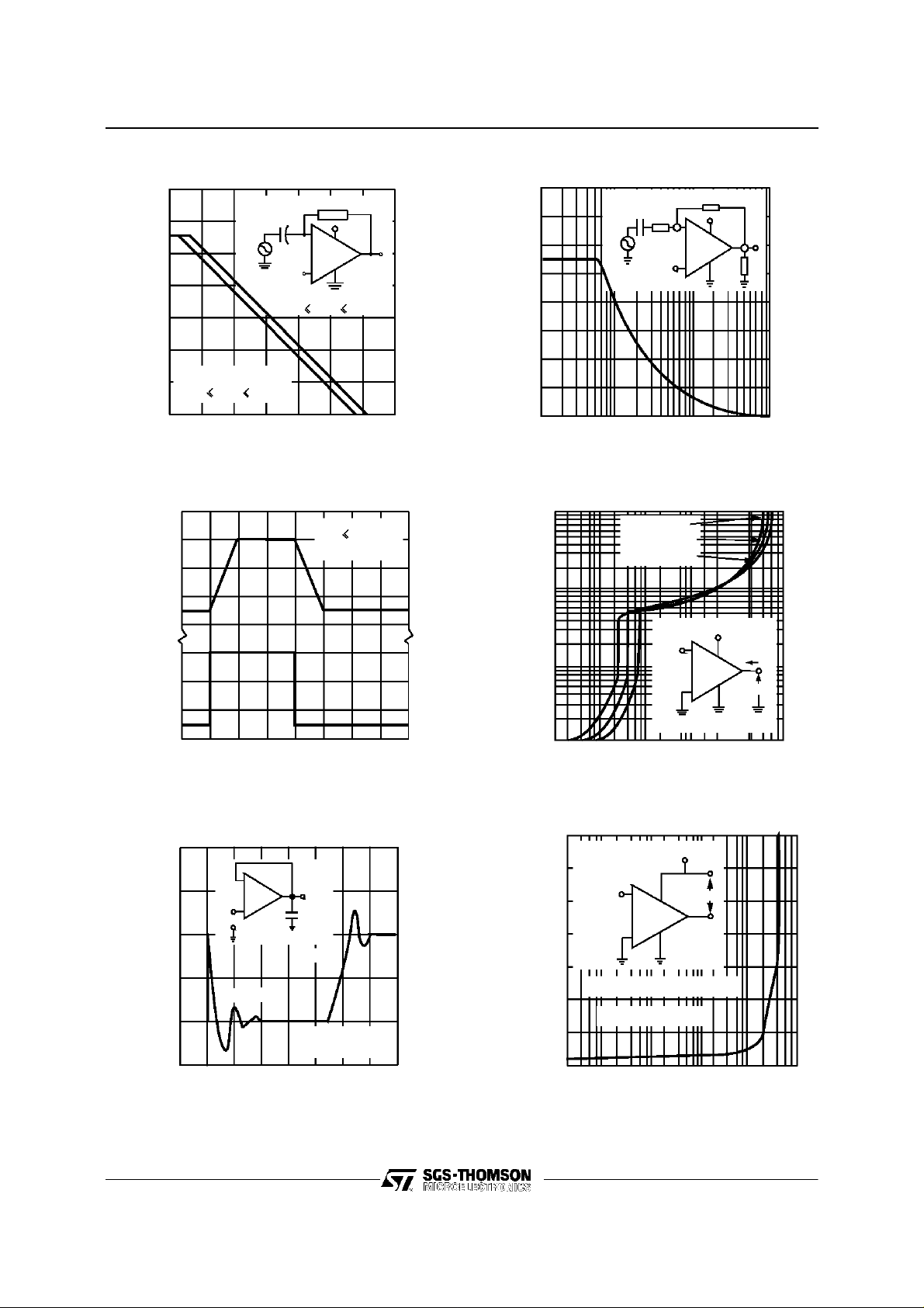
OPEN LOOP FREQUENCY RESPONSE (NOTE 3)
140
120
100
80
60
40
0.1µF
V
I
10M
-
VCC/2
+
VCC= 30V&
T
-55 C
amb
Ω
V
CC
+125 C
V
O
VOLTAGE GAIN (dB)
20
VCC= +10 to + 15V &
T
amb
+125 C
-55 C
0
1.0 10 100 1k 10k 100k 1M 10M
FREQUENCY (Hz)
VOLTAGE FO LLOWER PU LSE R E S P O NS E
4
RL 2 k
3
Ω
VCC = + 15 V
2
OUTPUT
1
VOLTAGE (V)
0
3
2
1
INPUT
010203040
VOLTAGE (V)
(
TIME
s)
µ
LARGE SIGNAL F RE Q UE NC YR E S P O NS E
20
1k
15
V
I
+7V
10
5
OUTPUT SWING (Vpp)
0
1k 10k 100k 1 M
100k
Ω
Ω
+15 V
-
+
VO
2k
Ω
FR EQ UE NC Y (Hz)
OUTPUT C HARACTE RIS TICS
10
VC C = +5 V
VCC = + 15V
VCC = + 30V
1
v
T
-
+
amb
cc
=+25 C
I
O
V
O
vcc/2
0.1
OUTPUT VOLTAGE (V)
0.01
0,001 0,01 0,1 1 10 100
OUTPUT S INK C UR RE NT (m A)
VOLTAGE FOLLOWER PULSE RESPONSE
(SMAL LSIGNAL)
500
e
l
Output
+
e
-
O
50pF
Input
T
amb
VCC=30V
450
400
350
OUTPUT VOLTAGE (mV)
300
250
012345678
TIME (µs)
4/10
=+25 C
OUTPUT CHARACTERISTICS
8
7
VCC/2
6
(V)
5
+
CC
4
TO V
Independent ofV
3
2
OUTPUT VOLTAGE REFERENCED
1
0,001
OUTPUTSOURCE CU RRENT (mA)
V
CC
+
-
V
O
I
O
CC
T
=+25 C
amb
0,01 0,1 1 10 100
Page 5
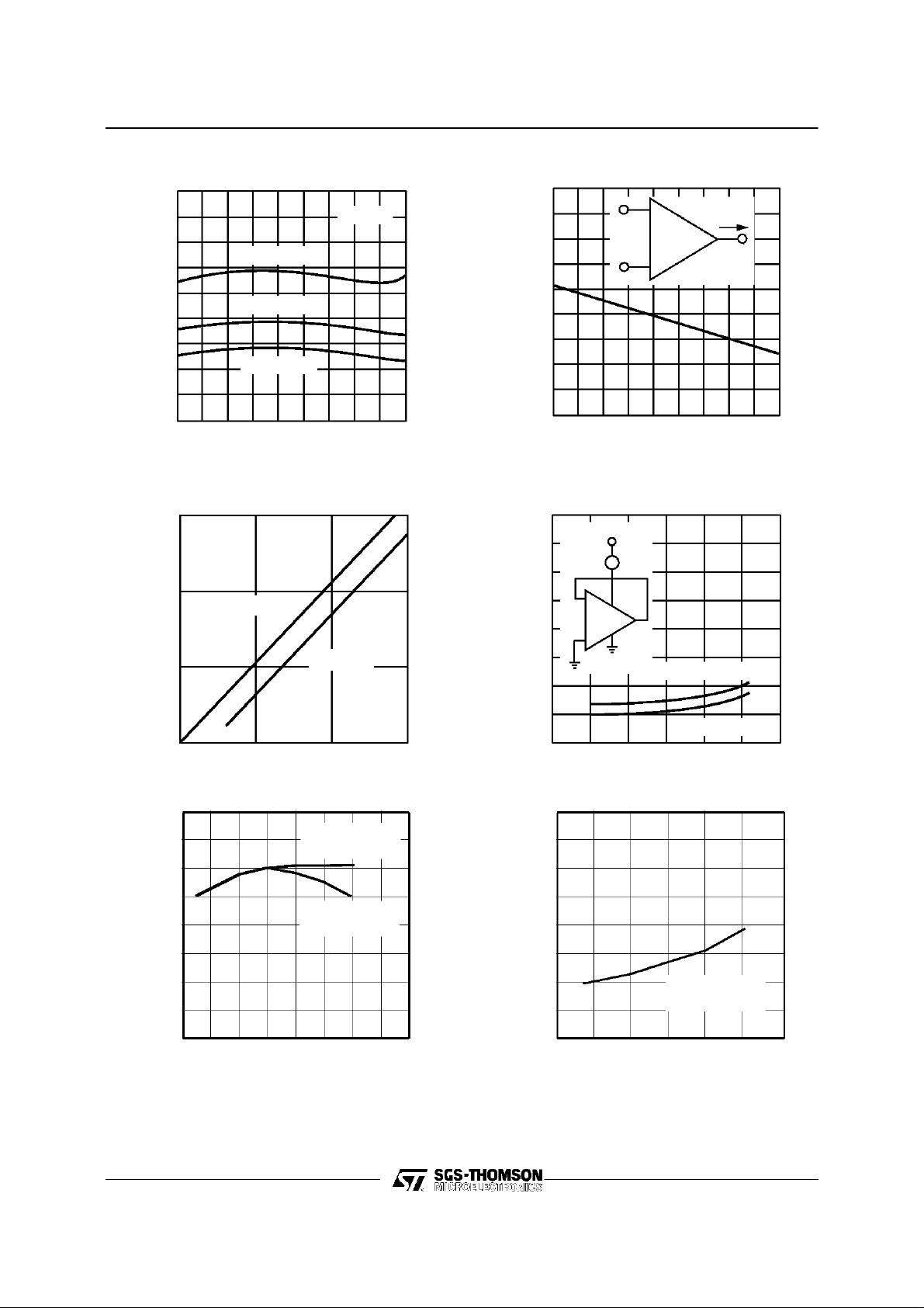
NE532 - SA532
INPUT CURRENT (Note 1)
90
80
70
60
50
40
30
20
INPUT CURRENT (mA)
10
0
-55 -35 -15 5 25 45 65 85 105 125
VCC=+30V
VCC=+15V
VCC=+5V
VI=0V
TEMP ER ATURE ( C )
INPUT VOLTAGE R ANGE
15
10
NØga tive
5
P os itive
INPUT VOLTAGE (V)
0 5 10 15
P OWER S UPPLY VOLTAGE (– V)
CURR E NT LIMITING (No te 1)
90
80
70
60
50
40
30
20
OUTPUT CURRENT (mA)
10
0
-55 -35 -15 5 25 45 65 85 105 125
-
+
I
O
TEMPE RATURE ( C)
SUPPLY CURRENT
4
V
CC
I
3
2
1
mA
D
-
+
T
= 0 C to +125 C
amb
SUPPLY CURRENT (mA)
T
=-55 C
amb
0102030
P OSITIVE S UP PLY VOLTAGE (V)
160
R=20k
L
Ω
120
80
R=2k
L
Ω
40
VOLTAGE GAIN (dB)
010203040
P OSITIVE S UPP LY VOLTAGE (V)
100
75
50
25
INPUT CURRENT (nA)
T = +2 5 C
amb
0102030
POSITIVE SUPPLYVOLTAGE (V)
5/10
Page 6
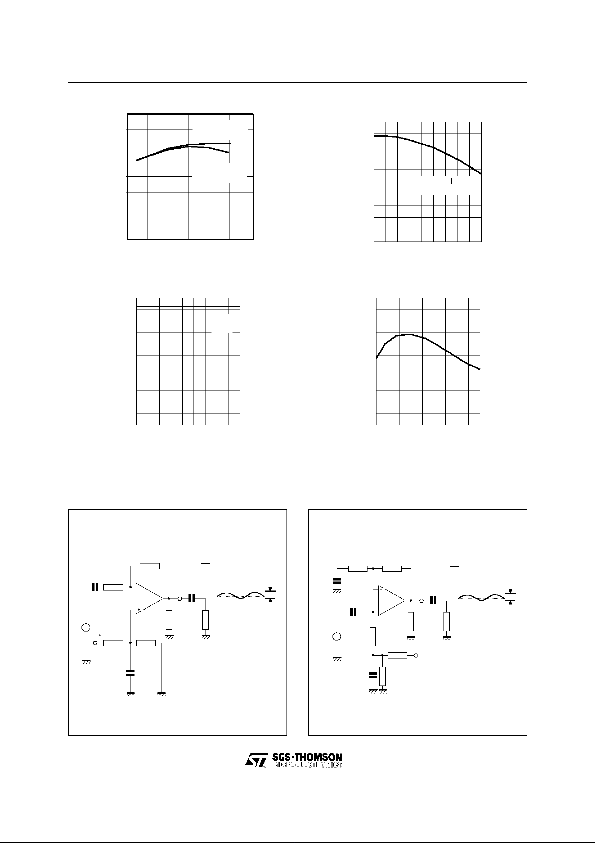
NE532 - SA532
160
R=20k
Ω
L
120
VOLTAGE GAIN (dB)
80
40
R=2k
L
Ω
0102030
P OS ITIVE S UPP LYVOLTAGE (V)
115
110
105
SVR
100
95
90
85
80
75
70
65
-55-35-15 5 25 45 65 85 105 125
60
POWER SUPPLY REJECTION RATIO (dB)
TEMP ER ATURE ( C )
1.5
1.35
1.2
1.05
0.9
0.75
V = 15V
CC
0.6
0.45
0.3
0.15
0
GAIN BANDWIDTH PRODUCT (MHz)
-55-35-15 5 25 45 65 85 105 125
TEMP ER ATURE ( C )
115
110
105
100
95
90
85
80
75
70
65
-55-35-15 5 25 45 65 85 105 125
60
COMMON MODE REJECTION RATIO (dB)
TEMP ER ATURE ( C )
TYPICAL APPLICATIONS (single supply voltage) VCC=+5V
AC COUPLED INVERTING AMPLIFIER
R
f
e
6/10
100k
Ω
R1
C
10k
I
Ω
1/2
NE532
R
B
6.2 k
I
~
R2
100 k
Ω
V
CC
C1
F
10
µ
R3
100k
Ω
Ω
R
f
A=-
V
R1
(as shown A = -10)
V
C
o
0
e
o
R
L
10k
Ω
2V
PP
AC COUP LE D NO N-INV ERTING AM PLIFIE R
R1
100k
C1
0.1µF
C
I
e
R3
I
1M
~
C2
10
DC
R2
1M
Ω
µ
Ω
1/2
NE532
R
B
6.2k
Ω
Ω
R4
100k
Ω
V
CC
R5
100k
F
Ω
R2
A=1+
V
R1
(as s hown A = 11)
V
C
o
0
e
o
R
L
10k
Ω
2V
PP
Page 7
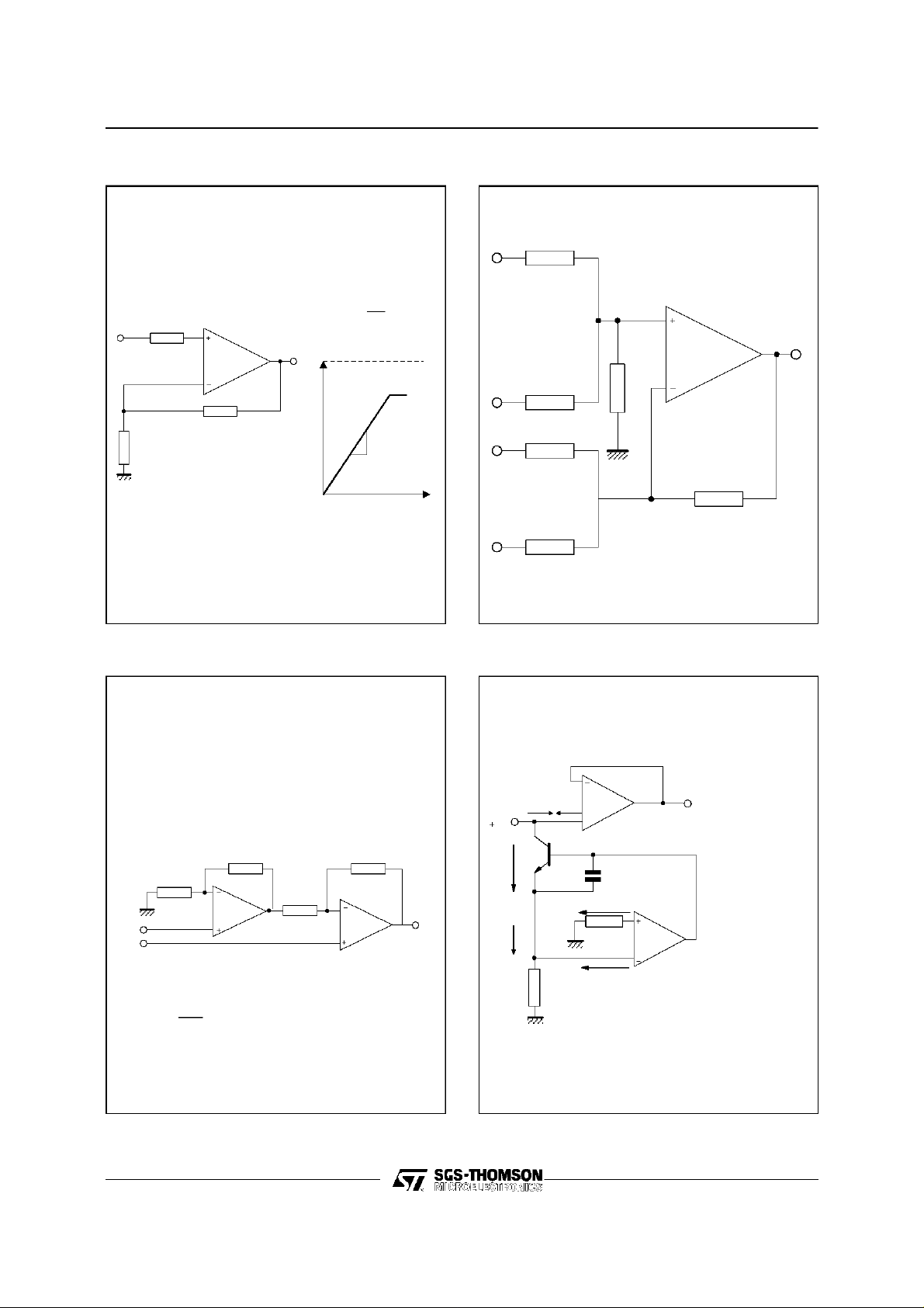
NE532 - SA532
NON-IN VE RTI NG DC A MP L IFIER
=1+
A
V
(As shown = 101)A
e
O
+5V
(V)
O
e
0
10k
R1
10k
Ω
1/2
NE532
R2
1M
Ω
Ω
DC SUMMI NG A MPL I FIER
e
100k
1
R2
R1
V
e
2
e
3
e
(mV)
I
e
4
100k
100k
100k
Ω
100k
Ω
Ω
Ω
Ω
eo=e1+e2-e3-e
where(e1+e2)≥(e3+e4)
to keep e
≥ 0V
o
1/2
NE532
100k
e
O
Ω
4
HIGH INPUT Z, DC DIFFERENTIAL
AMPLIFIER
R2
100k
1/2
NE532
Ω
R1
100k
Ω
+V1
+V2
if R1=R5andR3=R4=R6=R
2R
eo=[1+
As shown e
1
] (e2± e1)
R
2
= 101 (e2-e1).
o
R3
100k
Ω
7
R4
100k
1/2
NE532
USING SYMMETRICAL AMPLIFIERS TO
REDUCE I NPU T CURRENT
I
e
I
I
B
Ω
I
2N 929
NE532
B
1/2
I
0.001µF
I
3M
B
1/2
Ω
NE532
I
B
I
1.5M
B
Ω
V
o
e
o
Input current compensation
7/10
Page 8
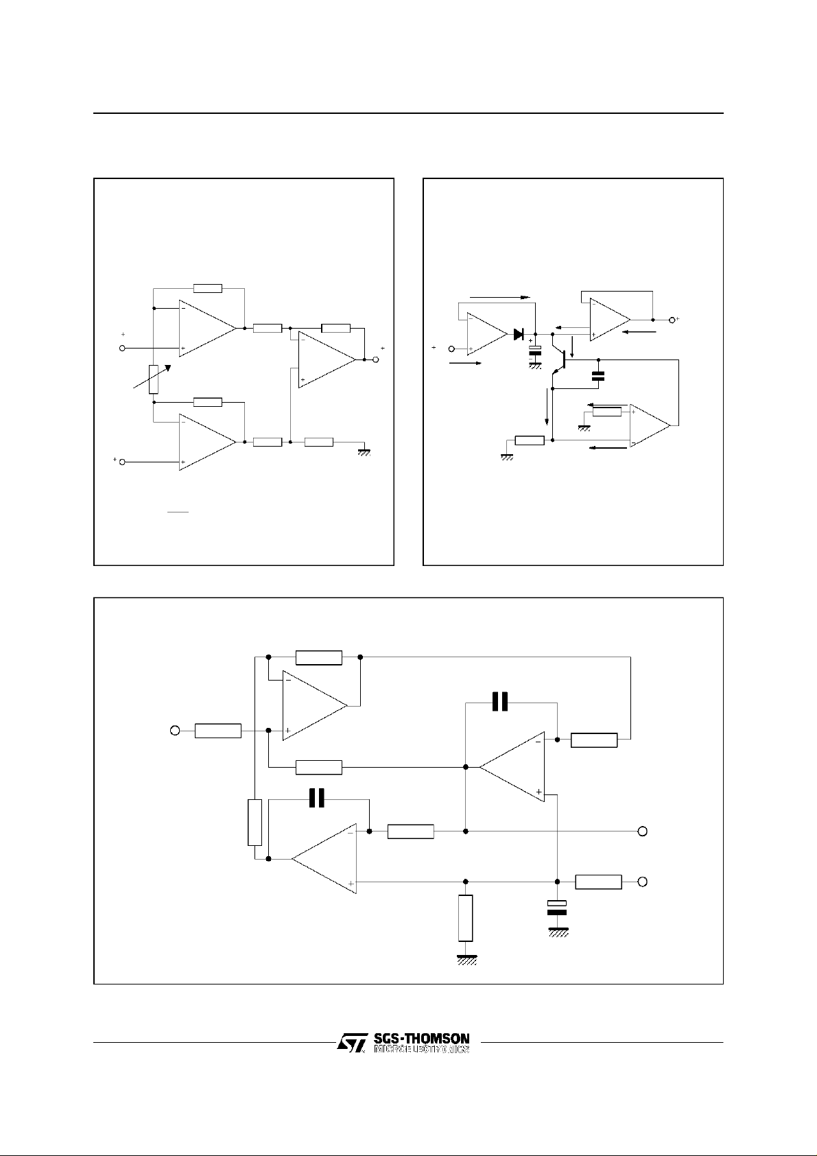
NE 532 - SA 532
HIGH INPUT Z ADJUSTABLE GAIN DC
INSTRUMENTATION AMPLIFIER
R1
100k
Ω
1/2
NE532
R7
100k
R4
100k
Ω
Ω
1/2
e
1
R2
2k
Ω
e
2
NE532
Ga in adjust
100k
1/2
NE532
R5
Ω
if R1=R5and R3=R4=R6=R
2R
eo=[1+
As showne
1
] (e2± e1)
R
2
=101 (e2-e1)
o
R3
100k
R6
100k
Ω
Ω
7
LOW DRIFT PEAK DETECTOR
I
B
1/2
I
B
2I
2N 929
B
NE532
0.001µF
I
B
3R
3M
Ω
I
B
Z
NE532
1/2
NE532
e
e
O
I
Z
I
1µF
1M
C
2I
B
R
Ω
o
1/2
Input current
compensation
e
o
ACTIVE BAND-PASS FILTER
R2
100k
Ω
NE532
+V1
R3
100k
Ω
Fo= 1kHz
Q=50
=100 (40dB)
A
V
R1
100k
1/2
R4
10M
1/2
NE532
Ω
Ω
C2
330pF
R6
470k
Ω
R8
100k
Ω
C1
330pF
1/2
NE532
10µF
C3
R5
470k
R7
100k
Ω
Ω
V
V
o
CC
8/10
Page 9
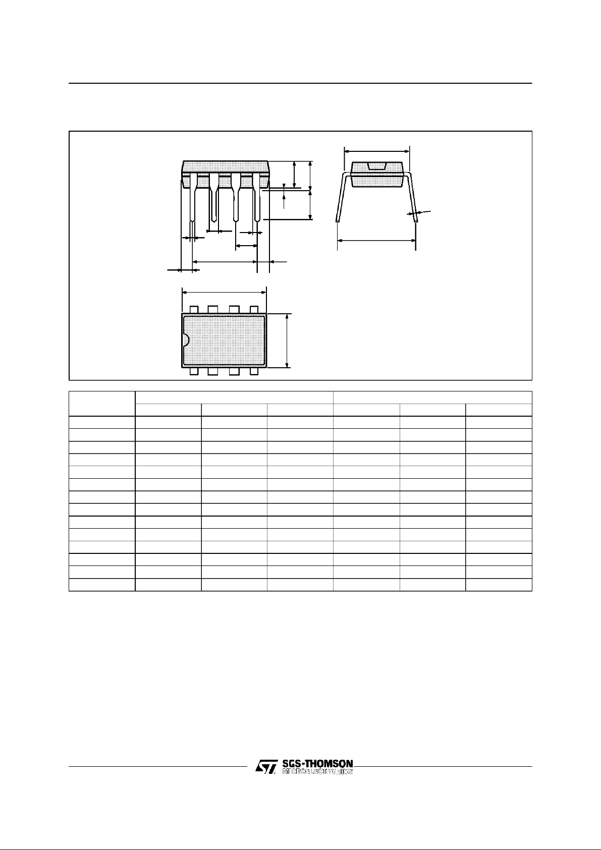
PACKAGE MECHANICAL DATA
8 PINS - PLASTIC DIP OR CERDIP
B
b
Z
e3
D
B1
NE532 - SA532
e4
I
A
L
a1
e
Z
E
b1
Dimensions
8
14
Millimeters Inches
Min. Typ. Max. Min. Typ. Max.
5
F
A 3.32 0.131
a1 0.51 0.020
B 1.15 1.65 0.045 0.065
b 0.356 0.55 0.014 0.022
b1 0.204 0.304 0.008 0.012
D 10.92 0.430
E 7.95 9.75 0.313 0.384
e 2.54 0.100
e3 7.62 0.300
e4 7.62 0.300
F 6.6 0260
i 5.08 0.200
L 3.18 3.81 0.125 0.150
Z 1.52 0.060
PM-DIP8.EPS
DIP8.TBL
9/10
Page 10
NE 532 - SA 532
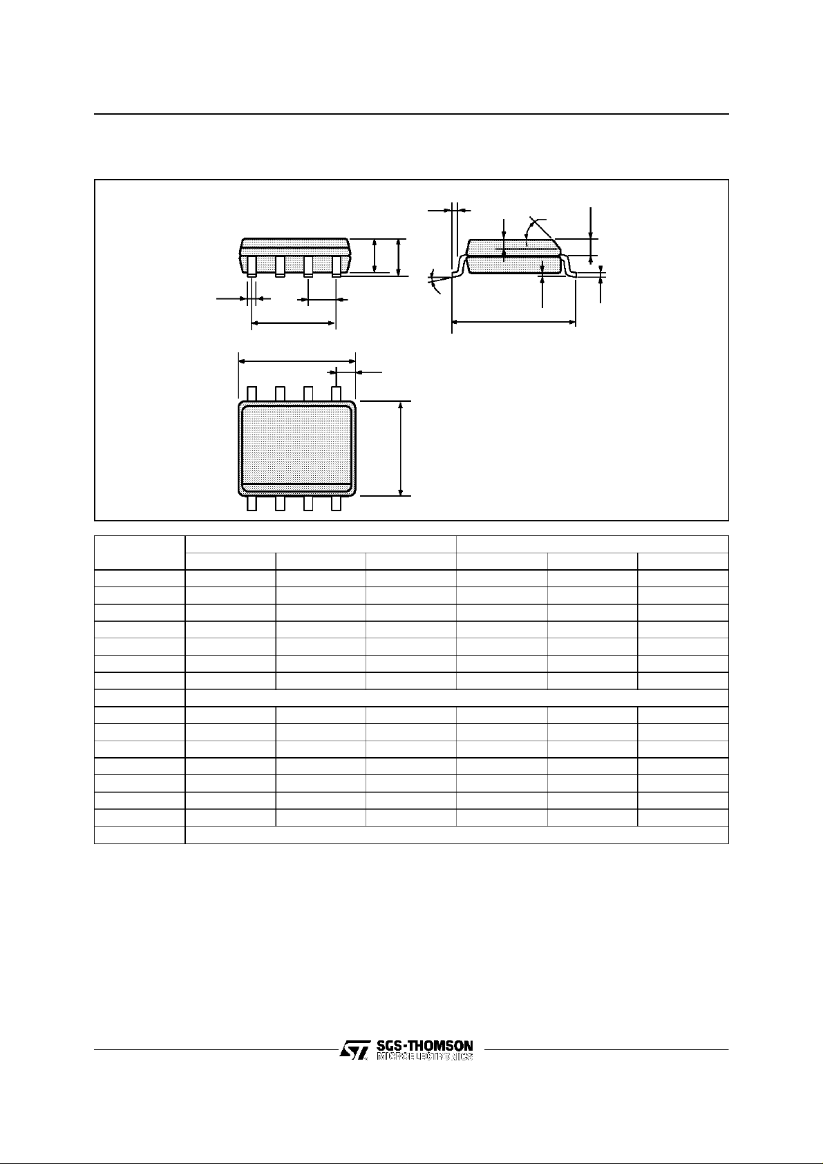
PACKAGE MECHANICAL DATA
8 PINS - PLASTIC MICROPACKAGE (SO)
a2
L
c1
C
A
a3
e
e3
D
M
5
s
F
a1
E
b1
Millimeters Inches
Dimensions
b
8
14
Min. Typ. Max. Min. Typ. Max.
A 1.75 0.069
a1 0.1 0.25 0.004 0.010
a2 1.65 0.065
a3 0.65 0.85 0.026 0.033
b 0.35 0.48 0.014 0.019
b1 0.19 0.25 0.007 0.010
C 0.25 0.5 0.010 0.020
c1 45
o
(typ.)
D 4.8 5.0 0.189 0.197
E 5.8 6.2 0.228 0.244
e 1.27 0.050
e3 3.81 0.150
F 3.8 4.0 0.150 0.157
L 0.4 1.27 0.016 0.050
M 0.6 0.024
S8
o
(max.)
PM-SO8.EPS
SO8.TBL
Information furnished is believed to be accurate and reliable. However, SGS-THOMSON Microelectronics assumes no responsibility for the consequences of use of such information nor for any infringement of patents or other rights of third parties which
may result from its use. No licence is granted by implication or otherwise under any patent or patent rights of SGS-THOMSON
Microelectronics. Specifications mentioned in this publication are subject to change without notice. This publication supersedes
and replaces all information previously supplied. SGS-THOMSON Microelectronics products are not authorized for use as critical
components in life support devices or systems without express written approval of SGS-THOMSON Microelectronics.
1995SGS-THOMSON Microelectronics - All Rights Reserved
SGS-THOMSON Microelectronics GROUP OF COMPANIES
Australia - Brazil - France - Germany - Hong Kong - Italy - Japan - Korea - Malaysia - Malta - Morocco - The Netherlands
Singapore - Spain - Sweden - Switzerland - Taiwan - Thailand - United Kingdom - U.S.A.
10/10
ORDERCODE :
 Loading...