

Page 1

NE1617
Temperature monitor for
microprocessor systems
Product specification 1999 Mar 19
INTEGRATED CIRCUITS
Page 2
Philips Semiconductors Product specification
NE1617Temperature monitor for microprocessor systems
2
1999 Mar 19 853–2144 21065
FEA TURES
•Replacement for Maxim MAX1617 and Analog Devices ADM1021
•Monitors local and remote temperature
•Accuracy
– ± 2°C local (on-chip) sensor
– ± 3°C remote sensor
•No calibration required
•Programmable over/under temperature alarm
•SMBus 2-wire serial interface
•3V to 5.5V supply range
•70µa supply current in operating mode
•3µa (typical) supply current in standby mode
•Small 16–lead QSOP package
APPLICATIONS
•Desktop computers
•Notebook computers
•Smart battery packs
•Industrial controllers
•T elecom equipment
DESCRIPTION
The NE1617 is an accurate two-channel temperature monitor. It
measures the temperature of itself and the temperature of a remote
sensor. The remote sensor is a diode connected transistor. This can
be in the form of either a discrete NPN/PNP, such as the
2N3904/2N3906, or a diode connected PNP built into another die,
such as is done on some INTEL microprocessors.
The temperature of both the remote and local sensors is stored in a
register that can be read via a 2-wire SMBus. The temperatures are
updated at a rate that is programmable via the SMBus (the average
supply current is dependent upon the update rate—the faster the
rate, the higher the current).
In addition to the normal operation, which is to update the
temperature at the programmed rate, there is a one shot mode that
will force a temperature update.
There is also an alarm that senses either an over or under
temperature condition. The trip points for this alarm are also
programmable.
The device can have 1 of 9 addresses (determined by 2 address
pins), so there can be up to 9 of the NE1617 on the SMBus.
It can also be put in a standby mode (in order to save power). This
can be done either with software (over the SMBus) or with hardware
(using the STANDBY pin).
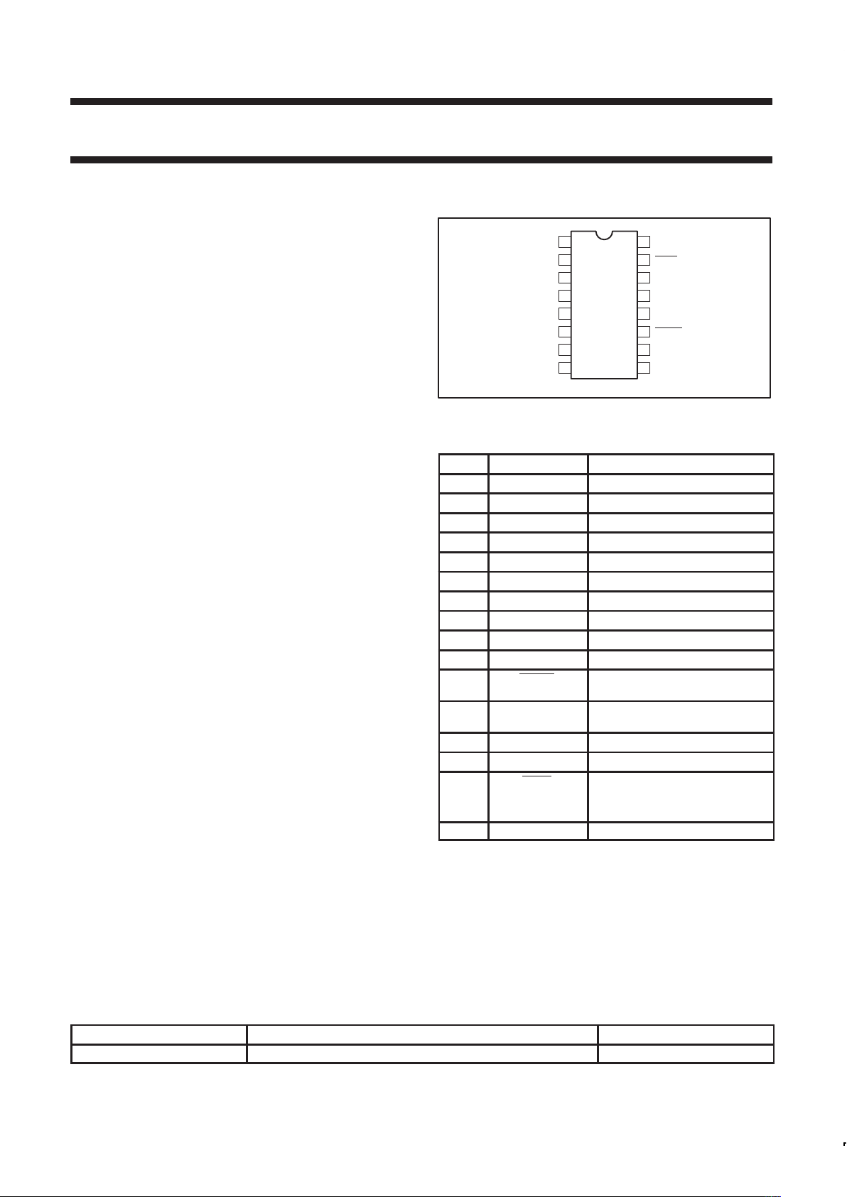
PIN CONFIGURATION
9
10
11
12
13
14
15
161
2
3
4
5
6
7
8
TEST
V
DD
D+
D–
TEST
ADD1
GND
GND
TEST
STBY
SCLK
TEST
SDATA
ALERT
ADD0
TEST
SL01202
Figure 1. Pin configuration
PIN FUNCTION DESCRIPTION
PIN # FUNCTION DESCRIPTION/COMMENTS
1 TEST Factory use only
1
2 V
DD
Positive supply
2
3 D+ Positive side of remote sensor
4 D– Negative side of remote sensor
5 TEST Factory use only
1
6 ADD1 Device address pin (3-State)
7 GND Ground
8 GND Ground
9 TEST Factory use only
1
10 ADD0 Device address pin (3-State)
11 ALERT Open drain output used as
interrupt or SMBus alert
12 SDATA SMBus serial data input/output
open drain
13 TEST Factory use only
1
14 SCLK SMBus clock input
15 STBY Hardware standby input pin
HIGH = normal operating mode
LOW = standby mode
16 TEST Factory use only
1
NOTES:
1. These pins should either float or be tied to ground.
2. VDD pin should be decoupled by a 0.1µF capacitor.
ORDERING INFORMATION
PART NUMBER PACKAGE DRAWING NUMBER
NE1617DS 16-lead QSOP package SOT519–1
Page 3
Philips Semiconductors Product specification
NE1617Temperature monitor for microprocessor systems
1999 Mar 19
3
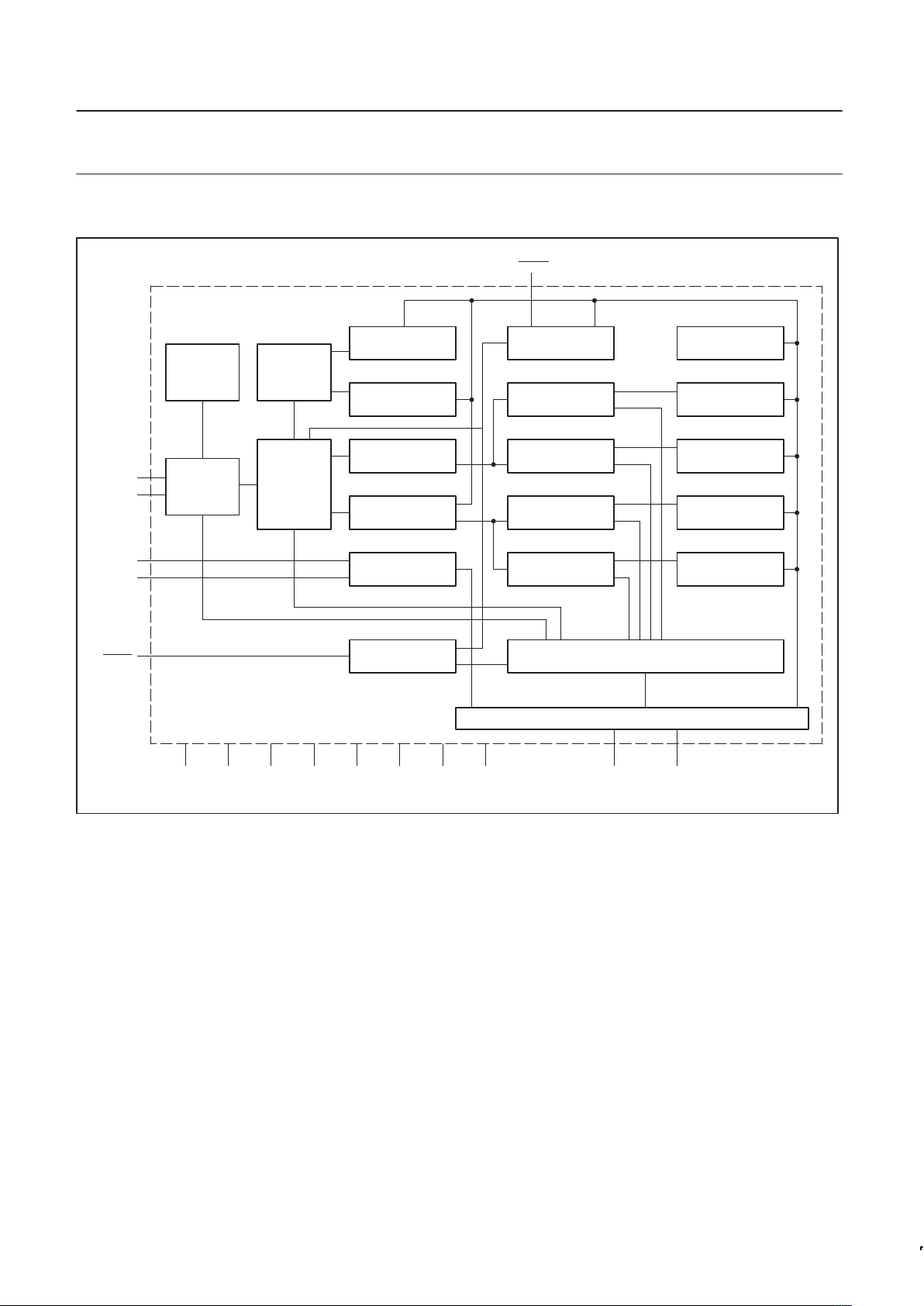
FUNCTIONAL BLOCK DIAGRAM
COMMAND POINTER
REGISTER
LOCAL TEMP HIGH
LIMIT REGISTER
LOCAL TEMP LOW
LIMIT REGISTER
REMOTE TEMP HIGH
LIMIT REGISTER
REMOTE TEMP LOW
LIMIT REGISTER
CONFIGURATION
REGISTER
LOCAL TEMP HIGH
THRESHOLD
LOCAL LOW TEMP
THRESHOLD
REMOTE HIGH TEMP
THRESHOLD
REMOTE LOW TEMP
THRESHOLD
STATUS REGISTER
SMBUS INTERFACE
ONE-SHOT
REGISTER
CONVERSION RATE
REGISTER
LOCAL TEMP
DATA REGISTER
REMOTE TEMP
DATA REGISTER
ADDRESS
DECODER
INTERRUPT
MASKING
A-TO-D
CONVERTER
CONTROL
LOGIC
LOCAL TEMP
SENSOR
ANALOG
MUX
ALERT
ADD0
ADD1
D–
D+
STDBY
SCLK SDAT ATEST16TEST13TEST9TEST5TEST1GNDGNDV
DD
SL01210
Page 4
Philips Semiconductors Product specification
NE1617Temperature monitor for microprocessor systems
1999 Mar 19
4
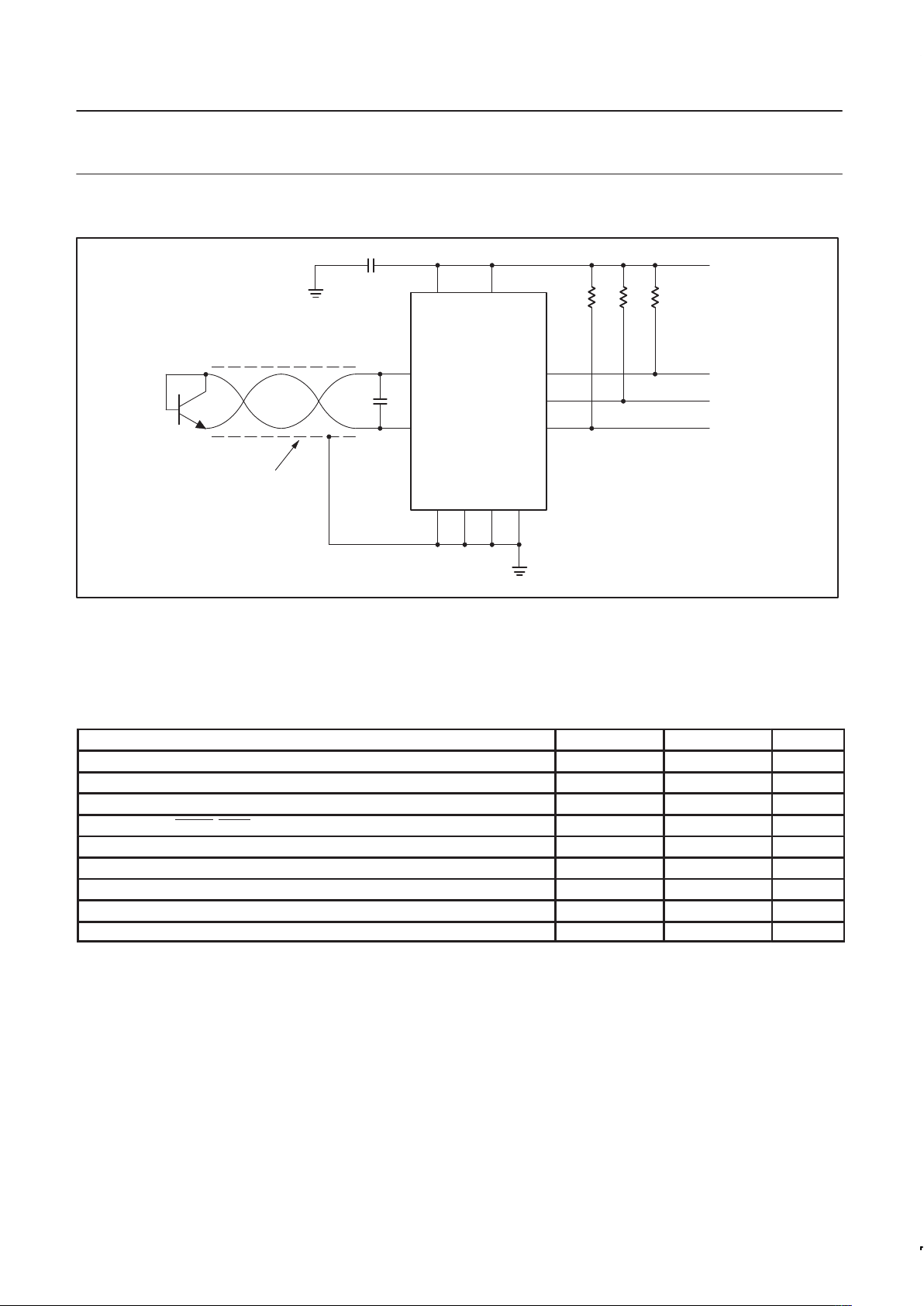
TYPICAL OPERATING CIRCUIT
215
14
12
11
10 6 7 8
SHIELDED
TWISTED PAIR
(NOTE 1)
REMOTE SENSOR
3
4
C
1
(NOTE 2)
0.1µF
V
DD
CLOCK
DATA
MICROCONTROLLER
INTERRUPT
10K10K10K
SL01203
NE1617
NOTES:
1. May be required if remote diode is in a noisy environment and/or several feet from the NE1617.
2. May be required in noisy environment. Up to 2200pF may be used.
Figure 2. Typical operating circuit
ABSOLUTE MAXIMUM RATINGS
PARAMETER MIN. MAX. UNIT
VDD to GND –0.3 +6 V
D+, ADD0, ADD1 –0.3 VDD+0.3 V
D– to GND –0.3 +0.8 V
SCLK, SDATA, ALERT, STBY –0.3 +6 V
Input current SDATA –1 +50 mA
D– current ±1 mA
Operating temperature range 0 +120 °C
Maximum junction temperature +150 °C
Storage temperature range –65 +150 °C
Page 5
Philips Semiconductors Product specification
NE1617Temperature monitor for microprocessor systems
1999 Mar 19
5
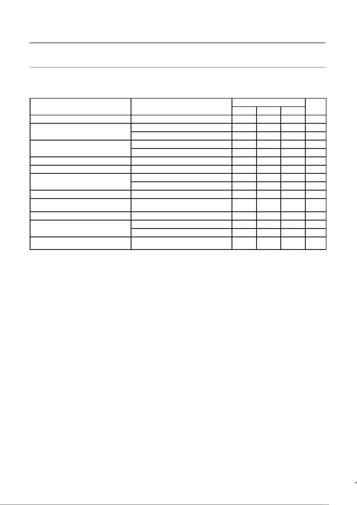
ELECTRICAL CHARACTERISTICS
VDD = 3.3V; T
amb
= 0°C to +125°C unless otherwise noted.
LIMITS
PARAMETER
CONDITIONS
MIN. TYP. MAX.
UNIT
T emperature resolution 1 °C
p
T
amb
= +60°C to +100°C < ±1 ±2 °C
Local temperature error
T
amb
= 0°C to +125°C < ±2 ±3 °C
p
T
remote
= +60°C to +100°C ±3 °C
Remote temperature error
T
remote
= 0°C to +125°C ±5 °C
Under voltage lockout VDD supply (Note 1) 2.0 2.95 V
Power-on reset threshold VDD supply (falling edge) (Note 2) 1.0 2.5 V
pp
Conversion rate = 0.25/sec 70 µA
Power supply current (average)
Conversion rate = 2/sec 180 µA
Power supply current (standby) SMBus inactive 3 10 µA
Conversion time
From stop bit to conversion complete,
both channels
170 ms
Conversion rate error Percentage error in programmed rate –30 +30 %
HIGH level 100 µA
Remote sensor source current
LOW level 10 µA
Address pin bias current
Momentary as the address is being read
(Notes 3 and 4)
160 µA
NOTES:
1. V
DD
(rising edge) voltage below which the ADC is disabled.
2. V
DD
(falling edge) voltage below which the logic is reset.
3. Address is read a power up and at start of conversion for all conversions except the fastest rate.
4. Due to the bias current, any pull-up/down resistors should be ≤ 2kΩ.
Page 6
Philips Semiconductors Product specification
NE1617Temperature monitor for microprocessor systems
1999 Mar 19
6
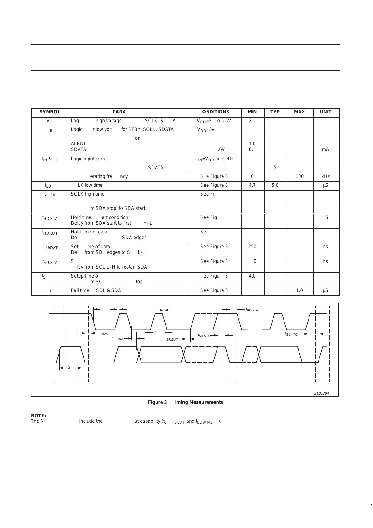
SMBUS INTERFACE AC SPECIFICATIONS
VDD = 3.0V to 3.6V; T
amb
= 0_C to +125_C unless otherwise noted.
These specifications are guaranteed by design and not tested in production.
SYMBOL
PARAMETER
CONDITIONS
MIN
TYP
MAX
UNIT
V
IH
Logic input high voltage for STBY, SCLK, SDATA
VDD=3V to 5.5V
2.2
V
V
IL
Logic input low voltage for STBY, SCLK, SDATA
VDD=3v to 5.5V
0.8
V
ÁÁÁ
Á
ÁÁÁ
Á
I
OL
ББББББББББББ
Á
ББББББББББББ
Á
Logic output low sink current for
ALERT
SDATA
ÁÁÁÁ
Á
ÁÁÁÁ
Á
VOL= 0.4V
V
O
L=0.6V
ÁÁ
Á
ÁÁ
Á
1.0
6.0
Á
Á
Á
Á
ÁÁ
Á
ÁÁ
Á
ÁÁ
Á
ÁÁ
Á
mA
mA
IIH & I
IL
Logic input current
VIN=VDD or GND
–1.0
1.0
µA
C
IN
SMBus input capacitance for SCLK,SDATA
5
pF
f
SCLK
SCLK operating frequency
See Figure 3
0
100
kHz
t
LOW
SCLK low time
See Figure 3
4.7
5.0
µS
t
HIGH
SCLK high time
See Figure 3
4.0
5.0
µS
ÁÁÁ
Á
t
BUF
ББББББББББББ
Á
SMBus free time.
Delay from SDA stop to SDA start
ÁÁÁÁ
Á
See Figure 3
ÁÁ
Á
4.7
ÁÁÁÁÁÁÁ
Á
µS
t
HD:STA
Hold time of start condition.
Delay from SDA start to first SCL H–L
See Figure 3
4.0
µS
ÁÁÁ
Á
t
HD:DAT
ББББББББББББ
Á
Hold time of data.
Delay from SCL H–L to SDA edges
ÁÁÁÁ
Á
See Figure 3
ÁÁ
Á
0
ÁÁÁÁÁÁÁ
Á
ns
ÁÁÁ
Á
t
SU:DAT
ББББББББББББ
Á
Setup time of data.
Delay from SDA edges to SCL L–H
ÁÁÁÁ
Á
See Figure 3
ÁÁ
Á
250
ÁÁÁÁÁÁÁ
Á
ns
t
SU:STA
Setup time of repeat start condition.
Delay from SCL L–H to restart SDA
See Figure 3
250
ns
ÁÁÁ
Á
t
SU:STO
ББББББББББББ
Á
Setup time of stop condition.
Delay from SCL L–H to SDA stop.
ÁÁÁÁ
Á
See Figure 3
ÁÁ
Á
4.0
ÁÁÁÁÁÁÁ
Á
µS
t
F
Fall time of SCL & SDA
See Figure 3
1.0
µS
t
BUF
P S
SCLK
SDATA
SL01204
t
HD:STA
SP
t
LOW
t
R t
F
t
HD:STA
t
HD:DAT
t
HIGH
t
SU:DAT
t
SU:STA
t
SU:STO
Figure 3. Timing Measurements
NOTE:
The NE1617 does not include the SMBUS timeout capability (t
LOW:SEXT
and t
LOW:MEXT
).
Page 7
Philips Semiconductors Product specification
NE1617Temperature monitor for microprocessor systems
1999 Mar 19
7
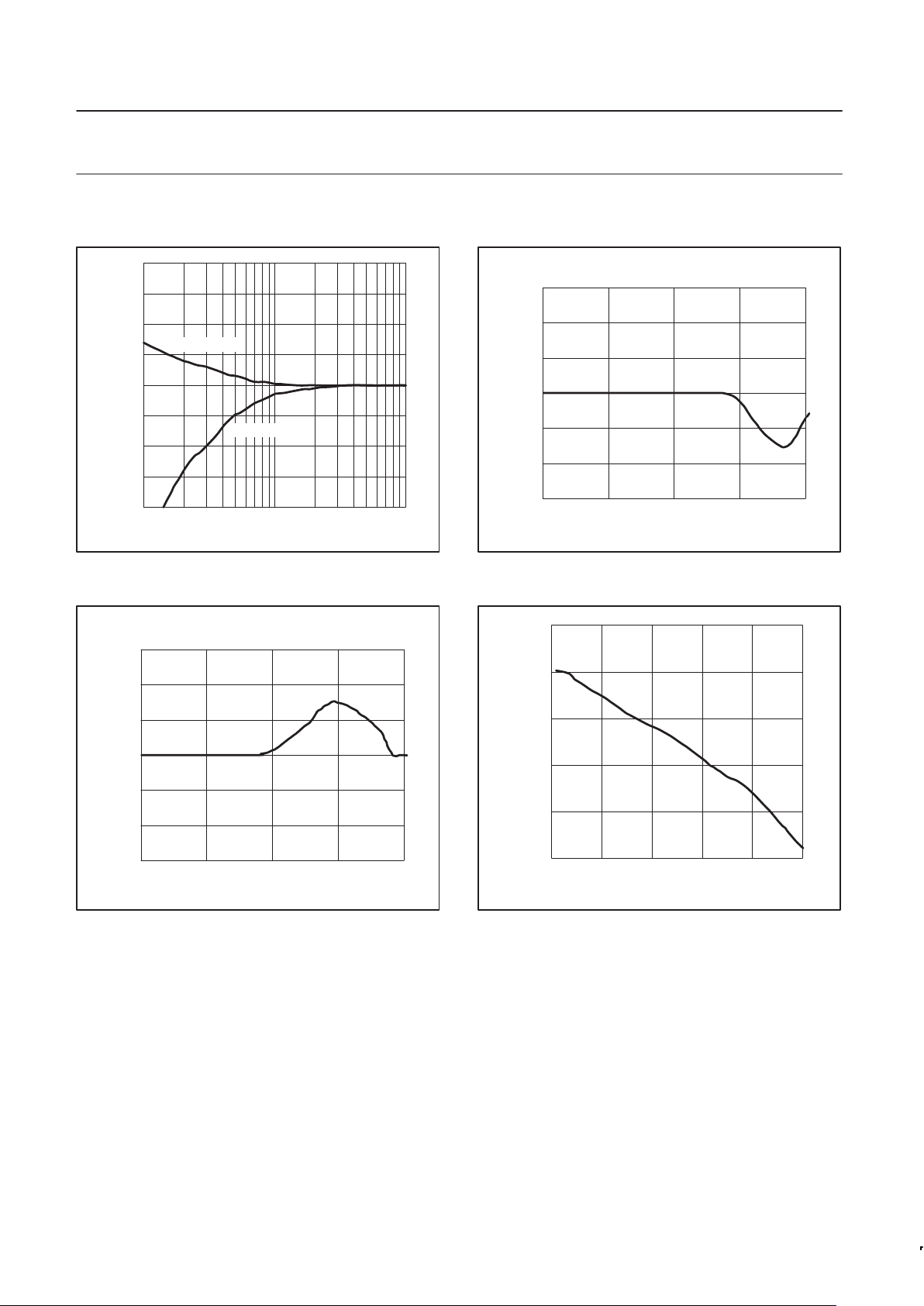
TYPICAL PERFORMANCE CHARACTERISTICS
LEAKAGE RESISTANCE (MΩ)
TEMPERATURE ERROR (deg. C)
1 10 100
20
15
10
5
0
–5
–10
–15
–20
D+ TO GND
D+ TO V
DD
SL01214
Figure 4. Temperature error vs. PC board resistance
VIN = 100mVPP and AC coupled to D–
1 10 100 1000 10000
6
4
2
0
–2
–4
–6
FREQUENCY (kHz)
TEMPERATURE ERROR (deg. C)
SL01212
Figure 5. Temperature error vs. common_mode noise
frequency
VIN = 100mVPP and AC coupled to D– and D+
FREQUENCY (kHz)
1 10 100 1000 10000
TEMPERATURE ERROR (deg. C)
6
4
2
0
–2
–4
–6
SL01211
Figure 6. Temperature error vs. differential mode noise
frequency
0 20406080100
5
0
–5
–10
–15
–20
D+ to D– CAPACITANCE (nF)
TEMPERATURE ERROR (deg. C)
SL01213
Figure 7. Temperature error vs. D+to D– capacitance
Page 8
Philips Semiconductors Product specification
NE1617Temperature monitor for microprocessor systems
1999 Mar 19
8
1 10 100 1000
SMB CLK FREQUENCY (kHz)
SUPPLY CURRENT (uA)
100
90
80
70
60
50
40
30
20
10
0
SL01217
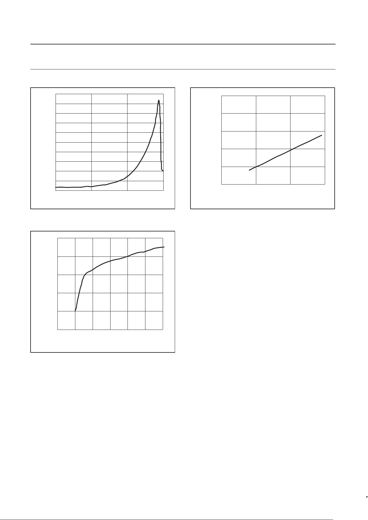
Figure 8. Standby supply current vs. clock frequency
@ V
CC
= 3.3 V
0.0625
0.125
0.25
0.5
1.0
2.0
4.0
8.0
CONVERSION RATE (Hz)
150
130
110
90
70
50
SUPPLY CURRENT (uA)
SL01216
Figure 9. Operating supply current vs. conversion rate
@ V
CC
= 3.3 V
–20246810
TIME (SEC)
125
100
75
50
25
0
TEMPERATURE (deg. C)
SL01215
Figure 10. Response to thermal shock immersed in +115°C
fluorinert bath
Page 9

Philips Semiconductors Product specification
NE1617Temperature monitor for microprocessor systems
1999 Mar 19
9
FUNCTIONAL DESCRIPTION
The NE1617 contains an integrating A-to-D converter, an analog
multiplexer, a status register, digital data registers, SMBUS
interface, associated control logic and a local temperature sensor or
channel. The remote diode-type sensor or channel should be
connected to the D+ and D– pins properly.
Temperature measurements or conversions are either automatically
and periodically activated when the device is in free-running mode
(both STBY
pin = high, and the configuration register BIT6 = low) or
generated by one-shot command. The free-running period is selected
by changing the programmable data of the conversion rate register
as described later. For each conversion, the multiplexer switches
current sources through the remote and local temperature sensors
over a period of time, about 60ms, and the voltages across the
diode-type sensors are sensed and converted into the temperature
data by the A-to-D converter. The resulting temperature data is then
stored in the temperature registers, in 8-bit, two’s complement word
format and automatically compared with the limits which have been
programmed in the temperature limit registers. Results of the
comparison are reflected accordingly by the flags stored in the
status register, an out-of-limit condition will set the ALERT
output pin
to its low state. Because both channels are automatically measured
for each conversion, the results are updated for both channels at the
end of every successful conversion.
Remote diode selection
The method of the temperature measurement is based on the
change of the diode VBE at two different operating current levels
given by:
DVBE +
KT
q
< LN(N)
where:
K: Boltzman’s constant
T: absolute temperature in ° Kelvin
q: charge on the electron
N: ratio of the two currents
LN: natural logarithm
The NE1617 provides two current sources of about 10µA and 100µA
in measuring the remote diode VBE and the sensed voltage
between two pins D+ and D– is limited between 0.25V and 0.95V .
The external diode must be selected to meet this voltage range at
these two current levels. The diode-connected PNP transistor
provided on the microprocessor is typically used, or the discrete
diode-connected transistor 2N3904 is recommended as an
alternative.
Even though the NE1617 integrating A-to-D converter has a good
noise performance, using the average of 10 measurement cycles,
high frequency noise filtering between D+ and D– should be
considered. An external capacitor of 2200pF typical (but not higher
than 3300pF) connected between D+ and D– is recommended.
Capacitance higher than 3300pF will introduce measurement error
due to the rise time of the switched current source.
Address logic
The address pins of the NE1617 can be forced into one of three
levels: Low (GND), High (V
DD
), or not connected (NC). Because the
NE1617 samples and latches the address pins at the starting of
every conversion, it is suggested that those address pins should be
hardwired to the logic applied, so that the logic is consistently
existed at the address pins. During the address sensing period, the
device forces a current at each address pin and compares the
voltage developed across the external connection with the
predefined threshold voltage in order to define the logic level. If an
external resistor is used for the connection of the address, then its
value should be less than 2kΩ to prevent the error in logic detection
from happening. Resistors of 1kΩ is recommended.
Page 10
Philips Semiconductors Product specification
NE1617Temperature monitor for microprocessor systems
1999 Mar 19
10
TEMPERATURE MONITOR WITH SMB SERIAL
INTERFACE
Serial bus interface
The device can be connected to a standard 2-wire serial interface
System Management Bus (SMBus) as a slave device under the
control of a master device, using two device terminals SCLK and
SDATA. The operation of the device to the bus is described with
details in the following sections.
Slave address
The device address is defined by the logical connections applied to
the device pins ADD0 and ADD1. A list of selectable addresses are
shown in Table 1. The device address can be set to any one of
those nine combinations and more than one device can reside on
the same bus without address confliction. Note that the state of the
device address pins is sampled and latched not only at power-up
step but also at starting point of every conversion.
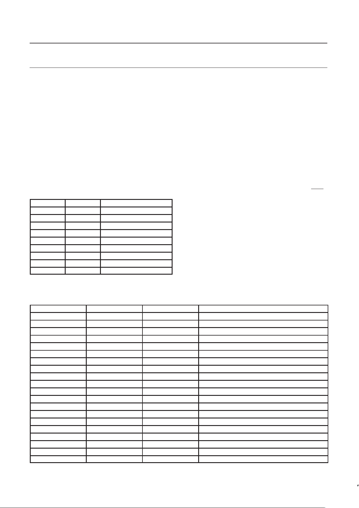
Table 1. Device slave address
ADD0* ADD1* ADDRESS BYTE
GND GND 0011 000
GND NC 0011 001
GND V
DD
0011 010
NC GND 0101 001
NC NC 0101 010
NC V
DD
0101 011
V
DD
GND 1001 100
V
DD
NC 1001 101
V
DD
V
DD
1001 110
NC = Not Connected.
* Any pull-up/down resistor used to connect to GND or V
DD
should
be ≤ 2kΩ.
Registers
The device contains more than 9 registers. They are used to store
the data of device setup and operation results. Depending on the
bus communication (either read or write operations), each register
may be called by different names because each register may have
different sub-addresses or commands for read and write operations.
For example, the configuration register is called as WC for write
mode and as RC for read mode. Table 2 (Register Assignments)
shows the names, commands and functions of all registers as well
the register POR states.
Note that attempting to write to a read-command or read from a
write-command will produce an invalid result. The reserved registers
are used for factory test purposes and should not be written to.
Low power standby modes
Upon POR, the device is reset to its normal free-running
auto-conversion operation mode. The device can be put into
standby mode by either using hardware control (connect the STBY
pin to LOW for hardware standby mode) or using software control
(set bit 6 of the configuration register to HIGH for software standby
mode). When the device is put in either one of the standby modes,
the supply current is reduced to less than 10µA if there is no SMBus
activity, all data in the device registers are retained and the SMBus
interface is still alive to bus communication. However, there is a
difference in the device ADC conversion operation between
hardware standby and software standby modes. In hardware
standby mode, the device conversion is inhibited and the one-shot
command does not initiate a conversion. In software standby mode,
the one-shot command will initiate a conversion for both internal and
external channels.
If a hardware standby command is received when the device is in
normal mode and a conversion is in progress, the conversion cycle
will stop and data in reading temperature registers will not be
updated.
Table 2. Register assignments
REGISTER NAME COMMAND BYTE POR STATE FUNCTION
RIT 00h 0000 0000 Read internal or local temp byte
RET 01h 0000 0000 Read external or remote temp byte
RS 02h n/a Read status byte
RC 03h 0000 0000 Read configuration byte
RCR 04h 0000 0010 Read conversion rate byte
RIHL 05h 0111 1111 Read internal temp HIGH limit byte
RILL 06h 1100 1001 Read internal tem low limit byte
REHL 07h 0111 1111 Read external temp HIGH limit byte
RELL 08h 1100 1001 Read external temp LOW limit byte
WC 09h n/a Write configuration byte
WCR 0Ah n/a Write conversion rate byte
WIHL 0Bh n/a Write internal temp HIGH limit byte
WILL 0Ch n/a Write internal temp LOW limit byte
WEHL 0Dh n/a Write external temp HIGH limit byte
WELL 0Eh n/a Write external temp LOW limit byte
OSHT 0Fh n/a One shot command
RESERVED 10h n/a Reserved
RESERVED 11h n/a Reserved
RESERVED 12h n/a Reserved
RESERVED 13h n/a Reserved
Page 11
Philips Semiconductors Product specification
NE1617Temperature monitor for microprocessor systems
1999 Mar 19
11
Configuration register
The configuration register is used to mask the Alert interrupt and/or
to put the device in software standby mode. Only two bits 6 and 7 of
this register are used as listed in Table 3. Bit 7 is used to mask the
device ALERT
output from Alert interruption when this bit is set to 1
and bit 6 is used to activate the standby software mode when this bit
is set to to 1.
This register can be written or read using the commands of registers
named WC and RC accordingly. Upon power-on reset (POR), both
bits are reset to zero.
Table 3. Configuration register bit assignments
BIT NAME
POR
STATE
FUNCTION
7 (MSB) MASK 0 Mask ALERT interrupt:
Interrupt is enabled when
this bit is LOW, and disabled
when this bit is HIGH.
6 RUN/STOP 0 Standby or run mode
control:
When LOW, running mode is
enabled. When HIGH,
standby mode is initiated.
5 to 0 RESERVED n/a n/a
External and internal temperature registers
Results of temperature measurements after every ADC conversion
are stored in two registers: Internal Temp register (RIT) for internal
or local diode temperature, and External Temp register (RET) for
external or remote diode temperature. These registers can be only
read over the SMBus. The reading temperature data is in 2’s
complement binary form consisting of 7-bit data and 1-bit sign
(MSB), with each data count represents 1°C, and the MSB bit is
transmitted first over the serial bus. The contents of those two
registers are updated upon completion of each ADC conversion.
Table 4 shows some values of the temperature and data.
Table 4. Temperature data format
(2’s complement)
TEMPERATURE (°C) DIGITAL OUTPUT (8 BITS)
+127 0 111 1111
+126 0 111 1110
+100 0 110 0100
+50 0 011 0010
+25 0 001 1001
+1 0 000 0001
0 0 000 0000
–1 1 111 1111
–25 1 110 0111
–50 1 100 1110
–65 1 011 1111
Conversion rate register
The conversion rate register is used to store programmable
conversion data, which defines the time interval between
conversions in standard free-running auto-convert mode. The
Table 5 shows all applicable data and rates for the device. Only
three LSB bits of the register are used and other bits are reserved
for future use. This register can be written to and read back over the
SMBus using commands of the registers named WCR and RCR
respectively. The POR default conversion data is 02h (0.25Hz).
Notice that the average supply current, as well as the device power
consumption, is increased with the conversion rate.
Table 5. Conversion rate control byte
DATA CONVERSION
RATE (Hz)
AVERAGE
SUPPLY CURRENT
(µA Typ. @ V
DD
= 3.3V)
00h 0.0625 TBD
01h 0.125 TBD
02h 0.25 TBD
03h 0.5 TBD
04h 1 TBD
05h 2 TBD
06h 4 TBD
07h 8 TBD
08h to FFh Reserved n/a
T emperature limit registers
The device has four registers to be used for storing programmable
temperature limits, including the high limit and the low limit for each
channel of the external and internal diodes. Data of the temperature
register (RIT & RET) for each channel are compared with the
contents of the temperature limit registers of the same channel,
resulting in alarm conditions. If measured temperature either equals
or exceeds the corresponding temperature limits, an Alert interrupt is
asserted and the corresponding flag bit in the status register is set.
The temperature limit registers can be written to and read back
using commands of registers named WIHL, WILL, WEHL, WELL,
RIHL, RILL, REHL, RELL accordingly. The POR default values are
+127°C (01 11 1 111) for the HIGH limit and –55°C (1100 1001) for the
LOW limit.
One-shot command
The one shot command is not actually a data register as such and a
write operation to it will initiate an ADC conversion. The send byte
format of the SMBus, as described later, with the use of OSHT
command (0Fh), is used for this writing operation. In normal
free-running-conversion operation mode of the device, a one-shot
command immediately forces a new conversion cycle to begin.
However, if a conversion is in progress when a one-shot command
is received, the command is ignored. In software standby mode, the
one-shot command generates a single conversion and comparison
cycle and then puts the device back in its standby mode after the
conversion. In hardware standby mode, the one shot is inhibited.
Page 12

Philips Semiconductors Product specification
NE1617Temperature monitor for microprocessor systems
1999 Mar 19
12
Status register
The content of the status register reflects condition status resulting
from all of these activities: comparisons between temperature
measurements and temperature limits, the status of ADC
conversion, and the hardware condition of the connection of external
diode to the device. Bit assignments and bit functions of this register
are listed in Table 6. This register can only be read using the
command of register named RS. Upon POR, the status of all flag
bits are reset to zero. The status byte is cleared by any successful
read of the status register unless the fault condition persists.
Notice that any one of the fault-conditions, except the conversion
busy, also introduces an Alert interrupt to the SMBus that will be
described in the following section. Also, whenever a one-shot
command is executed, the status byte should be read after the
conversion is completed, which is about 170ms after the one-shot
command is sent.
Table 6. Status register bit assignment
BIT NAME
POR
STATE
FUNCTION
7 (MSB) BUSY n/a High when the ADC is busy
converting
6 IHLF* 0 High when the internal
temperature high limit has tripped
5 ILLF* 0 High when the internal
temperature low limit has tripped
4 EHLF* 0 High when the external
temperature high limit has tripped
3 ELLF* 0 High when the external
temperature low limit has tripped
2 OPEN* 0 High when the external diode is
opened
1 to 0 n/a 0 Reserved
* These flags stay high until the status register is read or POR is
activated.
Alert interrupt
The ALERT output is used to signal Alert interruption from the
device to the SMBus and is active low. Because this output is an
open-drain output, a pull-up resistor (10kΩ typ) to V
DD
is required,
and slave devices can share a common interrupt line on the same
SMBus. An Alert interrupt is asserted by the device whenever any
one of the fault conditions, as described in the Status register
section, occurs: measured temperature equals or exceeds
corresponding temp limits, the remote diode is physically
disconnected from the device pins. Alert interrupt signal is latched
and can only be cleared by reading the Alert Response byte from
the Alert Response Address which is a special slave address to the
SMBus. The ALERT
output can not be reset by reading the device
status register. The device was designed to accommodate the Alert
interrupt detection capability of the SMBus.
Basically, the SMBus provides Alert response interrupt pointers in
order to identify the slave device which has caused the Alert
interrupt. The 7-bit Alert response slave address is 0001 100 and
the Alert response byte reflects the slave address of the device
which has caused Alert interrupt. Bit assignments of the Alert
response byte are listed in Table 7. The ALERT
output will be reset
to HIGH state upon reading the Alert response slave address unless
the fault condition persists.
Table 7. Alert response bit assignment
(Alert response address = 0001 100)
ALERT
RESPONSE
BIT
NAME
ADDRESS
BIT
FUNCTION
7 (MSB) ADD7 Indicate address B6 of alerted device
6 ADD6 Indicate address B5 of alerted device
5 ADD5 Indicate address B4 of alerted device
4 ADD4 Indicate address B3 of alerted device
3 ADD3 Indicate address B2 of alerted device
2 ADD2 Indicate address B1 of alerted device
1 ADD1 Indicate address B0 of alerted device
0 (LSB) 1 Logic 1
Page 13

Philips Semiconductors Product specification
NE1617Temperature monitor for microprocessor systems
1999 Mar 19
13
Power-up default condition
Upon power-up reset (power is switched off-on), the NE1617 goes
into this default condition:
– Interrupt latch is cleared, the ALERT
output is pulled high by the
external pull-up resistor.
– The auto-conversion rate is at 0.25Hz; conversion rate data is
02H.
– Temperature limits for both channels are +127°C for high limit, and
–55°C for low limit.
– Command pointer register is set to 00 for quickly reading the RIT.
Fault detection
The NE1617 has a fault detector to the diode connection. The
connection is checked when a conversion is initiated and the proper
flags are set if the fault condition has occurred.
D+ & D–
ALERT
OUTPUT
RET DATA
STORAGE
STATUS SET
FLAG
Opened Low 127°C B2 & B4
Shorted Low 127°C B4
SMBus interface
The device can communicate over a standard 2-wire serial interface
System Management Bus (SMBus) using the device pins SCLK and
SDATA. The device employs four standard SMBus protocols: Write
Byte, Read Byte, Send Byte and Receive Byte. Data formats of
those protocols are shown in Table 8 with following notifications:
– The SMBus master initiates data transfer by establishing a start
condition (S) and terminates data transfer by generating a stop
condition (P).
– Data is sent over the serial bus in sequence of 9 clock pulses
according to each 8-bit data byte followed by 1-bit status of the
device acknowledgement.
– The 7-bit slave address is equivalent to the selected address of
the device.
– The command byte is equivalent to the selected command of the
device register
– The send byte format is often used for the one-shot conversion
command.
– The receive byte format is used for quicker transfer data from a
device reading register which was previously selected by a read
byte format.
T able 8. SMBus programming format
Write byte format (for writing data byte to the device register):
S
ADDRESS WR ACK COMMAND ACK DATA ACK P
7 bits
device address
1 bit = 0 by
device
8 bits
device registerbydevice
8 bits
to register
by
device
Read byte format (for reading data byte from the device register):
S
ADDRESS WR ACK COMMAND ACK S ADDRESS RD ACK DATA NACK P
7 bits
device address
1 bit = 0 by
device
8 bits
device register
by
device
7 bits
device address
1 bit = 1 by
device
8 bits
from
register
by
controller
Send byte format (for sending command without data, such as one–shot command):
S
ADDRESS WR ACK COMMAND ACK P
7 bits
device address
1 bit = 0 by
device
8 bits
device register
by
device
Receive byte format (for continuously reading from device register):
S
ADDRESS RD ACK DATA NACK P
7 bits
device address
1 bit = 1 by
device
8 bits
from register
by
controller
NOTES:
S = Start condition
P = Stop condition
ACK = Acknowledged
NACK = Not acknowledged
Page 14

Philips Semiconductors Product specification
NE1617Temperature monitor for microprocessor systems
1999 Mar 19
14
PC BOARD LAYOUT CONSIDERATION
Because the NE1617 is used to measure a very small voltage from
the remote sensor, care must be taken to minimize noise induced at
the sensor inputs, especially in the computer motherboard noisy
environment. These precautions should be considered:
– Place the NE1617 as close as possible to the remote sensor. It
can be from 4 to 8 inches, as long as the worst noise sources
such as clock generator, data and address buses, CRTs are
avoided.
– Route the D+ and D– lines in parallel and close together with
ground guards enclosed.
– Leakage currents due to PC board contamination must be
considered. Error can be introduced by the leakage current as
shown on the characteristics curve (Temperature Error vs. PC
Board Resistance).
– Use wide tracks to reduce inductance and noise pickup that may
be introduced by narrow ones. The width of 10 mil and space of
10 mil are recommended.
GND
D+
D–
GND
SL01218
– Place a bypass capacitor of 0.1µF close to the VDD pin and an
input filter capacitor of 2200pF close to the D+ and D– pins.
– A shielded twisted pair is recommended for a long distance
remote sensor. Connect the shield of the cable at the device side
to the NE1617 GND pin and leave the shield at the remote end
unconnected to avoid ground loop. Also notice that the series
resistance of the cable may introduce measurement error; 1Ω can
introduce about 0.5°C.
Page 15
Philips Semiconductors Product specification
NE1617Temperature monitor for microprocessor systems
1999 Mar 19
15
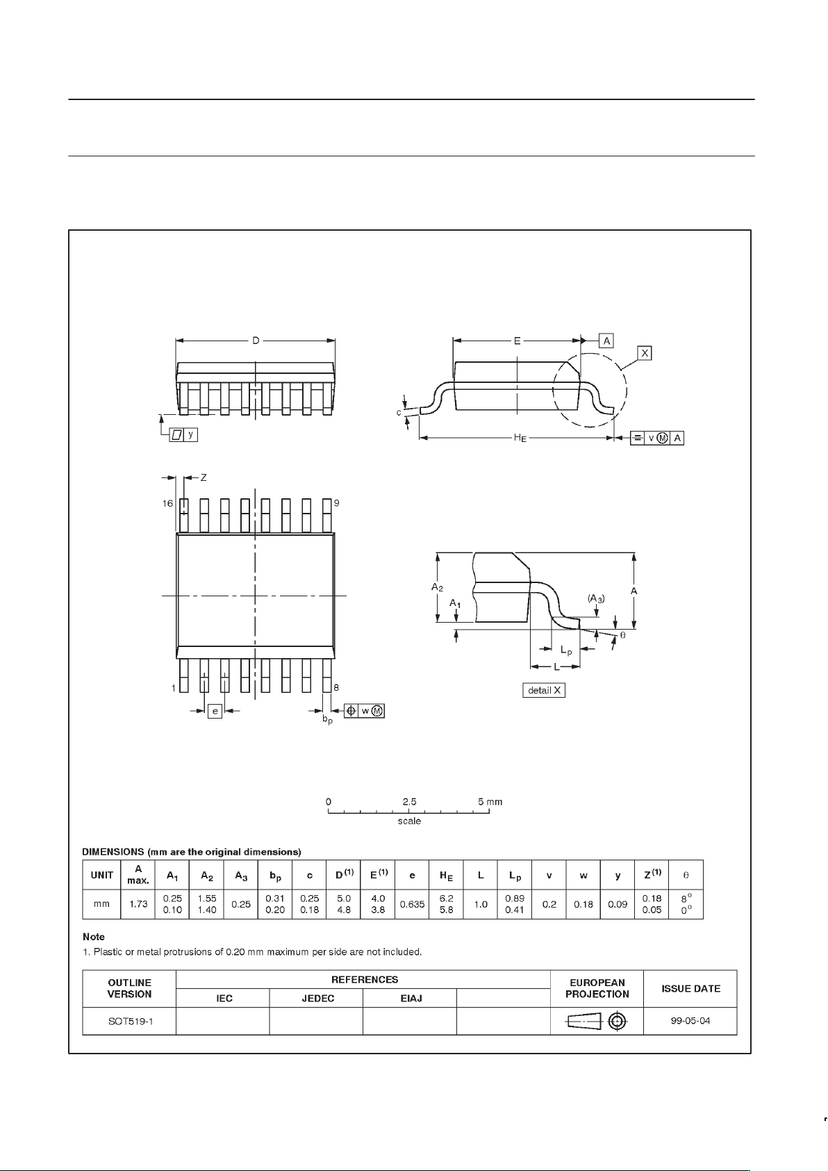
SSOP16: plastic shrink small outline package; 16 leads; body width 3.9 mm;
lead pitch 0.635 mm SOT519-1
Page 16

Philips Semiconductors Product specification
NE1617Temperature monitor for microprocessor systems
1999 Mar 19
16
Definitions
Short-form specification — The data in a short-form specification is extracted from a full data sheet with the same type number and title. For
detailed information see the relevant data sheet or data handbook.
Limiting values definition — Limiting values given are in accordance with the Absolute Maximum Rating System (IEC 134). Stress above one
or more of the limiting values may cause permanent damage to the device. These are stress ratings only and operation of the device at these or
at any other conditions above those given in the Characteristics sections of the specification is not implied. Exposure to limiting values for extended
periods may affect device reliability.
Application information — Applications that are described herein for any of these products are for illustrative purposes only. Philips
Semiconductors make no representation or warranty that such applications will be suitable for the specified use without further testing or
modification.
Disclaimers
Life support — These products are not designed for use in life support appliances, devices or systems where malfunction of these products can
reasonably be expected to result in personal injury . Philips Semiconductors customers using or selling these products for use in such applications
do so at their own risk and agree to fully indemnify Philips Semiconductors for any damages resulting from such application.
Right to make changes — Philips Semiconductors reserves the right to make changes, without notice, in the products, including circuits, standard
cells, and/or software, described or contained herein in order to improve design and/or performance. Philips Semiconductors assumes no
responsibility or liability for the use of any of these products, conveys no license or title under any patent, copyright, or mask work right to these
products, and makes no representations or warranties that these products are free from patent, copyright, or mask work right infringement, unless
otherwise specified.
Philips Semiconductors
811 East Arques Avenue
P.O. Box 3409
Sunnyvale, California 94088–3409
Telephone 800-234-7381
Copyright Philips Electronics North America Corporation 1999
All rights reserved. Printed in U.S.A.
Date of release: 08-99
Document order number: 9397 750 06385
Data sheet
status
Objective
specification
Preliminary
specification
Product
specification
Product
status
Development
Qualification
Production
Definition
[1]
This data sheet contains the design target or goal specifications for product development.
Specification may change in any manner without notice.
This data sheet contains preliminary data, and supplementary data will be published at a later date.
Philips Semiconductors reserves the right to make chages at any time without notice in order to
improve design and supply the best possible product.
This data sheet contains final specifications. Philips Semiconductors reserves the right to make
changes at any time without notice in order to improve design and supply the best possible product.
Data sheet status
[1] Please consult the most recently issued datasheet before initiating or completing a design.
 Loading...