

Page 1
© Semiconductor Components Industries, LLC, 2011
December, 2011 − Rev. P1
1 Publication Order Number:
EVBUM2050/D
NCV890201GEVB
NCV890201 Automotive
Grade High-Frequency
Buck Regulator Evaluation
Board User's Manual
Description
The NCV890201 demonstration board provides a convenient way to
evaluate a high-frequency buck converter design. No additional
components are required, other than dc supplies for the input and
enable voltages. An external clock can be used to synchronize the
switching frequency; and the board also provides a synchronization
output, enabling it to be used as a master. It is configured for a 3.3 V
output with a 2 MHz switching frequency and a 2.0 A maximum
output current, over the typical 4.5 V to 18 V automotive input voltage
range. In addition, the board regulates up to 36 V thanks to switching
frequency foldback.
Key Features
• 3.3 V Output Voltage
• 2 MHz Switching Frequency
• 2.0 A Current Limit
• Wide Input Voltage of 4.5 V to 36 V
• Regulates through Load Dump Conditions
• External Clock Synchronization up to 2.5 MHz
• Synchronization Output
• Automotive Grade
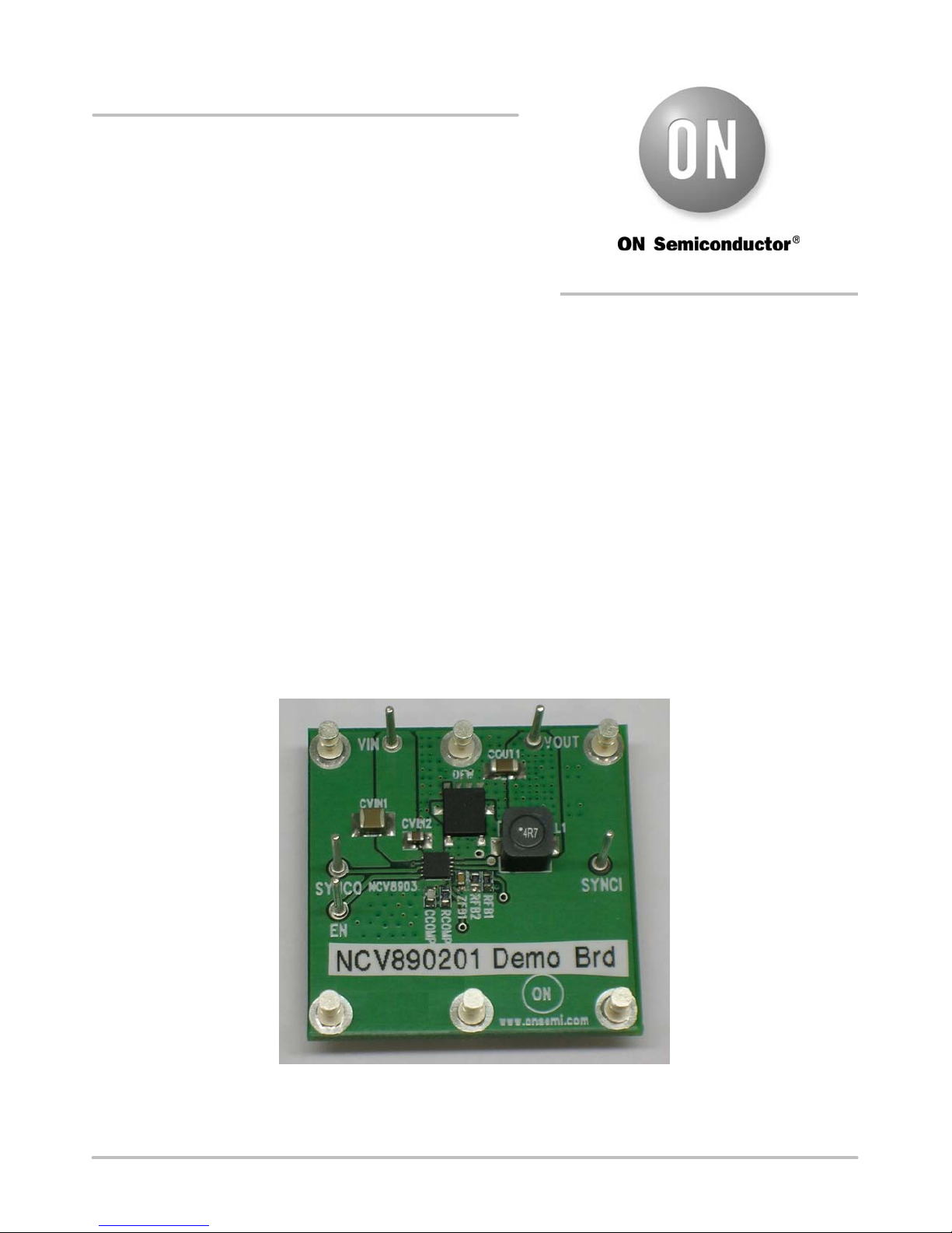
Figure 1. NCV890201GEVB Board Picture
http://onsemi.com
EVAL BOARD USER’S MANUAL
Page 2
NCV890201GEVB
http://onsemi.com
2
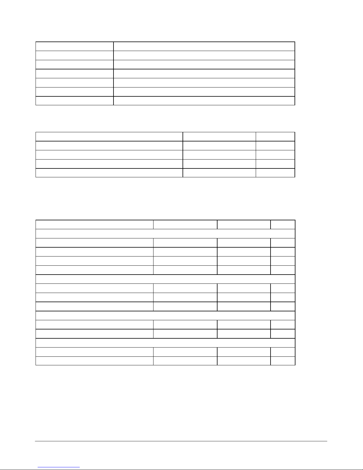
Table 1. DEMONSTRATION BOARD TERMINALS
Terminal Function
VIN Positive dc input voltage
GND Common dc return
VOUT Regulated dc output voltage
EN Enable input
SYNCI Input for external clock synchronization
SYNCO Output for synchronizing other boards
Table 2. ABSOLUTE MAXIMUM RATINGS
(Voltages are with respect to GND)
Rating
Value Units
Dc supply voltage (VIN, EN) -0.3 to 36 V V
Dc supply voltage (SYNCI) -0.3 to 6 V V
Junction Temperature (NCV890201) -40 to 150 °C
Ambient temperature (Demo Board) -40 to 85 °C
Stresses exceeding Maximum Ratings may damage the device. Maximum Ratings are stress ratings only. Functional operation
above the Recommended Operating Conditions is not implied. Extended exposure to stresses above the Recommended
Operating Conditions may affect device reliability.
Table 3. ELECTRICAL CHARACTERISTICS
(TA = 25°C, 4.5 V ≤ VIN ≤ 40 V, VEN = 2 V, V
OUT
= 3.3 V, 0 ≤ I
OUT
≤ 2.0 A, unless otherwise specified)
Characteristics
Conditions Typical Value Units
Regulation
Output Voltage 3.30 V
Voltage Accuracy 4 %
Line Regulation I
OUT
= 1.0 A 0.12 %
Load Regulation VIN = 13.2 V 0.03 %
Switching
Switching Frequency 2.0 MHz
Soft-start Time 1.4 ms
SYNCI Frequency range 1.8 to 2.5 MHz
Current Limit
Average Current Limit VIN = 6 to 18 V 1.8 A
Cycle-by-cycle Current Limit 2.45 A
Protections
Input Undervoltage Lockout (UVLO) VIN decreasing 4.2 V
Thermal Shutdown TA increasing 170 °C
Page 3

NCV890201GEVB
http://onsemi.com
3
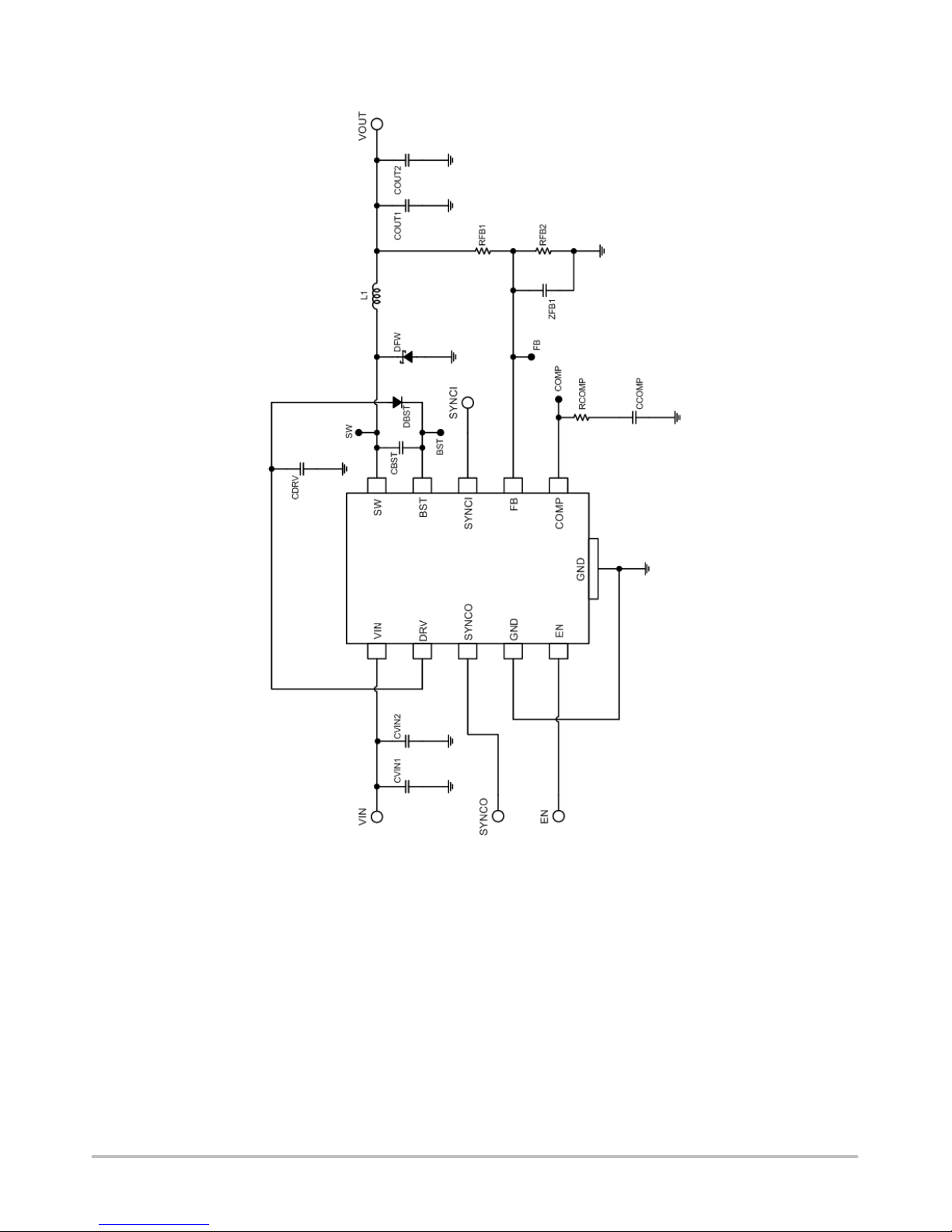
Figure 2. NCV890201GEVB Board Schematic
Operational Guidelines
1. Connect a dc input voltage, within the 4.5 V to 36 V range, between VIN and GND
2. Connect a load between VOUT and GND
3. Connect a dc enable voltage, within the 4.5 V to 36 V range, between EN and GND
4. Optionally, for external clock synchronization, connect a pulse source between SYNCI and GND. The high state level
should be within the 2 to 6 V range, and the low state level within the -0.3 V to 0.8 V range, with a minimum pulse
width of 40 ns and a frequency within the 1.8 to 2.5 MHz range.
Figure 3. NCV890201GEVB Board Connections
V
IN
V
EN
Z
OUT
V
SYNCI
I
OUT
Page 4
NCV890201GEVB
http://onsemi.com
4
TYPICAL PERFORMANCE
Efficiency
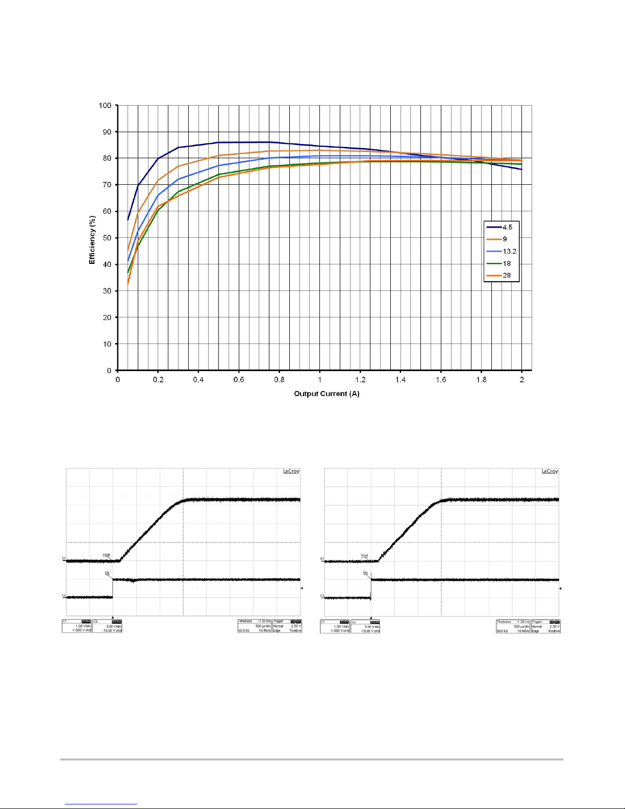
Figure 4. Efficiency at 2 MHz for a 3.3 V output
Start−up
Figure 5. Typical start−up with V
IN
= 13.2 V,
V
OUT
= 3.3 V and I
OUT
= 0.2 A
Figure 6. Typical start−up with V
IN
= 13.2 V,
V
OUT
= 3.3 V and I
OUT
= 1.8 A
Page 5
NCV890201GEVB
http://onsemi.com
5
Load Transients
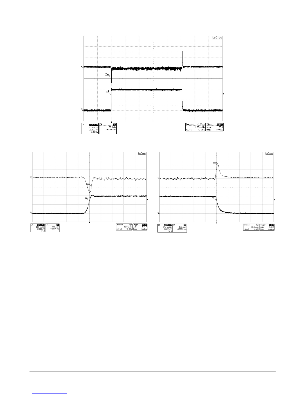
Figure 7. Load transient 0.1 A to 2.0 A,
with V
OUT
= 3.3 V and VIN = 13.2 V
Figure 8. Load transient 0.2 A to 2.0 A,
with V
OUT
= 3.3 V and VIN = 13.2 V
Figure 9. Load transient 2.0 A to 0.2 A,
with V
OUT
= 3.3 V and VIN = 13.2 V
Page 6
NCV890201GEVB
http://onsemi.com
6
Synchronization
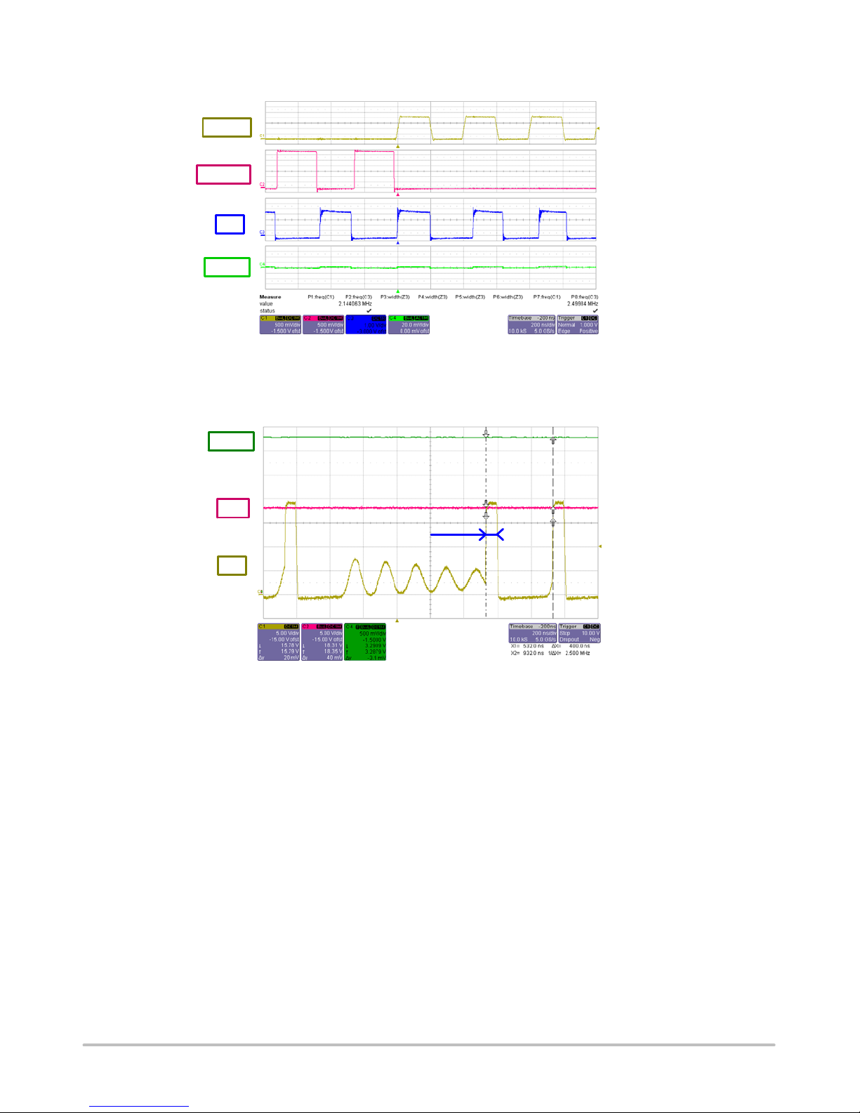
Figure 10. Starting synchronization at 2.5 MHz (from free−running)
SYNCI
SYNCO
SW
VOUT
Minimum on time
Figure 11. Minimum on time seen during a load transient
VIN
SW
VOUT
80 ns
Page 7
NCV890201GEVB
http://onsemi.com
7
Schematic
Page 8
NCV890201GEVB
http://onsemi.com
8
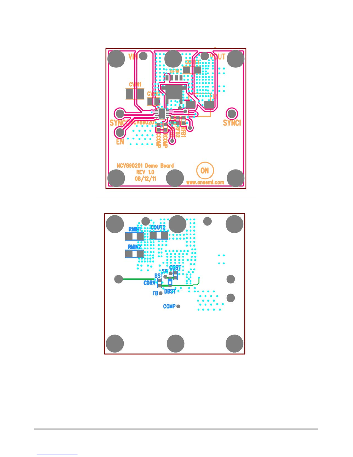
PCB LAYOUT
Figure 12. Top View
Figure 13. Bottom View
Page 9
NCV890201GEVB
http://onsemi.com
9
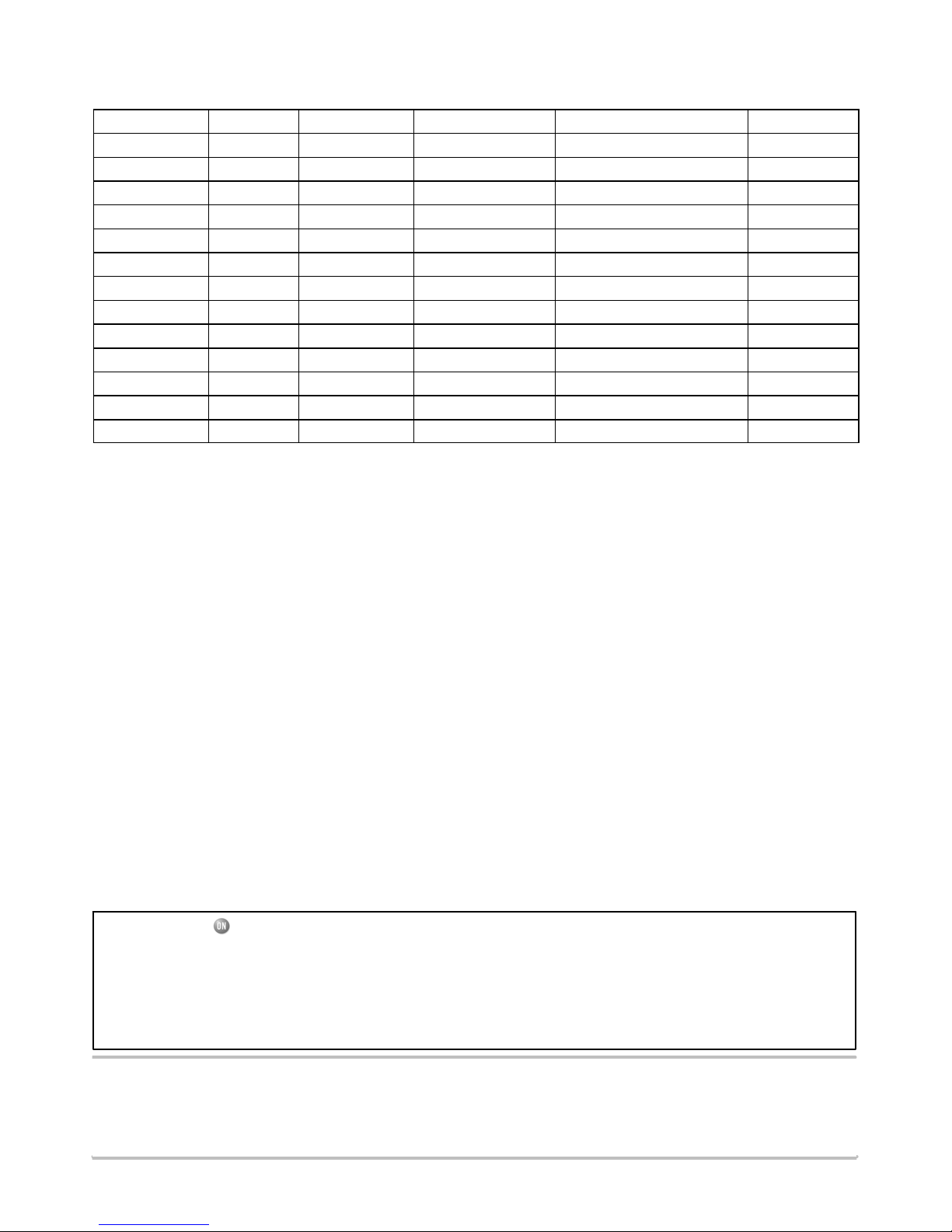
Table 4. BILL OF MATERIALS
Reference Value Part # Manufacturer Description Package
U1 NCV890201 ON Semiconductor Integrated circuit 3x3 DFN10
L1
4.7 mH
7447786004 Wurth Inductor WE-PD-XS
DFW MBR340MFS ON Semiconductor Diode, Schottky, 1.5A, 40V SMB
DBST BAS16HT1 ON Semiconductor Diode, Switching, 200mA, 75V SOD-323
CVIN1
4.7 mF
Murata Capacitor, Ceramic, 50V, X7R 1210
CVIN2
1 mF
Murata Capacitor, Ceramic, 50V, X5R 0805
CDRV, CBST
0.1 mF
Kemet Capacitor, Ceramic, 10V, X7R 0603
ZFB1 4.7 nF Murata Capacitor, Ceramic, 50V, X7R 0603
COUT1, COUT2
10 mF
Murata Capacitor, Ceramic, 10V, X7R 1206
CCOMP 330 pF Murata Capacitor, Ceramic, 50V, C0G 0603
RCOMP
12.4 KW
Vishay Resistor, 1% 0603
RFB1
100 W
Vishay Resistor, 1% 0603
RFB2
31.6 W
Vishay Resistor, 1% 0603
ON Semiconductor and are registered trademarks of Semiconductor Components Industries, LLC (SCILLC). SCILLC reserves the right to make changes without further notice
to any products herein. SCILLC makes no warranty, representation or guarantee regarding the suitability of its products for any particular purpose, nor does SCILLC assume any liability
arising out of the application or use of any product or circuit, and specifically disclaims any and all liability, including without limitation special, consequential or incidental damages.
“Typical” parameters which may be provided in SCILLC data sheets and/or specifications can and do vary in different applications and actual performance may vary over time. All
operating parameters, including “Typicals” must be validated for each customer application by customer’s technical experts. SCILLC does not convey any license under its patent rights
nor the rights of others. SCILLC products are not designed, intended, or authorized for use as components in systems intended for surgical implant into the body, or other applications
intended to support or sustain life, or for any other application in which the failure of the SCILLC product could create a situation where personal injury or death may occur. Should
Buyer purchase or use SCILLC products for any such unintended or unauthorized application, Buyer shall indemnify and hold SCILLC and its officers, employees, subsidiaries, affiliates,
and distributors harmless against all claims, costs, damages, and expenses, and reasonable attorney fees arising out of, directly or indirectly, any claim of personal injury or death
associated with such unintended or unauthorized use, even if such claim alleges that SCILLC was negligent regarding the design or manufacture of the part. SCILLC is an Equal
Opportunity/Affirmative Action Employer. This literature is subject to all applicable copyright laws and is not for resale in any manner.
PUBLICATION ORDERING INFORMATION
N. American Technical Support: 800−282−9855 Toll Free
USA/Canada
Europe, Middle East and Africa Technical Support:
Phone: 421 33 790 2910
Japan Customer Focus Center
Phone: 81−3−5817−1050
EVBUM2050/D
LITERATURE FULFILLMENT:
Literature Distribution Center for ON Semiconductor
P.O. Box 5163, Denver, Colorado 80217 USA
Phone: 303−675−2175 or 800−344−3860 Toll Free USA/Canada
Fax: 303−675−2176 or 800−344−3867 Toll Free USA/Canada
Email: [email protected]
ON Semiconductor Website: www.onsemi.com
Order Literature: http://www.onsemi.com/orderlit
For additional information, please contact your local
Sales Representative
Page 10

Mouser Electronics
Authorized Distributor
Click to View Pricing, Inventory, Delivery & Lifecycle Information:
ON Semiconductor:
NV890201MWTXGEVB
 Loading...