

Page 1
NCV7341
High Speed Low Power CAN
Transceiver
The NCV7341 CAN transceiver is the interface between a
controller area network (CAN) protocol controller and the physical
bus and may be used in both 12 V and 24 V systems. The transceiver
provides differential transmit capability to the bus and differential
receive capability to the CAN controller.
Due to the wide common−mode voltage range of the receiver inputs,
the NCV7341 is able to reach outstanding levels of electromagnetic
susceptibility (EMS). Similarly, extremely low electromagnetic
emission (EME) is achieved by the excellent matching of the output
signals.
The NCV7341 is a new addition to the ON Semiconductor CAN
high−speed transceiver family and offers the following additional
features:
Features
• Ideal Passive Behavior when Supply Voltage is Removed
• Separate V
to CAN Controllers and Microcontrollers with Different Supply
Levels
• Fully Compatible with the ISO 11898 Standard
• High Speed (up to 1 Mb)
• Very Low Electromagnetic Emission (EME)
• V
SPLIT
Split Termination is Used (Further Improvement of EME)
• Differential Receiver with High Common−Mode Range for
Electromagnetic Immunity (EMI)
• Up to 110 Nodes can be Connected in Function of the Bus Topology
• Transmit Data (TxD) Dominant Time−out Function
• Bus Error Detection with Version NCV7341D20
• Bus Pins Protected Against Transients in Automotive Environments
• Bus Pins and Pin V
• Thermally Protected
• NCV Prefix for Automotive and Other Applications Requiring Site
and Change Controls
• These are Pb−Free Devices*
Supply for Digital Interface Allowing Communication
IO
Voltage Source for Stabilizing the Recessive Bus Level if
Short−Circuit Proof to Battery and Ground
SPLIT
http://onsemi.com
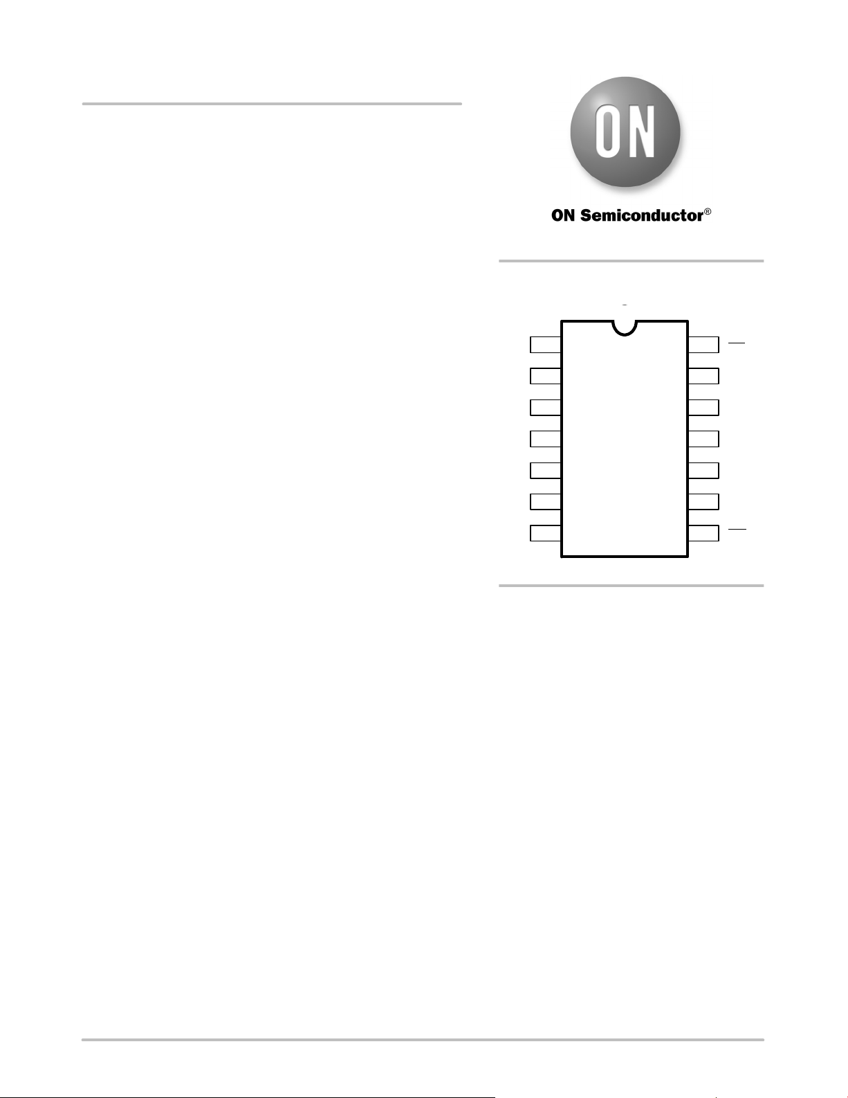
PIN ASSIGNMENT
TxD
GND
2
V
CC
3
RxD
4
V
IO
5
6
EN WAKE
INH
7
NCV7341
(Top View)
141
13
12
11
10
9
8
PC20060727.1
STB
CANH
CANL
V
SPLIT
VBAT
ERR
ORDERING INFORMATION
See detailed ordering and shipping information in the package
dimensions section on page 17 of this data sheet.
Typical Applications
• Automotive
• Industrial Networks
*For additional information on our Pb−Free strategy and soldering details, please
download the ON Semiconductor Soldering and Mounting Techniques
Reference Manual, SOLDERRM/D.
© Semiconductor Components Industries, LLC, 2009
May, 2009 − Rev. 4
1 Publication Order Number:
NCV7341/D
Page 2

NCV7341
Table 1. TECHNICAL CHARACTERISTICS
Symbol Parameter Condition Max Max Unit
V
CC
V
IO
V
EN
V
STB
V
TxD
V
RxD
V
ERR
V
CANH
V
CANL
V
SPLIT
V
O(dif)(bus_dom)
CM
range
C
load
t
pd(rec−dom)
t
pd(dom−rec)
T
J
ESD
HBM
Supply Voltage for the Core Circuitry 4.75 5.25 V
Supply Voltage for the Digital Interface 2.8 5.25 V
DC Voltage at Pin EN −0.3 VIO + 0.3 V
DC Voltage at Pin STB −0.3 VIO + 0.3 V
DC Voltage at Pin TxD −0.3 VIO + 0.3 V
DC Voltage at Pin RxD −0.3 VIO + 0.3 V
DC Voltage at Pin ERR −0.3 VIO + 0.3 V
DC Voltage at Pin CANH 0 < VCC < 5.25 V; No Time Limit −58 +58 V
DC Voltage at Pin CANL 0 < VCC < 5.25 V; No Time Limit −58 +58 V
DC Voltage at Pin V
SPLIT
Differential Bus Output Voltage in Dominant
0 < VCC < 5.25 V; No time Limit −58 +58 V
42.5 W < RLT < 60 W
1.5 3 V
State
Input Common−Mode Range for Comparator Guaranteed Differential Receiver
−35 +35 V
Threshold and Leakage Current
Load Capacitance on IC Outputs 15 pF
Propagation Delay TxD to RxD See Figure 6 90 230 ns
Propagation Delay TxD to RxD See Figure 6 90 245 ns
Junction Temperature −40 150 °C
ESD Level, Human Body Model Pins CANH, CANL, V
WAKE, V
other Pins
BAT
SPLIT
,
−4
−3
4
3
kV
http://onsemi.com
2
Page 3
BLOCK DIAGRAM
NCV7341
TxD
EN
STB
ERR
RxD
1
6
14
8
4
VIO
VIO
VIO
VIO
5
Level
shifter
7
Timer
Digital
Control
Block
VBATINH
10
POR
Thermal
shutdown
Driver
control
Wake −up
Filter
Clock
VCC
3
VCC
V
SPLIT
Rec
Low Power
Rec
VCC/2
”Active”
26 kW
12
13
11
CANH
VSPLIT
CANL
26 kW
WAKE
VIO
+
−
9
PC20060921.1
NCV7341
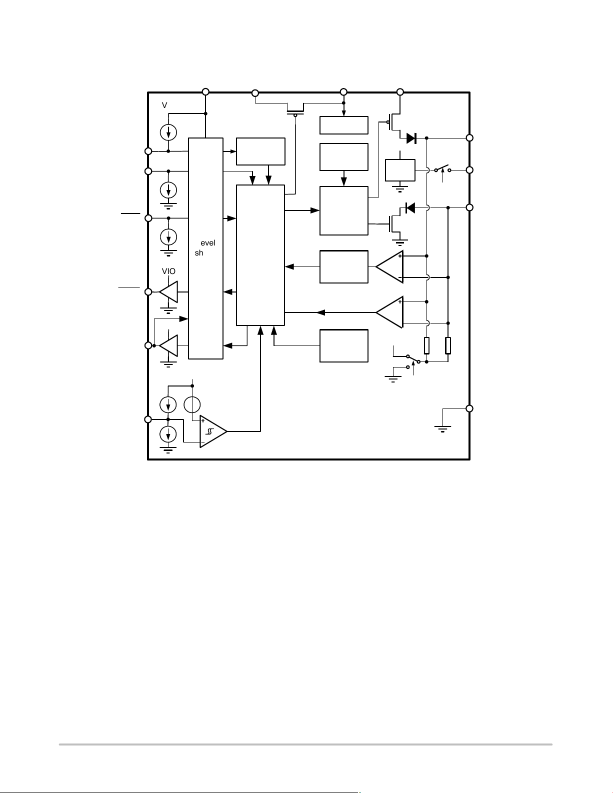
Figure 1. Block Diagram
”Active”
2
GND
http://onsemi.com
3
Page 4
TYPICAL APPLICATION SCHEMATICS
NCV7341
100nF
VCC
CAN
controller
x mF*
TxD
EN
STB
RxD
ERR
OUT
100 nF
5
3710
1
6
14
4
8
5V−Reg
VCC
NCV7341
2
VBATINHVio
13
11
12
9
IN
WAKE
2.7 kW
CANH
V
SPLIT
CANL
1kW
RLT=60W
GND GND
Note (*): Value depending on regulator
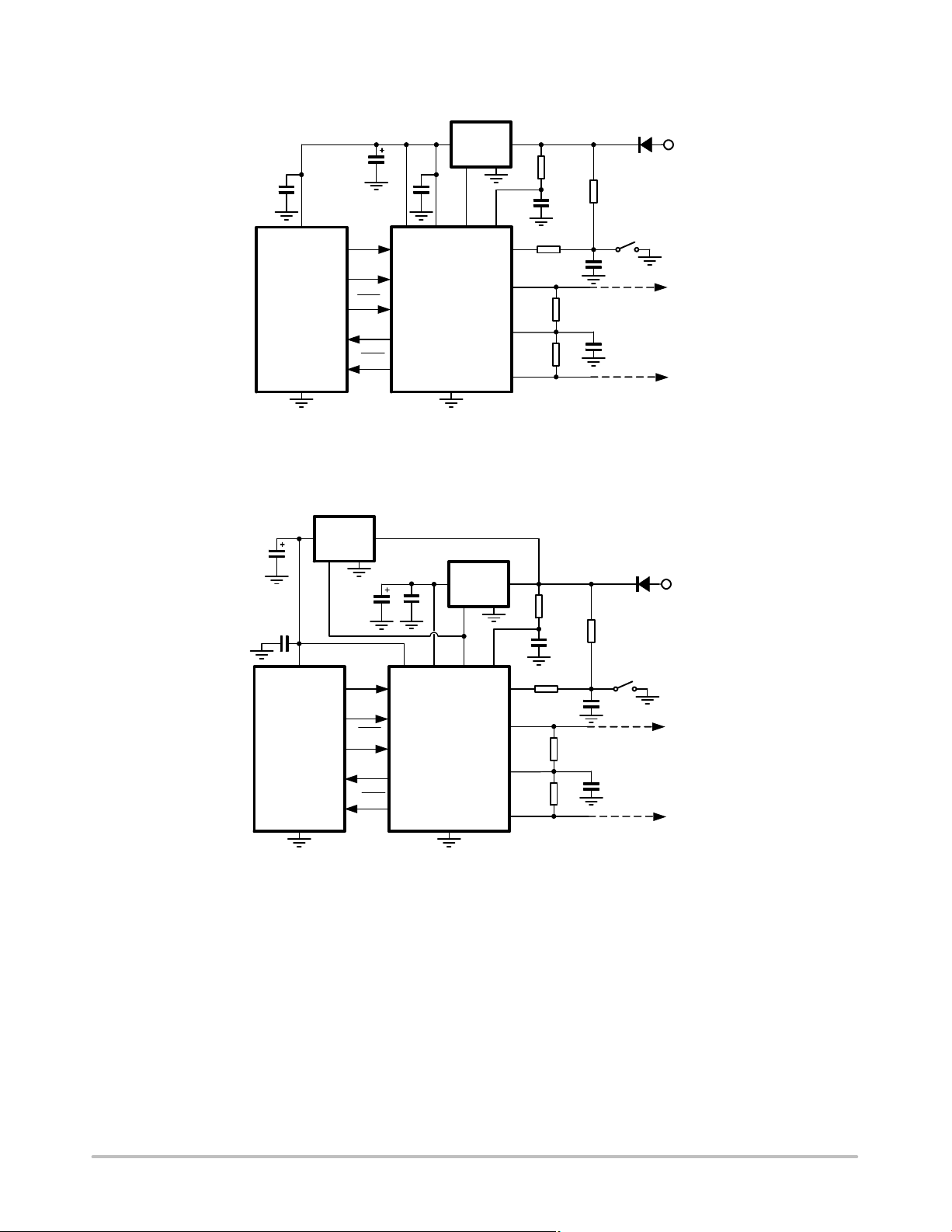
Figure 2. Application Diagram with a 5V CAN Controller
OUT IN
x mF*
100 nF
controller
3V−reg
x mF*
Vcc
CAN
GND GND
TxD
EN
STB
RxD
ERR
Vio
5
1
6
14
4
8
OUT
100 nF
Vcc
37
5V−reg
INH
NCV7341
2
VBAT
10
13
11
12
9
IN
WAKE
2.7 kW
CANH
V
SPLIT
CANL
1kW
10 nF
RLT=60W
10 nF
RLT=60W
PC20060921.4
R
=60W
LT
180 kW
10 nF
CLT= 4.7 nF
180 kW
10 nF
C
= 4.7 nF
LT
VBAT
CAN
BUS
VBAT
CAN
BUS
Note (*): Value depending on regulator
Figure 3. Application Diagram with a 3V CAN Controller
http://onsemi.com
4
PC20060921.4
Page 5
PIN DESCRIPTION
NCV7341
TxD
GND
2
V
CC
3
RxD
4
V
IO
5
6
EN WAKE
INH
7
NCV7341
141
13
12
11
10
9
8
PC20060727.1
STB
CANH
CANL
V
SPLIT
VBAT
ERR
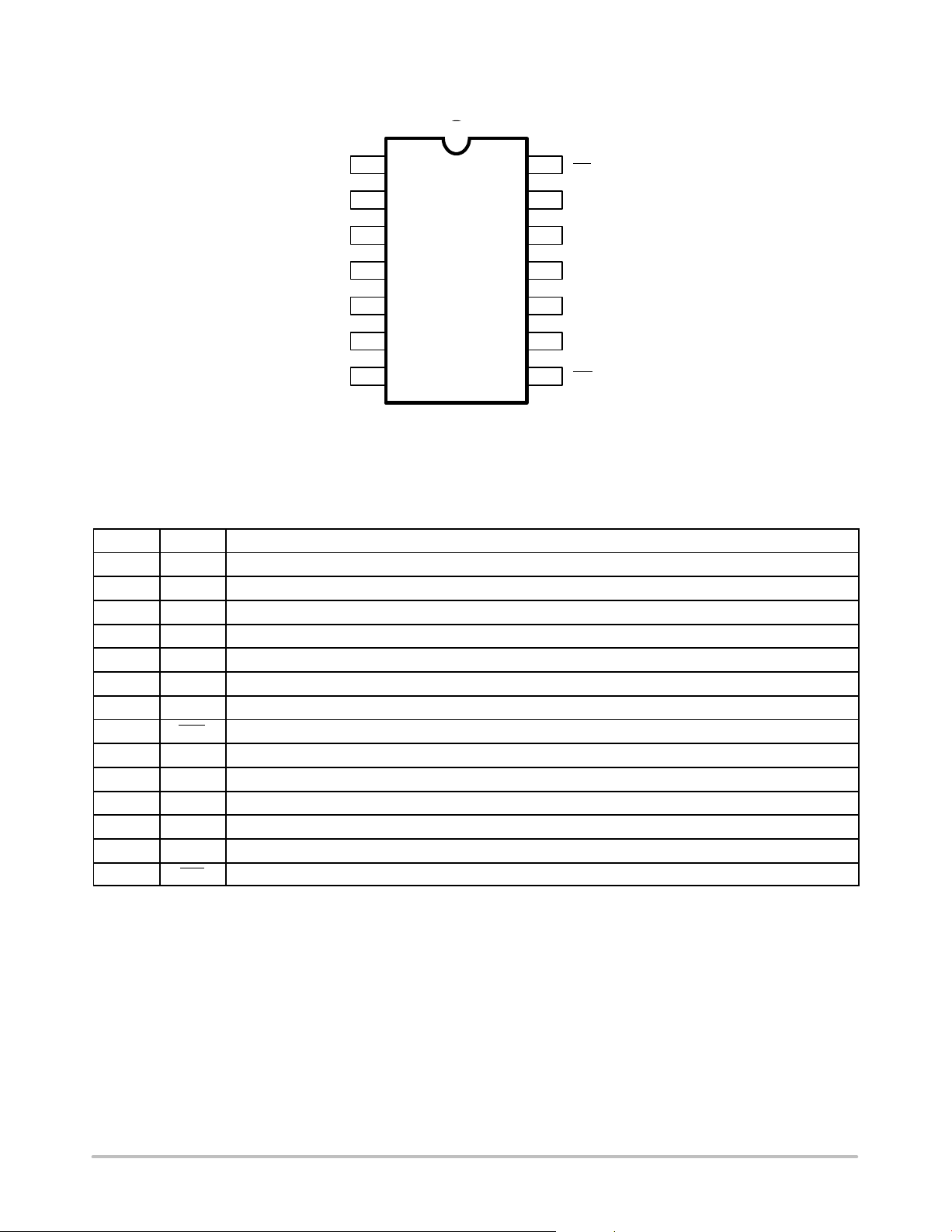
Figure 4. NCV7340 Pin Assignment
Table 2. PIN DESCRIPTION
Pin Name Description
1 TxD Transmit data input; low level = dominant on the bus; internal pull−up current
2 GND Ground
3 V
4 RxD Receive data output; dominant bus => low output
5 V
6 EN Enable input; internal pull−down current
7 INH High voltage output for controlling external voltage regulators
8
ERR Digital output indicating errors and power−up; active low
9 WAKE Local wake−up input
10 V
11 V
SPLIT
12 CANL Low−level CAN bus line (low in dominant)
13 CANH High−level CAN bus line (high in dominant)
14 STB Stand−by mode control input; internal pull−down current
Supply voltage for the core circuitry and the transceiver
CC
Supply voltage for the CAN controller interface
IO
Battery supply connection
BAT
Common−mode stabilization output
http://onsemi.com
5
Page 6
NCV7341
FUNCTIONAL DESCRIPTION
OPERATING MODES
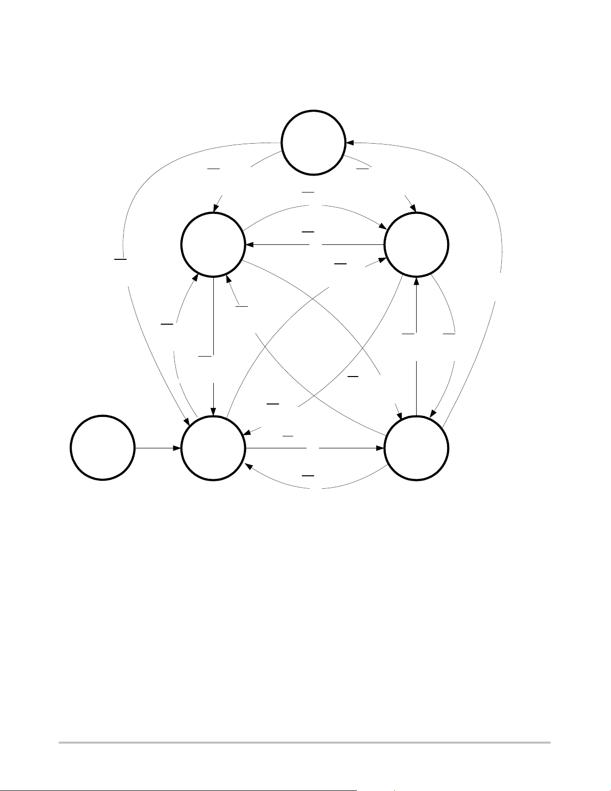
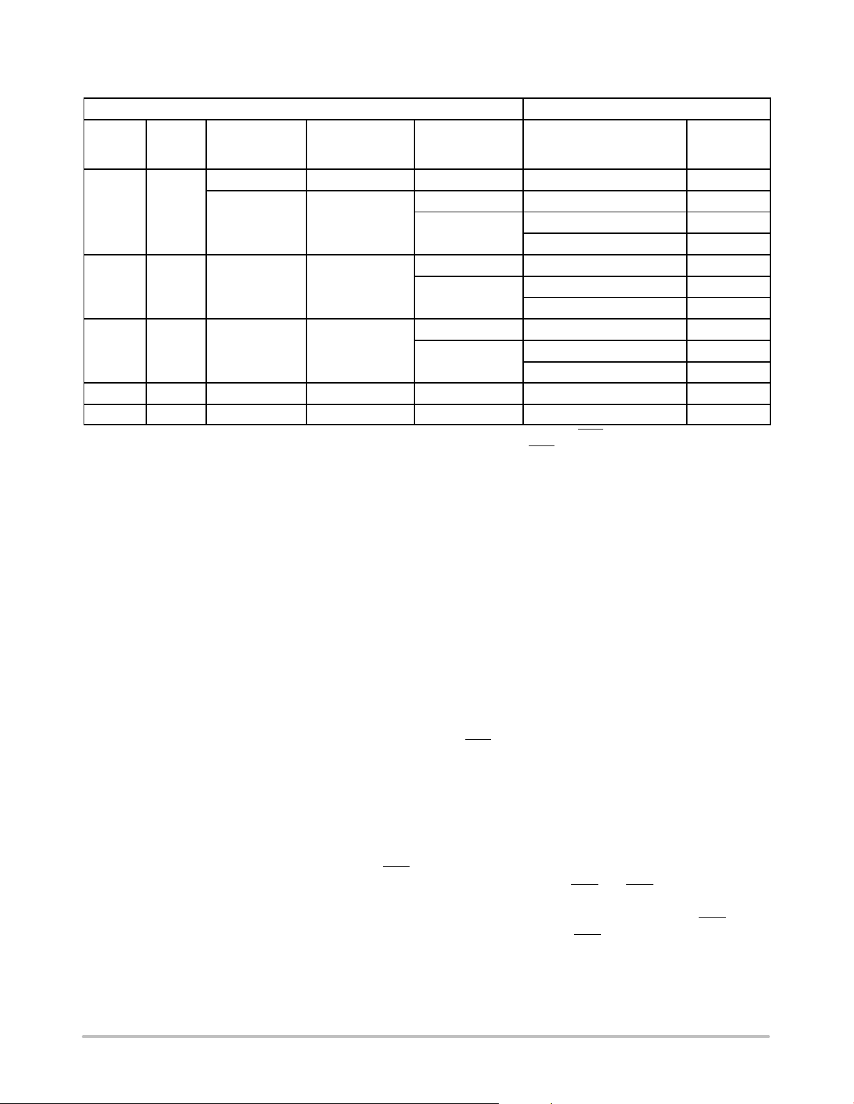
Operation modes of NCV7341 are shown in Figures 5 and in Table 3.
SLEEP
MODE
POWER
UP
STB = L
and
flags set
VCC/VIO undervoltage flag reset
RECEIVE
STB = H
and
EN = L
(EN = L or flags set)
STANDBY
STB = H and EN = L
and
ONLY
MODE
STB = H
and
EN = L
STB = L
and
MODE
STB = H
and
EN = H
STB = H
and
EN = L
STB = L
and
EN = L
STB = L and EN = H
and
flags reset
STB = H and EN = H
and
VCC/VIO undervoltage flag reset
NORMAL
MODE
STB = H
and
EN = H
STB = H
and
EN = H
STB = L and EN = H
and
flags reset
GOTO
SLEEP
MODE
STB = L
and
EN = H
flags reset
and
t > t
h(min)
STB = L
and
(EN = L or flags set)
LEGEND
”Flags set” : wake−up or power−up
”Flags reset” : not (wake−up or power−up)
Figure 5. Operation Modes
http://onsemi.com
6
PC20060921.2
Page 7
NCV7341
Table 3. OPERATION MODES
Conditions Transceiver Behavior
VCC/V
Undervoltage
Pin STB Pin EN
X X
Low Low Reset Reset
Low High Reset Reset
High Low Reset Reset X Receive−only High
High High Reset Reset X Normal High
Normal Mode
IO
Flag
Set X X Sleep Floating
Reset Set
In Normal mode, the transceiver is able to communicate
via the bus lines. The CAN controller can transmit data to the
bus via TxD pin and receive data from the bus via Pin RxD.
The bus lines (CANH and CANL) are internally biased to
V
/2 via the common−mode input resistance. Pin V
CC
is also providing voltage VCC/2 which can be further used
to externally stabilize the common mode voltage of the bus
– see Figure 2 and Figure 3. Pin INH is active (pulled high)
so that the external regulators controlled by INH Pin are
switched on.
Receive−Only Mode
In Receive−only mode, the CAN transmitter is disabled.
The CAN controller can still receive data from the bus via
RxD Pin as the receiver part remains active. Equally to
normal mode, the bus lines (CANH and CANL) are
internally biased to V
voltage V
Standby Mode
/2. Pin INH is also active (pulled high).
CC
/2 and Pin V
CC
Standby mode is a low−power mode. Both the transmitter
and the receiver are disabled and a very low−power
differential receiver monitors the CAN bus activity. Bus
lines are biased internally to ground via the common mode
input resistance and Pin V
is high−impedant (floating).
SPLIT
A wake−up event can be detected either on the CAN bus or
on the WAKE Pin. A valid wake−up is signaled on pins ERR
and RxD. Pin INH remains active (pulled high) so that the
external regulators controlled by INH Pin are switched on.
Go−To−Sleep Mode
Go−To −Sleep mode is an intermediate state used to put the
transceiver into sleep mode in a controlled way.
Go−To −Sleep mode is entered when the CAN controller
VBAT
Undervoltage
Flag
is providing
SPLIT
SPLIT
Power−up or
Wakeup Flag
Set Standby High
Reset
Set Stand−by High
Reset
Set Stand−by High
Reset
puts pin EN to High and STB
of Pins EN and STB
of t
and neither a wake−up nor a power−up event occur
h(min)
Operating Mode Pin INH
If in sleep, then no change Floating
otherwise stand−by High
If in sleep, then no change Floating
otherwise stand−by High
If in sleep, then no change Floating
otherwise go−to−sleep High
Pin to Low. If the logical state
is kept unchanged for minimum period
during this time, the transceiver enters sleep mode. While in
go−to−sleep mode, the transceiver behaves identically to
stand−by mode.
Sleep Mode
Sleep mode is a low−power mode in which the
consumption is further reduced compared to stand−by
mode. Sleep mode can be entered via go−to−sleep mode or
in case an undervoltage on either V
or VIO occurs for
CC
longer than the under−voltage detection time. The
transceiver behaves identically to standby mode, but the
INH Pin is deactivated (left floating) and the external
regulators controlled by INH Pin are switched off. In this
way, the V
consumption is reduced to a minimum. The
BAT
device will leave sleep mode either by a wake−up event (in
case of a CAN bus wake−up or via Pin WAKE) or by putting
Pin STB
high (as long as an under−voltage on VCC or V
is not detected).
Internal Flags
The transceiver keeps several internal flags reflecting
conditions and events encountered during its operation.
Some flags influence the operation mode of the transceiver
(see Figure 5 and Table 3). Beside the undervoltage and the
TxD dominant timeout flags, all others can be read by the
CAN controller on Pin ERR
. Pin ERR signals internal flags
depending on the operation mode of the transceiver. An
overview of the flags and their visibility on Pin ERR
in Table 4. Because the ERR
Pin uses negative logic, it will
be pulled low if the signaled flag is set and will be pulled
high if the signaled flag is reset.
IO
is given
http://onsemi.com
7
Page 8
NCV7341
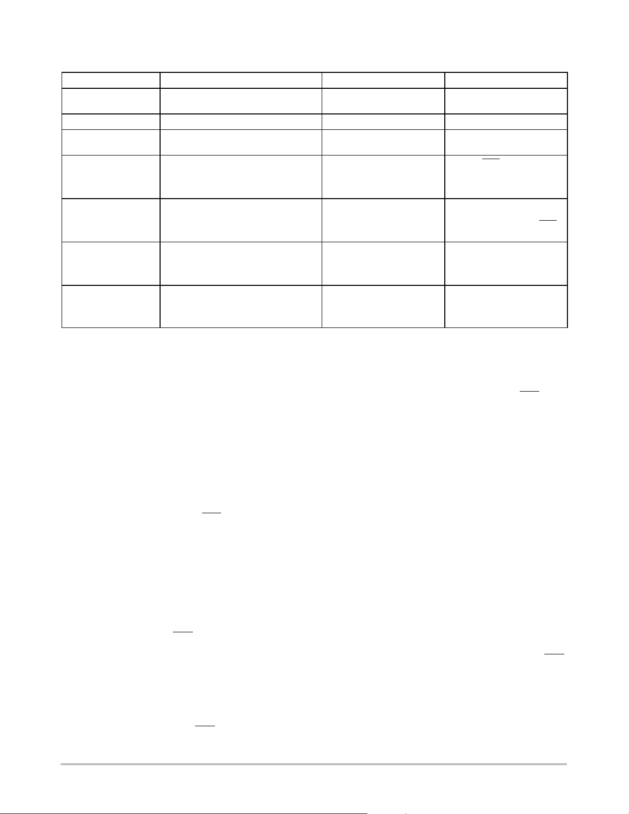
Table 4. INTERNAL FLAGS AND THEIR VISIBILITY
Internal Flag Set Condition Reset Condition Visibility on Pin ERR
VCC/V
V
Powerup V
Wake−up When remote or local wake−up is
Local Wake−up When local wake−up is detected
Failure Pin TxD clamped low or
Bus Failure
(NCV7341D20)
Undervoltage VCC < V
IO
Undervoltage V
BAT
IO(SLEEP)
longer than t
longer than t
(PWUP)
UV(VCC)
UV(VIO)
CC(SLEEP)
or VIO < V
< V
BAT
BAT(STB)
rises above VBAT
BAT
(V
connection to the transceiver)
BAT
detected
(i.e.via pin WAKE)
overtemperature
One of the bus lines shorted to ground
or supply during four consecutive
transmitted dominants
At wake−up or power−up No
When V
When normal mode is
entered
At power−up or when normal
mode is entered or when
VCC/VIO undervoltage flag is
set
At power−up or when leaving
normal mode
When entering normal mode
or when RxD is Low while
TxD is high (provided all
failures disappeared)
No bus line short (to ground
or supply) detected during
four consecutive dominant bit
transmissions
recovers No
BAT
In receive−only mode. Not
going from normal mode
Both on ERR and RxD (both
pulled to low). In
go−to−sleep, standby and
sleep mode.
In normal mode before 4
consecutive dominant
symbols are sent. Then ERR
pin becomes High again
Overtemperature condition
observable in receive−only
mode entered from normal
mode
In normal mode
VCC/VIO Undervoltage Flag
The VCC/VIO undervoltage flag is set if VCC supply drops
below V
CC(sleep)
supply drops below V
level for longer than t
level for longer than t
IO(sleep)
UV(VCC)
or V
UV(VIO)
IO
If the flag is set, the transceiver enters sleep mode. After a
waiting time identical to the undervoltage detection times
t
UV(VCC)
and t
UV(VIO)
, respectively, the flag can be reset
either by a valid wake−up request or when the powerup flag
is set. During this waiting time, the wakeup detection is
blocked.
VBAT Under−voltage Flag
The flag is set when V
supply drops below V
BAT
BAT(STB)
level. The transceiver will enter the standby mode. The flag
is reset when V
enters the mode defined by inputs STB
Power−up Flag
This flag is set when V
below V
BAT(PWUP)
connection of the transceiver to the battery. The V
supply recovers. The transceiver then
BAT
and EN.
supply recovers after being
BAT
level, which corresponds to a
CC/VIO
undervoltage flag is cleared so that the transceiver cannot
enter the Go−to−sleep Mode, ensuring that INH Pin is high
and the external voltage regulators are activated at the
battery connection. In Receive−only mode, the powerup
flag can be observed on the ERR
Pin. The flag is reset when
Normal mode is entered.
Wake−up Flag
This flag is set when the transceiver detects a valid
wake−up request via the bus or via the WAKE Pin. Setting
the wake−up flag is blocked during the waiting time of the
V
immediately propagated to Pins ERR
that supplies V
undervoltage flag. The wake−up flag is
CC/VIO
and RxD – provided
and VIO are available. The wake−up flag
CC
is reset at power−up or when V
undervoltage occurs
CC/VIO
or when Normal mode is entered.
Local wake−up Flag
.
This flag is set when a valid wake−up request through
WAKE Pin occurs. It can be observed on the ERR
normal mode. It can only be set when the powerup flag is
reset. The local wake−up flag is reset at powerup or at
leaving Normal mode.
Failure Flag
The failure flag is set in one of the following situations:
• TxD Pin is Low (i.e. dominant is requested by the CAN
controller) for longer than t
dom(TxD
condition, the transmitter is disabled so that a bus
lockup is avoided in case of an application failure
which would drive permanent dominant on the bus. The
transmitter remains disabled until the failure flag is
reset.
) − Under this
• Overtemperature − If the junction temperature reaches
, the transmitter is disabled in order to protect it
T
J(SD)
from overheating and the failure flag is set. The
transmitter remains disabled until the failure flag is
reset.
The failure flag is reset when Normal mode is entered or
when TxD pin is High while RxD pin is Low. In case of
overtemperature, the failure flag is observable on pin ERR
Bus Failure Flag (NCV7341D20)
The transmitter of the NCV7341D20 device version
allows bus failure detection. During dominant bit
transmission, a short of the CANH or CANL line to ground
or supply (V
short circuit condition lasts for four consecutive dominant
, VBAT or other) is internally detected. If the
CC
Pin in
.
http://onsemi.com
8
Page 9

NCV7341
transmissions, an internal bus failure flag is set and made
immediately visible through a Low level on the ERR
pin.
The transmission and reception circuitry continues to
function.
When four consecutive dominant transmissions succeed
without a bus line short being detected, the internal bus
failure flag is reset and ERR
Split Circuit
The V
Pin is operational only in normal and
SPLIT
pin is released to High level.
receive−only modes. It is floating in standby and sleep
modes. The V
can be connected as shown in Figure 2
SPLIT
and Figure 3 and its purpose is to provide a stabilized DC
voltage of V
/2 to the bus avoiding possible steps in the
CC
common−mode signal, therefore reducing EME. These
unwanted steps could be caused by an unpowered node on
the network with excessive leakage current from the bus that
shifts the recessive voltage from its nominal V
Wake−up
/2 level.
CC
The transceiver can detect wake−up events in stand−by,
go−to−sleep and sleep modes. Two types of wake−up events
are handled – remote wake−up via the CAN bus or a local
wake−up via the WAKE pin. A valid remote wake−up is
recognized after two dominant states of the CAN bus of at
least t
least t
, each of them followed by a recessive state of at
dom
.
rec
A local wake−up is detected after a change of state (High
to Low, or Low to High) on WAKE Pin which is stable for
at least t
. To increase the EMS level of the WAKE Pin,
WAKE
an internal current source is connected to it. If the state of the
WAKE Pin is stable at least for t
, the direction of the
WAKE
current source follows (pulldown current for Low state,
pullup current for High state). It is recommended to connect
Pin WAKE either to GND or VBAT if it’s not used in the
application.
Fail Safe Features
Fail safe behavior is ensured by the detection functions
associated with the internal flags.
Furthermore, a current−limiting circuit protects the
transmitter output stage from damage caused by accidental
short circuit to either positive or negative supply voltage,
although power dissipation increases during this fault
condition.
The Pins CANH and CANL are protected from
automotive electrical transients (according to ISO 7637; see
Figure 9). Pins TxD is pulled high and Pins STB
and EN are
pulled low internally should the input become disconnected.
Pins TxD, STB
reverse supply should the V
, EN and RxD will be floating, preventing
supply be removed.
IO
http://onsemi.com
9
Page 10
NCV7341
ELECTRICAL CHARACTERISTICS
Definitions
All voltages are referenced to GND (Pin 2). Positive
currents flow into the IC. Sinking current means the current
is flowing into the pin; sourcing current means the current
is flowing out of the pin.
Absolute Maximum Ratings
Stresses above those listed in the following table may
cause permanent device failure. Exposure to absolute
maximum ratings for extended periods may affect device
reliability.
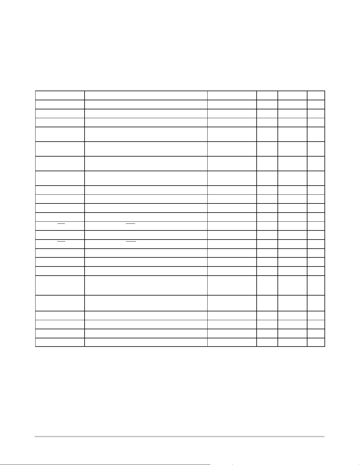
Table 5. ABSOLUTE MAXIMUM RATINGS
Symbol Parameter Conditions Min. Max. Unit
V
BAT
V
CC
V
IO
V
CANH
V
CANL
V
CANL−VCANH
V
SPLIT
V
INH
V
WAKE
V
TxD
V
RxD
V
STB
V
EN
V
ERR
V
tran(CANH)
V
tran(CANL)
V
tran(VSPLIT)
V
esd(CANL/CANH/
VSPLIT, VBAT, WAKE)
V
esd
Latch−up Static latch−up at all pins (Note 3) 120 mA
T
stg
T
amb
T
junc
Stresses exceeding Maximum Ratings may damage the device. Maximum Ratings are stress ratings only. Functional operation above the
Recommended Operating Conditions is not implied. Extended exposure to stresses above the Recommended Operating Conditions may affect
device reliability.
1. Applied transient waveforms in accordance with ISO 7637 part 3, test pulses 1, 2, 3a, and 3b (see Figure 9).
2. Standardized human body model electrostatic discharge (ESD) pulses in accordance to MIL883 method 3015.7.
3. Static latch-up immunity: Static latch-up protection level when tested according to EIA/JESD78.
4. Standardized charged device model ESD pulses when tested according to EOS/ESD DS5.3-1993.
Supply voltage −0.3 58 V
Supply voltage −0.3 +7 V
Supply voltage −0.3 +7 V
DC voltage at pin CANH 0 < VCC < 5.25 V;
−58 +58 V
no time limit
DC voltage at pin CANL 0 < VCC < 5.25 V;
−58 +58 V
no time limit
DC voltage between bus pins CANH and CANL 0 < VCC < 5.25 V;
−58 +58 V
no time limit
DC voltage at pin VSPLIT 0 < VCC < 5.25 V;
−58 +58 V
no time limit
DC voltage at pin INH −0.3 VBAT+0.3 V
DC voltage at pin WAKE −0.3 58 V
DC voltage at pin TxD −0.3 7 V
DC voltage at pin RxD −0.3 VIO + 0.3 V
DC voltage at pin STB −0.3 7 V
DC voltage at pin EN −0.3 7 V
DC voltage at pin ERR −0.3 VIO + 0.3 V
Transient voltage at pin CANH (Note 1) −300 +300 V
Transient voltage at pin CANL (Note 1) −300 +300 V
Transient voltage at pin VSPLIT (Note 1) −300 +300 V
Electrostatic discharge voltage at pins intended to be
wired outside of the module
(CANH, CANL, V
, VBAT, WAKE)
SPLIT
Electrostatic discharge voltage at all other pins (Note 2)
(Note 2)
(Note 4)
(Note 4)
−4
−500
−3
−500
4
500
3
500
kV
kV
Storage temperature −50 +150 °C
Ambient temperature −50 +125 °C
Maximum junction temperature −50 +180 °C
V
V
http://onsemi.com
10
Page 11
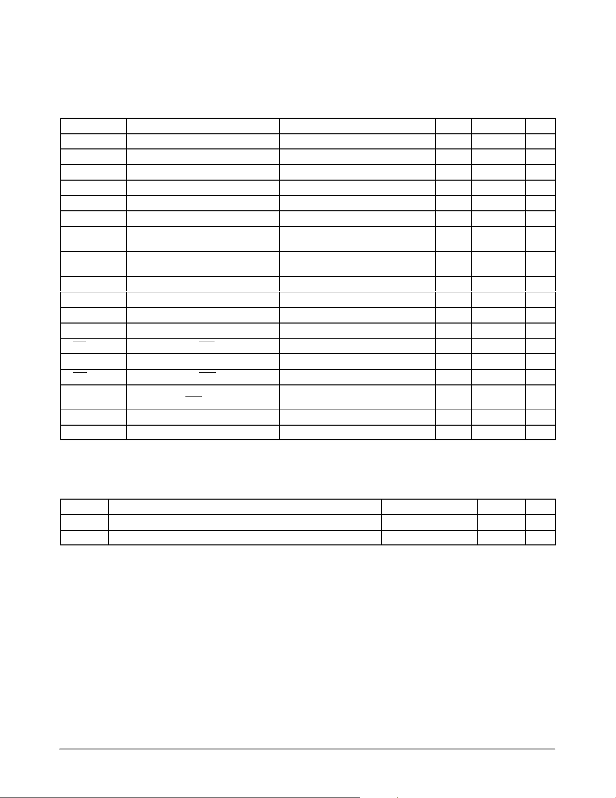
NCV7341
Operating Conditions
Operating conditions define the limits for functional operation, parametric characteristics and reliability specification of the
device. Functionality of the device is not guaranteed outside the operating conditions.
Table 6. OPERATING RANGES
Symbol Parameter Conditions Min Max Unit
V
BAT
V
BAT_SLEEP
V
CC
V
IO
V
CANH
V
CANL
V
CANL−VCANH
V
SPLIT
V
INH
V
WAKE
V
TxD
V
RxD
V
STB
V
EN
V
ERR
C
LOAD
T
A
T
J
1. In the sleep mode, all relevant parameters are guaranteed only for V
and the functionality is also guaranteed, but some parameters might get slightly out of the specification − e.g. the wakeup detection
thresholds.
Supply Voltage 5.0 50 V
Supply Voltage in the Sleep Mode (Note 1) 6.0 50 V
Supply Voltage 4.75 5.25 V
Supply Voltage 2.8 5.25 V
DC Voltage at Pin CANH Receiver Function Guaranteed −35 +35 V
DC Voltage at Pin CANL Receiver Function Guaranteed −35 +35 V
DC Voltage Between Bus Pins CANH
Receiver Function Guaranteed −35 +35 V
and CANL
DC Voltage at Pin V
SPLIT
DC Voltage at Pin INH −0.3 V
DC Voltage at Pin WAKE −0.3 V
Leakage and Current Limitation are
Guaranteed
−35 +35 V
+ 0.3 V
BAT
+ 0.3 V
BAT
DC Voltage at Pin TxD −0.3 VIO + 0.3 V
DC Voltage at Pin RxD −0.3 VIO + 0.3 V
DC Voltage at Pin STB −0.3 VIO + 0.3 V
DC Voltage at Pin EN −0.3 VIO + 0.3 V
DC Voltage at Pin ERR −0.3 VIO + 0.3 V
Capacitive Load on Digital Outputs
(Pins RxD and ERR
)
15 pF
Ambient Temperature −40 +125 °C
Maximum Junction Temperature −40 +150 °C
> 6 V. For V
BAT
between 5 V and 6 V, no power−on−reset will occur
BAT
Table 7. THERMAL CHARACTERISTICS
Symbol Parameter Conditions Value Unit
R
th(vj−a)
R
th(vj−a)
Thermal Resistance from Junction−to−Ambient in SOIC−14 Package 1S0P PCB 128 K/W
Thermal Resistance from Junction−to−Ambient in SOIC−14 Package 2S2P PCB 70 K/W
http://onsemi.com
11
Page 12
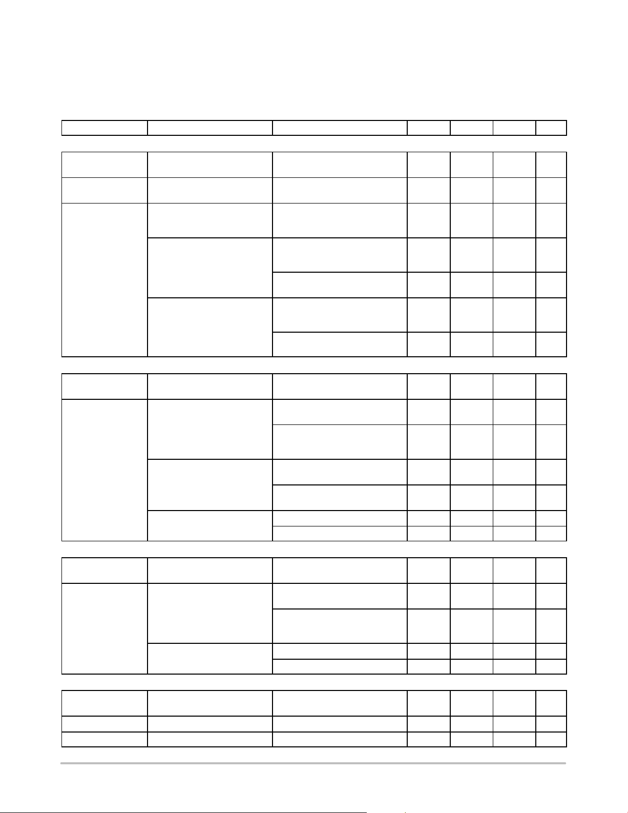
NCV7341
Characteristics
The characteristics of the device are valid for operating conditions defined in Table 7 and the bus lines are considered to be
loaded with R
Table 8. DC CHARACTERISTICS
Symbol Parameter Conditions Min Typ Max Unit
SUPPLY (PIN VBAT)
VBAT
(STB)
VBAT
(PWUP)
I
VBAT
SUPPLY (PIN VCC)
V
CC(SLEEP)
I
VCC
SUPPLY (PIN VIO)
V
IO(SLEEP)
I
VIO
TRANSMITTER DATA INPUT (PIN TxD)
V
IH
V
IL
I
IH
= 60 W, unless specified otherwise.
LT
Level for Setting V
Undervoltage Flag
BAT
Level for Setting Powerup
Flag
V
Current Consumption in
BAT
Normal and Receive−Only
Modes
V
Current Consumption in
BAT
Standby and Go−to−Sleep
Modes. The total supply
current is drawn partially from
V
and partially from VCC.
BAT
V
Current Consumption in
BAT
Sleep Mode. The supply
current is drawn from V
.
only
BAT
VCC Level for Setting VCC/V
Undervoltage Flag
VCC Current Consumption in
Normal or Receive−Only
Mode
VCC Current Consumption in
Standby and Go−to−Sleep
Mode. The total supply
current is drawn partially from
V
and partially from VCC.
BAT
VCC Current Consumption in
Sleep Mode
VIO Level for Setting VCC/V
Undervoltage Flag
VIO Current Consumption in
Normal or Receive−Only
Mode
VIO Current Consumption in
Standby or Sleep Mode
High−Level Input Voltage Output Recessive 0.7V
Low−Level Input Voltage Output Dominant −0.3 − 0.3V
High−Level Input Current V
VCC = 5 V 2.75 3.3 4.5 V
VCC = 0 V 2.75 3.3 4.5 V
INH and WAKE Not Loaded 1.0 10 40
V
> 4.75 V, V
VCC
V
= V
INH
T
V
V
V
V
T
V
V
V
IO
WAKE
< 100°C
amb
> 4.75 V, V
VCC
= V
INH
WAKE
= V
VCC
INH
= V
WAKE
amb
VCC
WAKE
BAT
VBAT
< 100°C
= V
INH
= V
VBAT
= 12 V 2.75 3.3 4.5 V
Normal Mode:
V
= 0 V, i.e. Dominant
TxD
Normal Mode: V
Recessive (or Receive−Only
= V
= V
= V
= V
> 2.8 V
VIO
VBAT
> 2.8 V
VIO
VBAT
= 0 V
VIO
= 12 V
= 0 V
VIO
= 12 V
= VIO, i.e.
TxD
= 12 V
8.0 12 22.5
= 12 V
10 20 50
25 55 80 mA
2.0 6.0 10 mA
Mode)
T
< 100°C 17.5
amb
6.5 12 19.5
T
< 100°C 1.0
amb
0.2 0.5 2.0
IO
Normal Mode:
V
= 0V, i.e. Dominant
TxD
Normal Mode: V
Recessive (or Receive−Only
= VIO, i.e.
TxD
0.9 1.6 2.0 V
100 350 1000
0 0.2 1.0
mode)
T
< 100°C 1.0
amb
0 0 5.0
− VIO +
TxD
= V
VIO
VIO
−5.0 0 +5.0
18
35
0.3
VIO
mA
mA
mA
mA
mA
mA
mA
mA
mA
mA
mA
mA
mA
V
V
mA
http://onsemi.com
12
Page 13
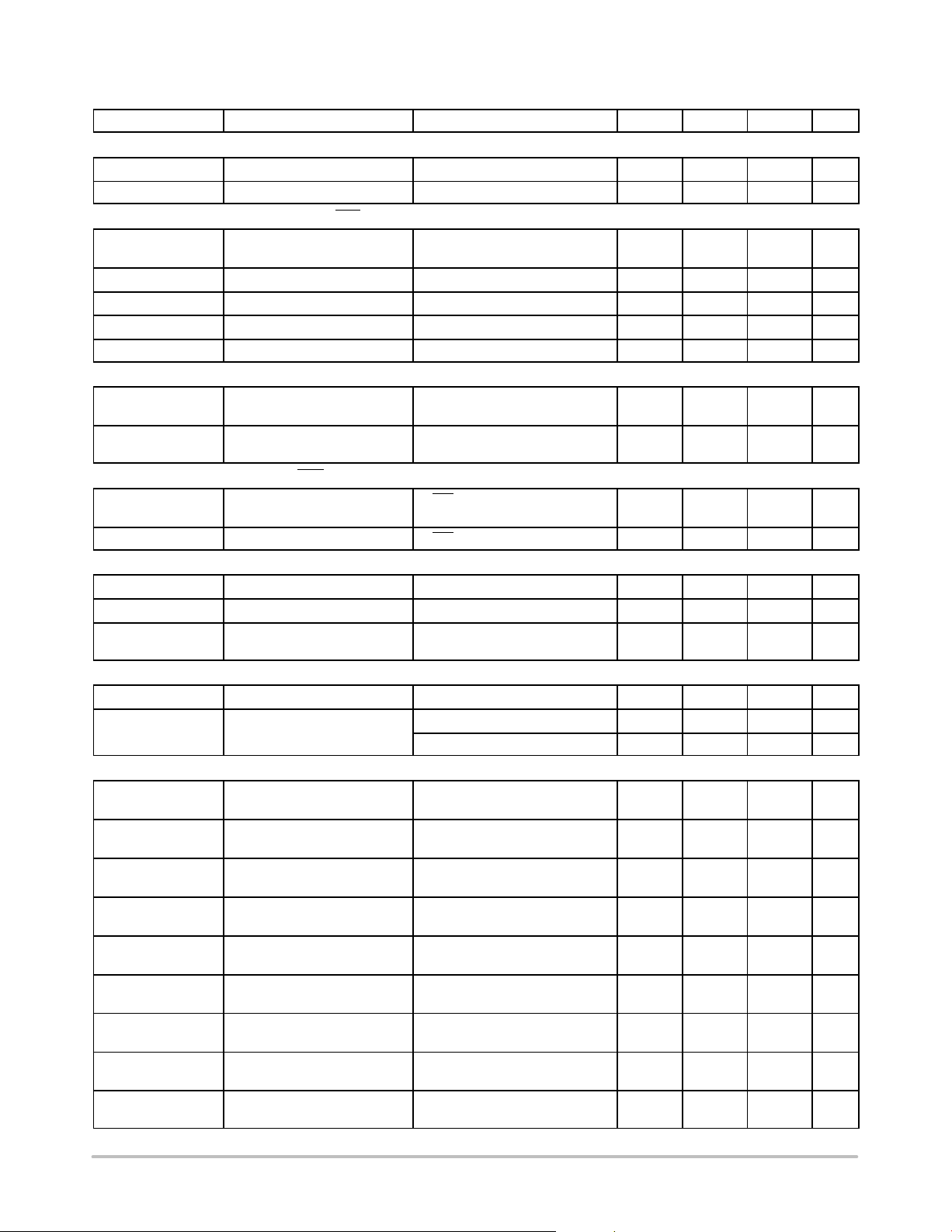
Table 8. DC CHARACTERISTICS
Symbol UnitMaxTypMinConditionsParameter
TRANSMITTER DATA INPUT (PIN TxD)
I
IL
C
i
STANDBY AND ENABLE INPUTS (PINS STB AND EN)
V
IH
V
IL
I
IH
I
IL
C
i
RECEIVER DATA OUTPUT (PIN RxD)
I
OH
I
OL
FLAG INDICATION OUTPUT (PIN ERR)
I
OH
I
OL
LOCAL WAKE−UP INPUT (PIN WAKE)
I
IH
I
IL
V
threshold
INHIBIT OUTPUT (PIN INH)
VH
DROP
I
LEAK
BUS LINES (PINS CANH AND CANL)
V
o(reces) (norm)
V
o(reces) (stby)
I
o(reces) (CANH)
I
o(reces) (CANL)
V
o(dom) (CANH)
V
o(dom) (CANL)
V
o(dif) (bus_dom)
V
o(dif) (bus_rec)
I
o(sc) (CANH)
Low−Level Input Current V
Input Capacitance Not Tested 1.0 5.0 10 pF
High−Level Input Voltage 0.7V
Low−Level Input Voltage −0.3 − 0.3V
High−Level Input Current V
Low−Level Input Current V
Input Capacitance 1.0 5.0 10 pF
High−Level Output Current V
Low−Level Output Current V
High−Level Output Current V
Low−Level Output Current V
High−Level Input Current V
Low−Level Input Current V
Threshold of the Local
Wake−up Comparator
High Level Voltage Drop
Leakage Current in Sleep
Mode
Recessive Bus Voltage V
Recessive Bus Voltage V
Recessive Output Current at
Pin CANH
Recessive Output Current at
Pin CANL
Dominant output Voltage at
Pin CANH
Dominant Output Voltage at
Pin CANL
Differential Bus Output
Voltage (V
CANH
− V
CANL
)
Differential Bus Output
Voltage (V
CANH
− V
CANL
)
Short−Circuit Output Current
at Pin CANH
NCV7341
= 0.3 V
TxD
STB
STB
RxD
V
VIO
RxD
V
TxD
ERR
V
VIO
ERR
WAKE
WAKE
VIO
= VEN = 0.7V
VIO
= VEN = 0 V −0.5 0 5.0
= V
− 0.4 V
VIO
= V
VCC
= 0.4 V
= 0 V Bus is Dominant
= V
− 0.4 V
VIO
= V
VCC
= 0.4 V 100 200 350
= V
− 1.9 V −1.0 −5.0 −10
VBAT
= V
− 3.1 V 1.0 5.0 10
VBAT
Sleep or Standby Mode V
I
= −180 mA
INH
T
< 100°C 0 − 1.0
amb
= V
TxD
Mode
TxD
Mode
−35 V < V
0 V < V
−35 V < V
0 V < V
V
TxD
V
TxD
V
TxD
42.5 W < RLT < 60 W
V
TxD
Load
V
CANH
; No Load, Normal
VCC
= V
; No Load, Standby
VCC
< +35 V;
CANH
< 5.25 V
CC
< +35 V;
CANL
< 5.25 V
VCC
= 0 V 3.0 3.6 4.25 V
= 0 V 0. 5 1.4 1.75 V
= 0 V; Dominant;
= VCC; Recessive; No
= 0 V; V
= 0 V −45 −70 −120 mA
TxD
−70 −250 −500
VIO
− VIO +
0.3
1.0 5.0 10
−1.0 −3.0 −6.0 mA
2.0 5.0 12 mA
−4.0 −20 −50
−
V
−
VBAT
3 V
VBAT
2.5 V
V
VBAT
2 V
50 200 800 mV
0 − 5.0
2.0 2.5 3.0 V
−100 0 100 mV
−2.5 − +2.5 mA
−2.5 − +2.5 mA
1.5 2.25 3.0 V
−120 0 +50 mV
VIO
mA
V
V
mA
mA
mA
mA
mA
mA
−
V
mA
mA
http://onsemi.com
13
Page 14
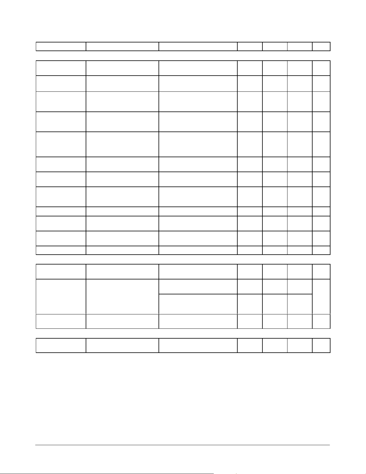
Table 8. DC CHARACTERISTICS
Symbol UnitMaxTypMinConditionsParameter
BUS LINES (PINS CANH AND CANL)
I
o(sc) (CANL)
V
i(dif) (th)
V
ihcm(dif) (th)
V
i(dif) (hys)
V
I(dif)_WAKE
R
i(cm) (CANH)
R
i(cm) (CANL)
R
i(cm)(m)
R
i(dif)
C
i(CANH)
C
i(CANL)
C
i(dif)
COMMON−MODE STABILIZATION (PIN V
V
SPLIT
I
SPLIT(i)
I
SPLIT(lim)
THERMAL SHUTDOWN
T
J(SD)
Short−Circuit Output Current
at Pin CANL
Differential Receiver Threshold
Voltage (see Figure 7)
Differential Receiver Threshold
Voltage for High
Common−Mode (see Figure 7)
Differential Receiver Input
Voltage Hysteresis
(see Figure 7)
Differential Receiver Input
Voltage for Bus Wake−up
Detection (in Sleep or
Standby Mode)
Common−Mode Input
Resistance at Pin CANH
Common−Mode Input
Resistance at Pin CANL
Matching between Pin CANH
and Pin CANL Common
Mode Input Resistance
Differential Input Resistance 25 50 75
Input Capacitance at Pin
CANH
Input Capacitance at Pin
CANL
Differential Input Capacitance V
Reference Output Voltage at
Pin V
SPLIT
V
Leakage Current
SPLIT
V
Limitation Current
SPLIT
(Absolute Value)
Shutdown Junction
Temperature
SPLIT
NCV7341
V
= 42 V; V
CANL
−12 V < V
−12 V < V
−35 V < V
−35 V < V
−35 V < V
−35V <V
−12 V < V
−12 V < V
V
V
V
CANH
TxD
TxD
TxD
= V
= V
= V
= V
CANL
CANH
CANL
CANH
CANL
CANH
CANH
CANH
CANL
CC
CC
CC
)
Normal mode;
−500 mA < I
Standby Mode
−27 V < V
SPLIT
Standby Mode
−27 V < V
T
amb
SPLIT
< 100°C
Normal Mode 1.3 3.0 5.0 mA
= 0 V 45 70 120 mA
TxD
< +12 V
0.5 0.7 0.9 V
< +12 V
< +35 V
0.35 0.7 1.00 V
< +35 V
< +35 V
50 70 100 mV
< +35 V
< +12 V
0.4 0.8 1.15 V
< +12 V
15 26 39
15 26 39
−3.0 0 +3.0 %
7.5 20 pF
7.5 20 pF
3.75 10 pF
SPLIT
< 500 mA
0.3 x
V
CC
0.5 x
V
CC
−50 +50 mA
< 40 V
−5.0 +5.0
< 40 V
150 160 180 °C
0.7 x
V
CC
kW
kW
kW
http://onsemi.com
14
Page 15
NCV7341
Table 9. AC CHARACTERISTICS
Symbol Parameter Conditions Min Typ Max Unit
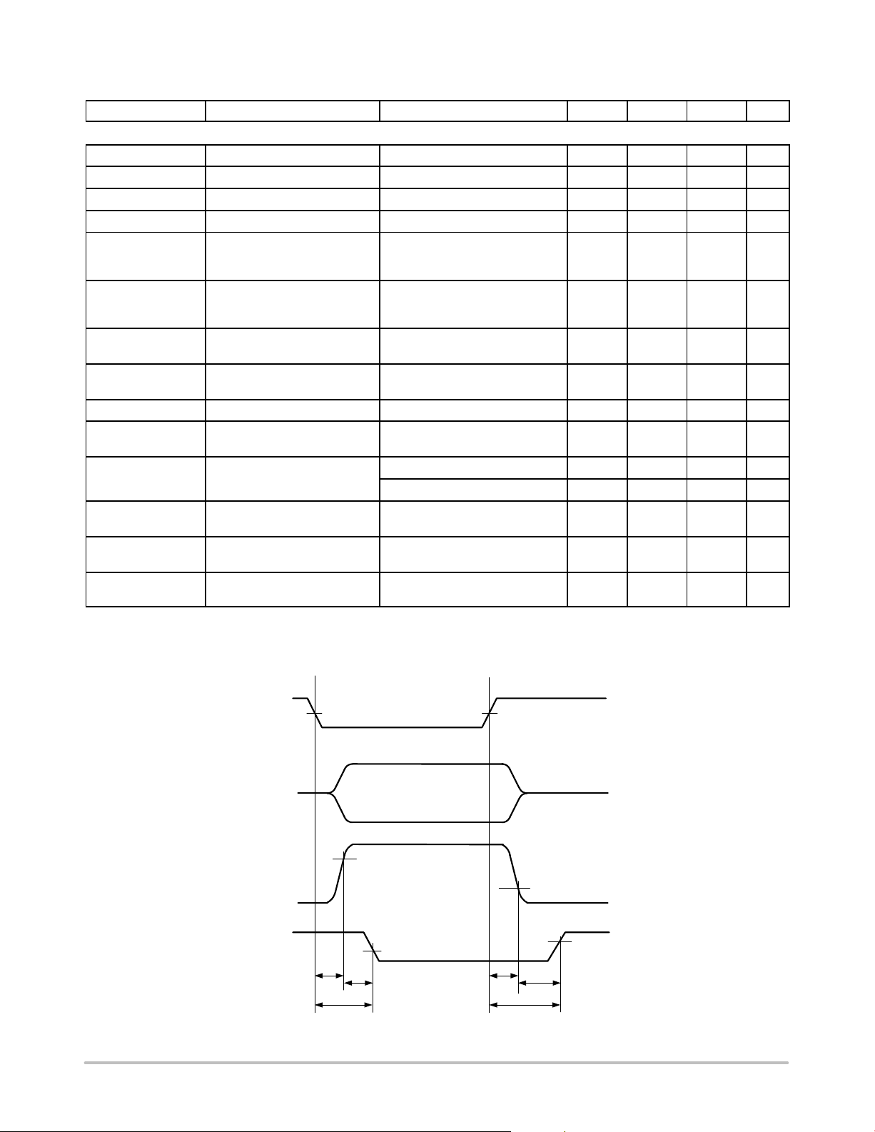
TIMING CHARACTERISTICS (Figure 6)
t
d(TxD−BUSon)
t
d(TxD−BUSoff)
t
d(BUSon−RxD)
t
d(BUSoff−RxD)
t
pd(rec−dom)
t
d(dom−rec)
t
UV(VCC)
t
UV(VIO)
t
dom(TxD)
t
h(min)
t
dom
t
rec
t
WAKE
t
errdet
Delay TxD to Bus Active Setup According to Figure 8 40 85 105 ns
Delay TxD to Bus Inactive Setup According to Figure 8 30 60 105 ns
Delay Bus Active to RxD Setup According to Figure 8 25 55 105 ns
Delay Bus Inactive to RxD Setup According to Figure 8 40 65 105 ns
Propagation Delay TxD to
Setup According to Figure 8 90 130 230 ns
RxD from Recessive to
Dominant
Propagation Delay TxD to
Setup According to Figure 8 90 140 245 ns
RxD from Dominant to
Recessive
Undervoltage Detection Time
on V
CC
Undervoltage Detection Time
on V
IO
5.0 10 12.5 ms
5.0 10 12.5 ms
TxD Dominant Timeout 300 600 1000
Minimum Hold−Time for the
15 35 50
Go−to−Sleep Mode
Dominant Time for Wake−up
via the Bus
Recessive Time for Wake−up
via the Bus
Debounce Time for the
Wake−up via WAKE Pin
Minimum dominant bit time for
Vdif(CAN) > 1.4 V 0.75 2.5 5.0
Vdif(CAN) > 1.2 V 0.75 3.0 5.8
V
= 12 V 0.75 2.5 5.0
BAT
V
= 12 V 5.0 25 50
BAT
NCV7341D20 version 1 2 4
bus error detection
ms
ms
ms
ms
ms
ms
ms
MEASUREMENT DEFINITIONS AND SETUPS
recessive
TxD
50%
dominant
CANH
CANL
V
V
=
i(dif)
CANH
− V
CANL
0.9V
RxD
0.3 X V
CC
t
d(TxD−BUSon)
t
pd(rec−dom)
t
d(BUSon−RxD)
t
d(TxD−BUSoff)
Figure 6. Timing Diagram for AC Characteristics
recessive
50%
t
pd(dom−rec)
0.5V
0.7 x V
t
d(BUSoff−RxD)
PC20060915.2
CC
http://onsemi.com
15
Page 16
V
RxD
PC20040829.7
NCV7341
Hysteresis
0.5
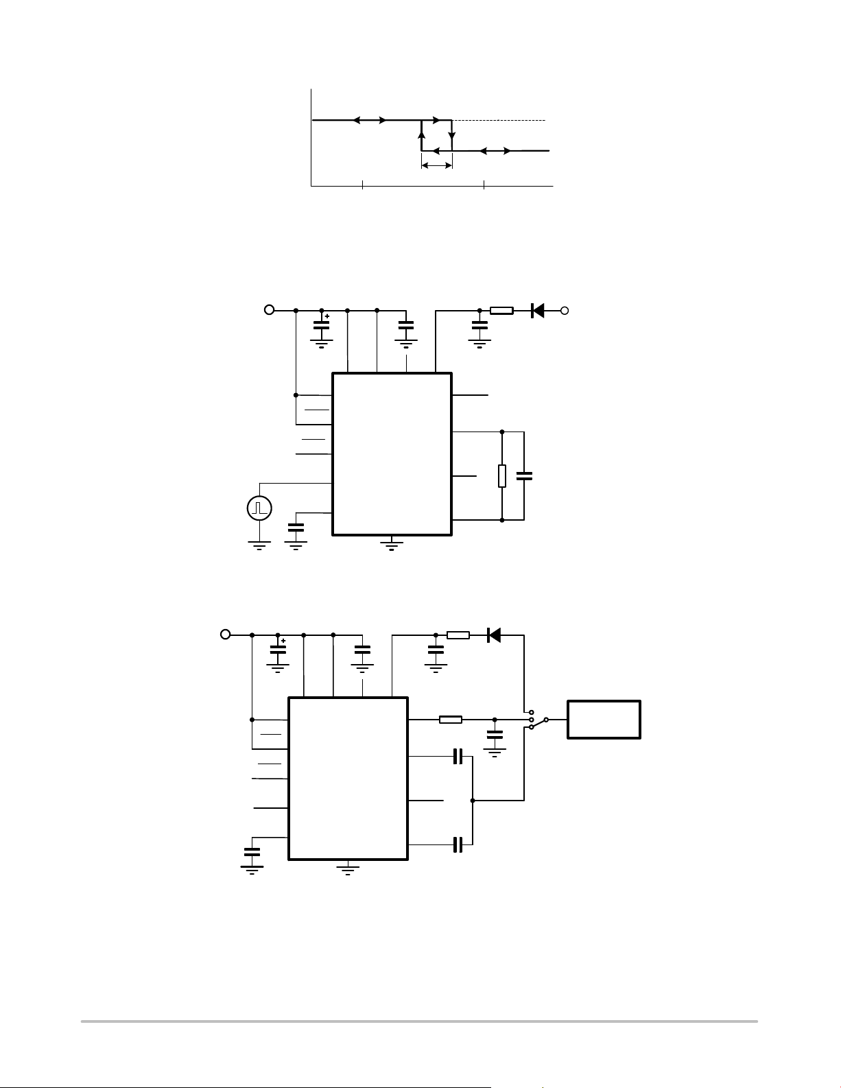
Figure 7. Hysteresis of the Receiver
0.9
V
i(dif)(hys)
High
Low
+5V
15 pF
+5V
Generator
47 mF
EN
STB
ERR
TxD
RxD
47 mF
100 nF
1kW
10 nF
EN
STB
ERR
TxD
RxD
Vio
15 pF
5
6
14
8
1
4
Vcc
37
2
INH
NCV7341
GND
VBAT
10
13
11
12
9
WAKE
CANH
V
SPLIT
CANL
R
LT
60 W
PC20060921.6
C
LT
100 pF
Figure 8. Test Circuit for Timing Characteristics
100 nF
1kW
10 nF
Vio
5
6
14
8
1
4
Vcc
37
NCV7341
2
INH
GND
VBAT
10
13
11
12
9
WAKE
CANH
V
SPLIT
CANL
10 nF
1nF
1nF
PC20060921.5
+12V
Transient
Generator
Figure 9. Test Circuit for Automotive Transients
http://onsemi.com
16
Page 17
NCV7341
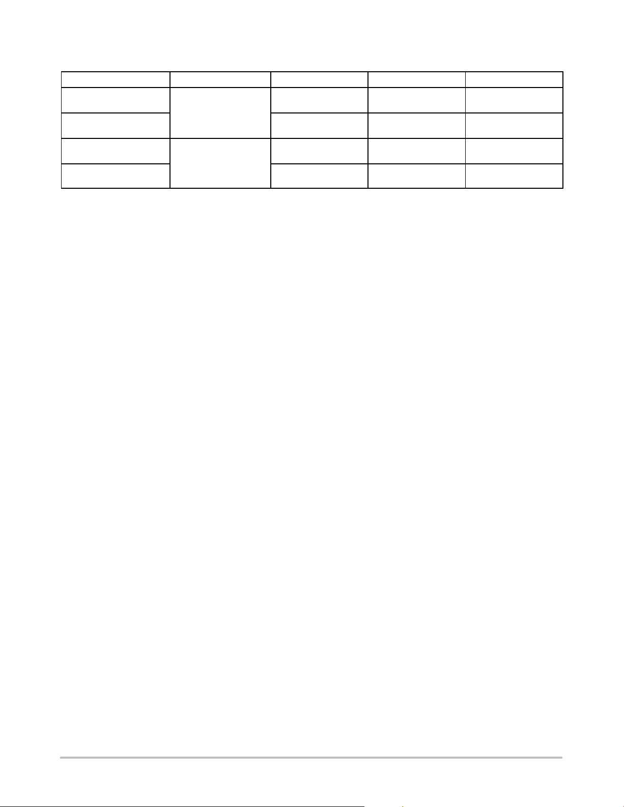
DEVICE ORDERING INFORMATION
Part Number Description Temperature Range Package Type Shipping
NCV7341D20G
NCV7341D20R2G −40°C − 125°C SOIC−14
NCV7341D21G
NCV7341D21R2G −40°C − 125°C SOIC−14
†For information on tape and reel specifications, including part orientation and tape sizes, please refer to our Tape and Reel Packaging
Specifications Brochure, BRD8011/D.
HS CAN Transceiver
with bus error detection
HS CAN Transceiver
−40°C − 125°C SOIC−14
(Pb−Free)
(Pb−Free)
−40°C − 125°C SOIC−14
(Pb−Free)
(Pb−Free)
55 Tube / Tray
3000 / Tape & Reel
55 Tube / Tray
3000 / Tape & Reel
†
http://onsemi.com
17
Page 18
NCV7341
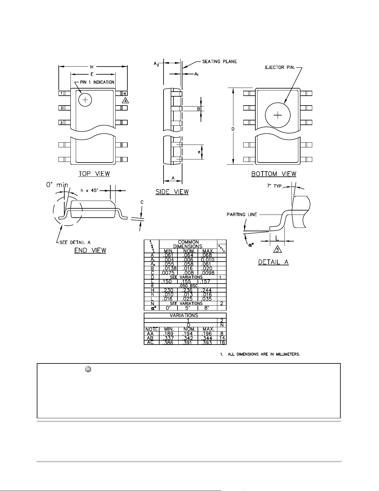
SOIC 14
CASE 751AP−01
ISSUE A
ON Semiconductor and are registered trademarks of Semiconductor Components Industries, LLC (SCILLC). SCILLC reserves the right to make changes without further notice
to any products herein. SCILLC makes no warranty, representation or guarantee regarding the suitability of its products for any particular purpose, nor does SCILLC assume any liability
arising out of the application or use of any product or circuit, and specifically disclaims any and all liability, including without limitation special, consequential or incidental damages.
“Typical” parameters which may be provided in SCILLC data sheets and/or specifications can and do vary in different applications and actual performance may vary over time. All
operating parameters, including “Typicals” must be validated for each customer application by customer’s technical experts. SCILLC does not convey any license under its patent rights
nor the rights of others. SCILLC products are not designed, intended, or authorized for use as components in systems intended for surgical implant into the body, or other applications
intended to support or sustain life, or for any other application in which the failure of the SCILLC product could create a situation where personal injury or death may occur. Should
Buyer purchase or use SCILLC products for any such unintended or unauthorized application, Buyer shall indemnify and hold SCILLC and its officers, employees, subsidiaries, affiliates,
and distributors harmless against all claims, costs, damages, and expenses, and reasonable attorney fees arising out of, directly or indirectly, any claim of personal injury or death
associated with such unintended or unauthorized use, even if such claim alleges that SCILLC was negligent regarding the design or manufacture of the part. SCILLC is an Equal
Opportunity/Affirmative Action Employer. This literature is subject to all applicable copyright laws and is not for resale in any manner.
PUBLICATION ORDERING INFORMATION
LITERATURE FULFILLMENT:
Literature Distribution Center for ON Semiconductor
P.O. Box 5163, Denver, Colorado 80217 USA
Phone: 303−675−2175 or 800−344−3860 Toll Free USA/Canada
Fax: 303−675−2176 or 800−344−3867 Toll Free USA/Canada
Email: [email protected]
N. American Technical Support: 800−282−9855 Toll Free
USA/Canada
Europe, Middle East and Africa Technical Support:
Phone: 421 33 790 2910
Japan Customer Focus Center
Phone: 81−3−5773−3850
http://onsemi.com
ON Semiconductor Website: www.onsemi.com
Order Literature: http://www.onsemi.com/orderlit
For additional information, please contact your local
Sales Representative
NCV7341/D
18
 Loading...