

Page 1
NCS6416
Low-Voltage,
Bus-Contr olled Video
Matrix Switch
Description
The main function of the NCS6416 is to switch 8 video input
sources to the 6 outputs. The NCS6416 operates with a low 5 V power
supply.
Each output can be switched to only one of the inputs, whereas any
single input may be connected to several outputs.
All switching possibilities are controlled through the I2C bus inputs.
Features
•20 MHz Bandwidth
•5 V Operating Voltage
•Cascadable with another NCS6416 (Internal Address can be changed
by Pin 7 Voltage)
•8 Inputs (CVBS, RGB, Chroma, ...)
•6 Outputs with 150 Output Driving Capability
•Possibility of Chroma Signal for each Input by Switching off the
Clamp with an External Resistor Bridge
•Bus Controlled
•6 dB Gain between any Input and Output
•-65 dB Crosstalk at 5 MHz
•Full ESD Protection
•These are Pb-Free Devices
http://onsemi.com
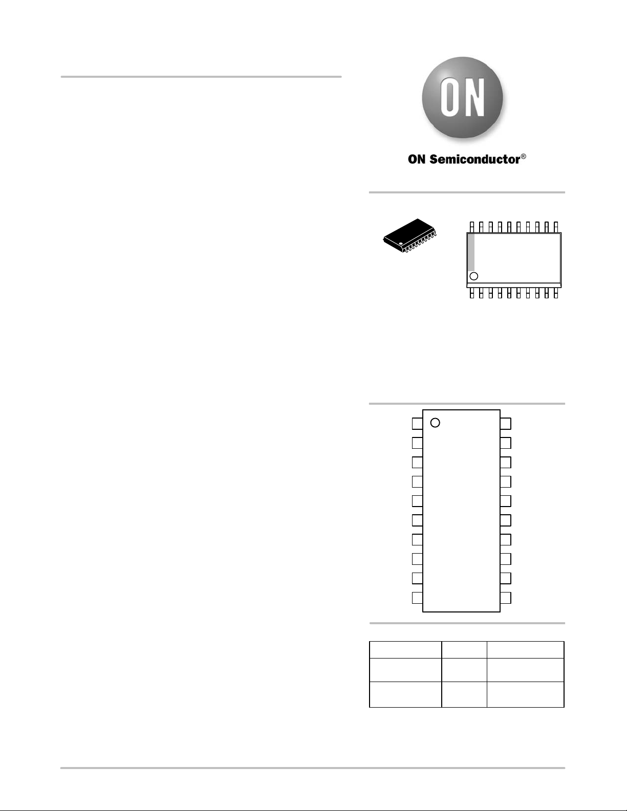
MARKING DIAGRAMS*
20
20
1
SO-20 WB
DW SUFFIX
CASE 751D
A = Assembly Location
WL = Wafer Lot
YY = Year
WW = Work Week
G = Pb-Free Package
*For additional marking information, refer to
Application Note AND8002/D.
INPUT1
DATA1
INPUT2
CLOCK
1
2
3
4
1
NCS6416
AWLYYWWG
20
19
18
17
INPUT8
V
CCO
OUTPUT6
OUTPUT5
© Semiconductor Components Industries, LLC, 2007
June, 2007 - Rev. 1
INPUT3
INPUT4
PROG
INPUT5
V
CC
INPUT6
5
6
7
8
9
10
OUTPUT4
16
OUTPUT3
15
14
OUTPUT2
13
OUTPUT1
12
GND
INPUT7
11
ORDERING INFORMATION
Device Package Shipping
NCS6416DWG SO-20
(Pb-Free)
NCS6416DWR2G SO-20
(Pb-Free)
†For information on tape and reel specifications,
including part orientation and tape sizes, please
refer to our Tape and Reel Packaging Specifications
Brochure, BRD8011/D.
1 Publication Order Number:
38 Units / Rail
1000 / Tape & Reel
†
NCS6416/D
Page 2
NCS6416
INPUT1
INPUT2
INPUT3
INPUT4
INPUT5
INPUT6
INPUT7
INPUT8
1
3
5
6
8
10
11
20
OUTPUT6
OUTPUT5
18 17 16 15 14 13 12
OUTPUT4
OUTPUT3
OUTPUT2
OUTPUT1
GND
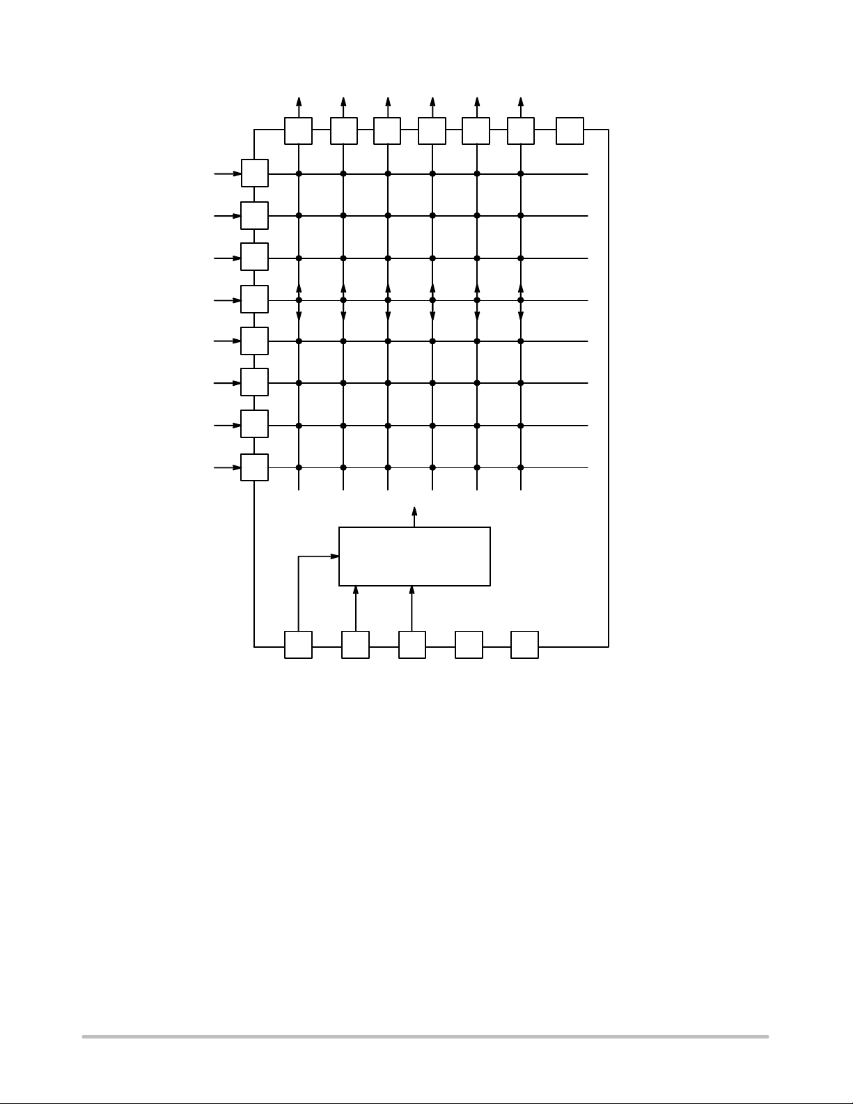
Bus Decoder
274919
CLOCKPROGDATA
Figure 1. Block Diagram
The main function of the NCS6416 is to switch 8 video
input sources to the 6 outputs.
Each output can be switched to only one of the inputs,
whereas any single input may be connected to several
outputs. The lowest level of each signal is aligned on each
input (bottom of sync pulse for CVBS or Black Level for
RGB signals). Each output is able to drive a 150 load.
The nominal gain between any input and output is 6 dB.
For Chroma signals, the clamp is switched off by forcing an
external 2.5 V DC resistor bridge on the input. Each input
NCS6416
V
CC
V
CCO
can be used as a normal input or as a Chroma input (with
external resistor bridge). All the switching possibilities are
changed through the I2C bus.
The switches configuration is defined by words of 16 bits:
one word of 16 bits for each output channel.
So, 6 words of 16 bits are necessary to determine the
starting configuration upon power-on (power supply: 0 to
5 V). But a new configuration needs only the words of the
changed output channels.
http://onsemi.com
2
Page 3
NCS6416
Table 1. ATTRIBUTES
Characteristics Value
ESD Human Body Model
Machine Model
Moisture Sensitivity (Note 1) Level 3
Flammability Rating Oxygen Index: 28 to 34 UL 94 V-0 @ 0.125 in.
1. For additional information, see Application Note AND8003/D
Table 2. MAXIMUM RATINGS
Parameter Symbol Rating Unit
Power Supply Voltage V
Output Driver Power Supply V
Operating Temperature Range T
Storage Temperature Range T
Thermal Resistance, Junction-to-Air
SO-20
Stresses exceeding Maximum Ratings may damage the device. Maximum Ratings are stress ratings only. Functional operation above the
Recommended Operating Conditions is not implied. Extended exposure to stresses above the Recommended Operating Conditions may affect
device reliability.
CC
CCO
stg
JA
2 kV
200 V
6 V
6 V
A
0 to +70 °C
-60 to +150 °C
°C/W
30 to 35
Table 3. DC & AC Characteristics (T
= 25°C, VCC = 5 V, RL = 150 , CL = 3 pF)
A
Symbol Parameter Min Typ Max Unit
V
V
I
CC
CCO
CC
Supply Voltage 4.75 5.0 5.25 V
Output Driver Power Supply 4.75 5.0 5.25 V
Power Supply Current (No Load) 20 30 40 mA
INPUTS
Signal Amplitude (CVBS signal) (Note 2) 1.0 V
Input Current (Per Output Connected) 1 3
DC Level (Bottom of Sync Pulse) 1.25 1.35 1.45 V
DC Level Shift (0°C to 70°C) (Note 2) 5 100 mV
R
IN
C
IN
Input Resistance (Note 2) 1
Input Capacitance (Note 2) 2 pF
OUTPUTS
Dynamic Range (VIN = 1 VPP) (Note 2) 1.9 2.0 2.1 V
Output Impedance (Note 2) 1
A
V
Gain (Note 2) 5.5 6.0 6.5 dB
BW Bandwidth (Note 2)
-1 dB Attenuation
-3 dB Attenuation
7 15
20
DG Differential Gain Error (Note 2) 0.5 %
DP Differential Phase Error (Note 2) 1.5 °
Crosstalk (f = 5 MHz) (Note 2) -65 -60 dB
DC Level (Bottom of Sync Pulse) 0.2 0.3 0.4 V
Continuous Output Current (Note 2) 20 mA
I2C BUS INPUT: DATA, CLOCK AND PROG
Threshold Voltage (Note 2) 1.5 2 3 V
2. Guaranteed by design and/or characterization.
PP
A
M
PP
MHz
http://onsemi.com
3
Page 4

NCS6416
Table 4. I2C BUS CHARACTERISTICS
Symbol Parameter Test Conditions Min Max Unit
SCL
V
IL
V
IH
I
LI
f
SCL
t
R
t
F
C
I
SDA
V
IL
V
IH
I
LI
C
I
t
R
t
F
V
OL
t
F
C
L
TIMING
t
LOW
t
HIGH
t
SU,DAT
t
HD,DAT
t
SU,STO
t
BUF
t
HD,STA
t
SU,STA
3. Guaranteed by design and/or characterization.
4. Functionality guaranteed by design and/or characterization.
Low Level Input Voltage -0.3 +1.5 V
High Level Input Voltage 3.0 VCC +0.5 V
Input Leakage Current VI = 0 to V
CC
-10 +10
Clock Frequency (Note 3) 0 100 kHz
Input Risetime (Note 3) 1.5 V to 3 V 1000 ns
Input Falltime (Note 3) 3 V to 1.5 V 300 ns
Input Capacitance (Note 3) 10 pF
Low Level Input Voltage -0.3 +1.5 V
High Level Input Voltage 3.0 VCC +0.5 V
Input Leakage Current VI = 0 to V
CC
-10 +10
Input Capacitance (Note 3) 10 pF
Input Risetime (Note 3) 1.5 V to 3 V 1000 ns
Input Falltime (Note 3) 3 V to 1.5 V 300 ns
Low Level Output Voltage IOL = 3 mA 0.4 V
Output Falltime (Note 3) 3V to 1.5 V 250 ns
Load Capacitance (Note 3) 400 pF
Clock Low Period (Note 4) 4.7
Clock High Period (Note 4) 4.0
Data Setup Time (Note 4) 250 ns
Data Hold Time (Note 4) 0 340 ns
Setup Time from Clock High to Stop (Note 4) 4.0
Start Setup Time following a Stop (Note 4) 4.7
Start Hold Time (Note 4) 4.0
Start Setup Time following Clock Low to High Transition
4.7
(Note 4)
A
A
s
s
s
s
s
s
http://onsemi.com
4
Page 5

NCS6416
Bus Selections
The I2C chip address is defined by the first byte. The second byte defines the input/output configuration.
Table 5. CHIP ADDRESS BYTE (1ST BYTE OF TRANSMISSION)
HEX BINARY Comment
86 1000 0110 When PROG pin is connected to Ground
06 0000 0110 When PROG pin is connected to V
NOTE: Input/Output Selection Byte (2nd byte of transmission)
Table 6. I2C BUS OUTPUT SELECTIONS
Output Address (MSB) Input Address (LSB) Selected Output
00000 XXX Pin 18 Output is selected by the 5 MSBs
00100 XXX Pin 14
00010 XXX Pin 16
00110 - Not Used
00001 XXX Pin 17
00101 XXX Pin 13
00011 XXX Pin 15
00111 - Not Used
CC
Table 7. I2C BUS INPUT SELECTIONS
Output Address (MSB) Input Address (LSB) Selected Input
00XXX 000 Pin 5 Input is selected by the 3 LSBs
00XXX 100 Pin 8
00XXX 010 Pin 3
00XXX 11 0 Pin 20
00XXX 001 Pin 6
00XXX 101 Pin 10
00XXX 011 Pin 1
00XXX 111 Pin 11
Example: 0010 0101 (Binary) or 25 (Hex) connects Pin 10 (input) to Pin 14 (output)
SDA
SCL
SDA
t
BUF
t
LOW
t
t
HD.STA
R
t
SU.STA
Figure 2. I2C Bus Timing Diagram
t
HD.DAT
t
HIGH
t
F
t
SU.DAT
t
SU.STO
http://onsemi.com
5
Page 6

Pins 1, 3,
5, 6, 8, 10,
11 and 20
Video Inputs
ESD Protection
NCS6416
V
+
DC
CCO
75 Z = 75
-
Video
Output
Input Clamp
To Switch
Matrix
Input Buffer
Video
Inputs
75
+
-
NCS6416
Figure 3. Input Configuration Figure 4. Output Configuration
Pins 2, 4, 7
I2C Bus Inputs
Input Buffer
I2C Decode Logic
75
ESD Protection
ACK
*For Pin 2
(SDA)
Figure 5. Bus I/O Configuration
USING A SECOND NCS6416
The programming input pin (PROG) allows two NCS6416 circuits to operate in parallel and to select them independently
through the I2C bus by modifying the address byte. Consequently, the switching capabilities are doubled, or can be cascaded
as shown in Figure 6.
NCS6416
SDA/SCL
MCU
Logical “0”
Video Inputs
Logical “1”
PROG
Video Outputs
NCS6416
SDA/SCL
PROG
Video Inputs
Figure 6. Cascaded NCS6416
http://onsemi.com
6
Video Outputs
Page 7

NCS6416
TYPICAL APPLICATION DIAGRAM
NCS6416 is suited for single supply system, running on
a single +5 V supply. It can drive a 150 video output due
to the built-in low impedance and high current video output
stage. The high quality of the output stage and excellent
Additional Video Inputs
17 15
18
Security
Video
Interface
Satellite TV
receiver
circuit
1
3
5
6
8
10
11
20
Output 6
Input 1
Input 8
SDA
Prog
linearity provides video signal comparable to broadcast
studio quality signals. The layout is not as critical to the
design and it can be easily realized on a single sided board.
Bus
14
13
Screen
Outpu 1
VCR
Additional Video Outputs
NCS6416
16
Decoder
SCL
HDTV
Receiver
circuit
V
CCO
Microcontroller
Figure 7. Typical Application Diagram
http://onsemi.com
7
Page 8

NCS6416
100F
C10 C11
V
CCO
10F
= +5V
Input 1
SDA
Input 2
SCL
Input 3
Input 4
VCC = +5V
Input 5
Input 6
VCC = +5V
R7
75
R1
75
R3
75
R5
75
R6
75
R8
75
H
F
C9
C1
100
C2
R4
C3 100nF
C4 100nF
C6 100nF
C7
100nF
V
CCO
GND
20
19
18
17
16
15
14
13
12
11
100nF
R2
100nF
100
C8
100nF
1
INPUT1
2
DATA
3
INPUT2
4
CLOCK
5
INPUT3
6
INPUT4
7
PROG
8
INPUT5
9
V
CC
10
INPUT6
INPUT8
OUTPUT6
OUTPUT5
OUTPUT4
OUTPUT3
OUTPUT2
OUTPUT1
INPUT7
Figure 8. Typical Application Circuit
C12 100nF
R10
75
R11
75
R12
75
R13
75
R14
75
R15
75
C13 100nF
R9
75
R11
75
Z = 75
Z = 75
Z = 75
Z = 75
Z = 75
Z = 75
Input 7
Input 8
75
75
75
75
75
75
Output 6
Output 5
Output 4
Output 3
Output 2
Output 1
http://onsemi.com
8
Page 9

NCS6416
PACKAGE DIMENSIONS
SO-20 WB
CASE 751D-05
ISSUE G
H10X
M
B
M
0.25
D
20
1
B20X
M
SAS
T
18X
0.25
e
A
11
_
E
10
h X 45
B
B
A
SEATING
PLANE
A1
T
q
NOTES:
1. DIMENSIONS ARE IN MILLIMETERS.
2. INTERPRET DIMENSIONS AND TOLERANCES
PER ASME Y14.5M, 1994.
3. DIMENSIONS D AND E DO NOT INCLUDE MOLD
PROTRUSION.
4. MAXIMUM MOLD PROTRUSION 0.15 PER SIDE.
5. DIMENSION B DOES NOT INCLUDE DAMBAR
PROTRUSION. ALLOWABLE PROTRUSION
SHALL BE 0.13 TOTAL IN EXCESS OF B
DIMENSION AT MAXIMUM MATERIAL
CONDITION.
MILLIMETERS
DIM MIN MAX
A 2.35 2.65
A1 0.10 0.25
B 0.35 0.49
C 0.23 0.32
D 12.65 12.95
E 7.40 7.60
e 1.27 BSC
L
C
H 10.05 10.55
h 0.25 0.75
L 0.50 0.90
q 0 7
__
ON Semiconductor and are registered trademarks of Semiconductor Components Industries, LLC (SCILLC). SCILLC reserves the right to make changes without further notice
to any products herein. SCILLC makes no warranty, representation or guarantee regarding the suitability of its products for any particular purpose, nor does SCILLC assume any liability
arising out of the application or use of any product or circuit, and specifically disclaims any and all liability, including without limitation special, consequential or incidental damages.
“Typical” parameters which may be provided in SCILLC data sheets and/or specifications can and do vary in different applications and actual performance may vary over time. All
operating parameters, including “Typicals” must be validated for each customer application by customer's technical experts. SCILLC does not convey any license under its patent rights
nor the rights of others. SCILLC products are not designed, intended, or authorized for use as components in systems intended for surgical implant into the body, or other applications
intended to support or sustain life, or for any other application in which the failure of the SCILLC product could create a situation where personal injury or death may occur. Should Buyer
purchase or use SCILLC products for any such unintended or unauthorized application, Buyer shall indemnify and hold SCILLC and its officers, employees, subsidiaries, affiliates,
and distributors harmless against all claims, costs, damages, and expenses, and reasonable attorney fees arising out of, directly or indirectly, any claim of personal injury or death
associated with such unintended or unauthorized use, even if such claim alleges that SCILLC was negligent regarding the design or manufacture of the part. SCILLC is an Equal
Opportunity/Affirmative Action Employer. This literature is subject to all applicable copyright laws and is not for resale in any manner.
PUBLICATION ORDERING INFORMATION
LITERATURE FULFILLMENT:
Literature Distribution Center for ON Semiconductor
P.O. Box 5163, Denver, Colorado 80217 USA
Phone: 303-675-2175 or 800-344-3860 Toll Free USA/Canada
Fax: 303-675-2176 or 800-344-3867 Toll Free USA/Canada
Email: orderlit@onsemi.com
N. American Technical Support: 800-282-9855 Toll Free
USA/Canada
Europe, Middle East and Africa Technical Support:
Phone: 421 33 790 2910
Japan Customer Focus Center
Phone: 81-3-5773-3850
http://onsemi.com
ON Semiconductor Website: www.onsemi.com
Order Literature: http://www.onsemi.com/orderlit
For additional information, please contact your local
Sales Representative
NCS6416/D
9
 Loading...